T
T
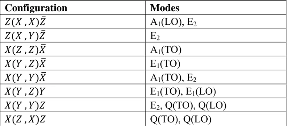
H
H
È
È
S
S
E
E
En vue de l'obtention du
D
D
O
O
C
C
T
T
O
O
R
R
A
A
T
T
D
D
E
E
L
L
’
’
U
U
N
N
I
I
V
V
E
E
R
R
S
S
I
I
T
T
É
É
D
D
E
E
T
T
O
O
U
U
L
L
O
O
U
U
S
S
E
E
Délivré par l'Université Toulouse III - Paul SabatierDiscipline ou spécialité : Physique de la matière
JURY B. JUSSERAND Rapporteur O. PAGES Rapporteur B. DAUDIN Examinateur F. MORANCHO Examinateur L. DURAND Examinateur A. MLAYAH Examinateur R. PECHOU Examinateur
Ecole doctorale : Ecole Doctorale Sciences de la Matière
Unité de recherche : Centre d’Elaboration de Matériaux et d’Etudes Structurales Directeur(s) de Thèse : F. DEMANGEOT
Présentée et soutenue par Jiangfeng WANG Le 18/10/2013
Titre : Vibrations optiques dans les nanofils polaires de Nitrure de Gallium: une étude des effets de la dimension, du rapport d'aspect et de la densité
Optical vibrations in polar GaN nanowires: a study of size, aspect ratio and density effects
1
Abstract
This thesis presents mainly a detailed investigation of the optical properties of GaN nanowires (NWs) ensemble and single GaN NW in particular by Raman spectroscopy. The Raman scattering in GaN/AlN superlattice has also investigated. NWs are often considered as potential building blocks for future nanometer scaled devices. This is based on several attractive features that are generally ascribed to NWs. For instance, they are expected to grow strain free and defects even on substrates with a large structural mismatch. This can be examined in different NWs samples by the Raman frequency and line width of non-polar E2h phonon.
In the first part of the thesis, the characterization of morphologies, structure, dimensions and orientation have been investigated in the GaN NWs grown on Si substrates by plasma assisted molecular beam epitaxy (PA-MBE) without any catalyst. These results indicate good crystallization quality of MBE and several inhomogeneity of NWs.
The major part of this thesis discusses the vibrational properties of GaN NWs. The investigation of Raman scattering of NWs ensemble and single NW reveal the significant phonon behavior as a function of their large surface-to-volume ratio. First, certain optical features are only found in the Raman spectra of GaN NWs but not in that of bulk GaN. An unexpected emergence of a two peaks band located near 700 cm-1 has been found in the undoped NWs but not in Si-doped NWs. This is attributed to the Raman scattering by surface related modes and has been confirmed by their high sensitivity to the dielectric constant of the NWs surrounding medium. We used an effective dielectric continuum model to interpret and detailed analyze these observations. Second, the optical characteristics of individual NW are also investigated in this context. The dependence of Raman intensity on the size of NWs and polarization of light excitation has been studied. The observed enhancement of A1(TO) mode and a shoulder in high frequency side are strongly related to excitation
wavelength and the aspect ratio of single NW. The frequencies and distribution of light electric field inside NW of these modes have been analyzed by a DDA-based calculation model.
The Raman scattering of core-shell structural NWs and GaN/AlN superlattice are also discussed. By using UV resonant excitation, double strain states induced by AlN shell have been found in GaN/AlN core-shell structural NWs and the interface mode has been observed in addition to the Quasi-Longitudinal Optical mode in the GaN/AlN superlattice. Finally,the analysis of stress distribution on crack free thick GaN layers has been performed by Raman measurement. We have investigated the influence of different sizes and trench height of GaN mesa on the strain distribution. This strain/stress field was modeled within the framework of linear elasticity theory using finite element method (FEM).
Keyword:
3
Résumé
La thèse présente une analyse détaillée des propriétés optiques d’assemblées de nanofils de GaN mais aussi de nanofils individuels, menée essentiellement par diffusion inélastique de la lumière par les excitations du réseau cristallin. Des études ont été également menées dans des nanofils contenant des super-réseaux GaN/AlN. Ces nano-objets pourraient jouer un rôle clef dans les dispositifs à l’échelle nanométrique de demain, en raison notamment de leur très grande qualité structurale et de leur faible niveau de déformation interne, confirmés par l’analyse de la raie Raman correspondant au mode de vibration optique non polaire de symétrie E2 de
haute fréquence.
Dans la première partie de la thèse, une étude des différents paramètres est proposée dans des nanofils GaN fabriqués par épitaxie par jets moléculaires assistée Plasma sur substrat Silicium : morphologie, structure cristalline, dimension et orientation. Les résultats démontrent une certaine inhomogénéité des nanofils sur leur substrat.
La partie centrale de la thèse se focalise sur les propriétés vibrationnelles des nanofils de GaN.
D’une part, les spectres Raman révèlent un comportement caractéristique du grand rapport surface/volume associé à ces nano-objets, qui les différencient nettement du comportement du matériau massif. En particulier, la thèse fournit une analyse détaillée de nouvelles signatures spectrales dans la partie haute fréquence des spectres, en fonction de différents paramètres expérimentaux liés au matériau et aux mesures Raman: dopage, orientation, densité, environnement diélectrique extérieur, paramètres d’illumination de la surface. Nous avons pu ainsi démontrer qu’il s’agit de vibrations localisées à la surface des nanofils, et dont nous proposons une description simple en un milieu moyen décrit par une fonction diélectrique effective.
D’autre part, une étude Raman systématique est aussi proposée en fonction de la polarisation du laser excitateur, de la dimension et du rapport d’aspect de nanofils GaN analysés individuellement. L’exaltation de l’intensité de la diffusion Raman par le mode transverse optique de symétrie A1(TO) et d’un épaulement associé, est
corrélée à la longueur d’onde d’excitation et au rapport d’aspect des nanofils. Le bon accord observé avec les résultats de calculs réalisés dans le cadre de l’approximation par dipôles discrets (DDA) indique que ces deux signatures sont associées à des vibrations confinées dans le nanofil. Ces calculs indiquent en outre, que les vibrations localisées aux surfaces sont insensibles au rapport d’aspect du nanofil, en bon accord avec les résultats expérimentaux.
L’étude de nanofils individuels GaN fonctionnalisés par insertion de disques quantiques AlN est aussi présentée. L’utilisation de la diffusion Raman résonnante permet d’augmenter la sensibilité de la sonde vibrationnelle et de mettre en évidence des fluctuations structurales à l’intérieur d’un nanofil unique. Enfin, nous proposons l’analyse de la distribution des déformations dans des couches épaisses de GaN épitaxiées sur des mesas sur substrat Silicium. Une analyse systématique de
l’influence de la dimension et de la hauteur de tranchées associées aux mesas GaN sur la distribution des déformations est conduite en couplant étroitement cartographie Raman et calculs dans le cadre de la théorie de l’élasticité linéaire utilisant la méthode des éléments finis.
Mots Clefs :
5
Acknowledgements
Firstly I am really grateful to my thesis director François DEMANGEOT and Renaud PECHOU for their full support, guidance, encouragement and sincerity which help me all the way to complete my Ph.D. work. Both François DEMANGEOT and Renaud PECHOU guided me in understanding the GaN NWs properties and Raman analysis. I always enjoyed their suggestions and advices which helped me to understand and resolve the challenges in my research work, especially their scrupulous attitude and spirit to the research.
I would like to acknowledge Lise DURAND and Anne PONCHET, who help me in the simulation and calculation of the elastic strain with their patience. I would also like to acknowledge Prof. Adnen Mlayah who helps me to understand the electron-phonon interaction in single NWs with the DDA simulation.
I am thankful to Bruno DAUDIN from CEA/CNRS group (Nanophysique et Semiconducteurs, CEA Grenoble) for providing the high qualities nanowires samples and information about their synthesis, PL analysis.
Many thanks to Antoine Zwick , Frédéric Neumayer and Sebastien Moyano for providing technical support for Raman experiments in CEMES. Thanks to Christophe Deshayes for the SEM training and supports on the NWs morphological analysis.
My sincere thanks go to the director of CEMES Jean-Pierre Launay, and all the members of his secretariat, for providing me the chance to join the CEMES for my PhD and helping me in administrative procedures to complete my thesis.
Finally, I take this opportunity to thank my parents and my wife, for their love and support.
7
Contents
Abstract ... 1 Résumé ... 3 Acknowledgements ... 5 Contents ... 7 Chapter 1 Introduction ... 9 1.1 Objective of this thesis ... 9 1.2 Overview of III Nitride semiconductor material and applications ... 10 1.3 Choice of the substrates for GaN epitaxy ... 11 1.4 The growth technologies of GaN nanowires ... 13 1.5. Techniques for the material characterization ... 14 1.5.1 Scanning Electron Microscopy (SEM) ... 15 1.5.2 Atomic Force Microscopy (AFM) ... 16 1.5.3 Focused ion beam (FIB) ... 17 1.5.4 Raman scattering ... 19 1.6 Overview ... 25 References ... 27 Chapter 2 Structure and Properties of III nitrides ... 31 2.1 Introduction ... 31 2.2 Crystal Structure of Nitrides ... 32 2.3 Vibration properties ... 33 2.3.1 Crystal symmetry properties ... 33 2.3.2 Phonon dispersion and energy band ... 34 2.3.3 Raman tensors and selection rules ... 38 References ... 43 Chapter 3 Raman studies of GaN nanowires ensemble ... 45 3.1 GaN NWs Sample growth and experimental preparation ... 45 3.2 Visible Raman scattering in GaN NWs ... 48 3.2.1 Surface optical phonon scattering ... 51 3.2.2. Dielectric continuum theoretical simulation for surface optical modes ... 60 3.3 Photoluminescence in GaN nanowires ... 69 3.4 Ultraviolet Raman scattering in GaN nanowires ... 72 3.5 Conclusion ... 74 References ... 77 Chapter 4 Vibrational analysis of single NWs ... 81 4.1 Sample preparation and experimental approach ... 82 4.2 Visible Raman scattering in single GaN NWs ... 85 4.2.1 Raman measurements on single GaN NWs ... 85 4.2.2 Theoretical simulation of size and aspect ratio effects ... 91 4.3 UV Raman scattering in a single GaN and GaN/AlN NWs ... 96 4.4 Conclusion ... 99 References ... 101Chapter 5 Study of strain in GaN epitaxy grown on silicon by Raman spectroscopy and finite element method ... 103 5.1 Introduction ... 103 5.2 Raman characterization of GaN layer ... 103 5.2.1 Description of sample ... 103 5.2.2 Strain effect on phonon modes ... 104 5.2.3 Raman measurements and results ... 106 5.3 Finite element method (FEM) modeling ... 110 5.3.1 Modeling principle ... 113 5.3.2 Simulation Results and discussion... 117 5.4 Conclusion ... 121 References ... 123 Chapter 6 Conclusion ... 125
9
Chapter 1 Introduction
1.1 Objective of this thesis
The material system of interest in this thesis is the wide band gap III-nitride semiconductor gallium nitride (GaN) nanowires (NWs) and GaN/AlN superlattice NWs. III-Nitrides have attracted lots of attention as promising materials for optoelectronic applications from blue to ultraviolet range. NWs are often considered as potential building blocks for future nanometer-scaled devices. Due to the lack of lattice matched substrates, there are high defects density and strain induced by thermal expansion coefficient mismatch and lattice mismatch in the traditional 2D GaN-based devices, which limit the devices performance. However, the interface dimension in NWs is considerably reduced. As a consequence, extended defects are bound to bent to the nearby surface rather than propagating along the entire crystal. Furthermore, an efficient elastic strain relaxation is expected at the interface of the NWs and the substrate [1-3]. In other words, NWs are believed to be essentially free of strain and extended defects, and their functionality is independent of the chosen substrate. It also allows the compatibility and availability of current semiconductor manufacturing technologies and the large size (up to 12 inch in silicon substrate) with low cost. Meanwhile, the absence of defects in the superlattice NWs structures may drastically improve the performance of optical devices such as light emitting diodes (LEDs) [4]. Due to 1D geometry of NWs, the efficient coupling of light is also expected for photodetectors, solar cells and LEDs. The applications based on GaN NWs have also been reported such as field effect transistors [5], photodetectors [6], sensors [7] and lasers diode [8].
The optical and vibrational properties of GaN NWs are strongly different compared to conventional macroscopic material. There are still many aspects of fundamental optical and electrical properties poorly understood by their strongly anisotropic geometry. In this context, the purpose of this thesis is to understand vibrational and optical properties in GaN NWs which were grown by plasma-assisted Molecular Beam Epitaxy (MBE). My work focuses on the optical properties of both GaN NWs ensemble and single GaN NWs. We combine Raman spectroscopy, atomic force microscopy (AFM) and scanning electron microscopy (SEM) to analyze these NWs. We characterize these properties of pure GaN nanowires (non functional) and GaN/AlN heterostructure nanowires (functional) from ensemble to single, attempting to explain the observations that we measured in the Raman experiments. Particular attention has been paid to surface-related effects due to their large surface-to-volume ratio, which can possibly influence the electrical properties of devices. We also investigate vibration properties of the GaN/AlN superlattice NWs and core/shell structure NWs. Finally, we study the strain distribution in GaN epilayer grown on silicon (110) substrate as a function of mesa size, thickness, silicon pattern height. These samples are grown by metal organic chemical vapor deposition (MOCVD).
1.2 Overview of III Nitride semiconductor material and
applications
Following the first generation (Si, Ge) and the second generation (GaAs, InP), the III-nitride known as the third generation semiconductor materials, have attracted extreme attention either in the laboratory investigations or in the commercial area. III-nitride GaN, AlN, InN can form alloys, whose band gap can cover a continuum range from the red 1.9eV (653nm) to ultraviolet 6.2eV (200nm). GaN as a kind of promising semiconductor material has favorable material properties, such as high electron mobility and high electron saturated velocity. In recent years, more and more efforts have been made to realize its promising applications in shortwave light emitting devices, photo-detectors, high power and high frequency electronic devices.
GaN is a very hard, mechanically stable material. GaN (3.42eV) and SiC (3.26eV) have large bandgap energies about two or three time of those in conventional semiconductor such as Si (1.12eV), GaAs (1.43eV) and InP (1.35eV). The high electric breakdown fields in GaN due to the large bandgap allow the application of high power, high temperature area. Moreover, the thermal conductivity of a semiconductor material is very important. Poor thermal conductivity leads to degraded device operation at elevated temperature. Conventional semiconductors are poor thermal conductors, particularly GaAs and InP. Conversely, SiC is excellent thermal conductor and GaN is comparable with Si. Due to the lack and immaturity of heterojunction technology for SiC, it does not challenge the GaN-based material.
GaN was synthesized firstly by Juza and Hahn in the 1938s [9].The significant breakthrough had been made in 1971 by Pankove et al.[10]. They achieved the first GaN light emitting diode (LED) with Zn-doped p-type layer although the luminescent efficiency was very low. But little progress has been made after that in controlling the high intrinsic n-type conductivity and obtaining conducting p-type GaN films. Until 1991, Nakamura developed the first Mg-doped homojunction blue LEDs on sapphire substrate. They have increased the brightness to 1cd from InGaN/AlGaN heterostructures[11] in 1993 and reached 2cd in 1995. With the improvement of the crystalline quality and some processing such as of Al2O3 passivation layers
disposition on the surface [12], the brightness can be improved about 13.6% higher than the conventional LEDs. High brightness blue LEDs have been hugely used in the commercial field for full color displays, high density optical information storage, etc. Today, the brightness of LED lamp based on GaN-on-GaN can achieve center-beam candle power (CBCP) of 2375 cd at 25° beam angle.[13]
For the laser (LD) applications, the current DVD systems use a red LD with wavelength of 650nm. GaN-based blue-violet LDs with an emission wavelength of 405nm will be applied for next generation DVD and optical high density data storage systems. Using these blue-violet LDs it is already possible to write huge amounts of data (27GB) on a single-layer DVD disk. At present, Tokyo Sony Company has led a so-called blue ray Disc, which is pushing one of two competing standards for the
11 design of the disc, players and recorders that use blue GaN based LDs. Other GaN based LD applications are laser printing, projection displayers, and medical, etc. In spite of the rapid development of the III-nitrides materials, their growth of high quality with low cost are still difficult to achieve. No suitable substrate material with a reasonably close lattice match is the main problem. Although sapphire has been industrial choice of GaN based epitaxy as a substrate, it has many difficulties in making large diameter wafers caused by material hardness. In the point of large diameter GaN based epitaxy for LED and power device applications, silicon is the most promising substrate of GaN epitaxy if one can eliminate cracks and improve the crystal qualities because it has been already ready for up to 12 inch with low cost. The choice of the substrate for GaN epitaxy will be discussed below.
1.3 Choice of the substrates for GaN epitaxy
The most challenging aspects of GaN based devices come from the lack of a suitable substrate. The excellent performance GaN based devices could be reached by the use of homoepitaxy on bulk GaN substrates. However three-dimensional crystals of GaN are not produced on a commercial scale. We rely only on heteroepitaxy in preparation of devices based on GaN. In practice for heteroepitaxy, not only lattice constants and thermal properties are of a great importance, but also the structure of crystal material, treatment of a surface, chemical and electric properties of the material used, have also a great influence on selection of the substrates. The most common substrate materials used today have very different properties than the GaN layer itself. We consider mostly the following factors for a suitable substrate.
(1) the less lattice mismatch as possible.
(2) closer thermal expansion coefficient as possible. (3) the wafer size, price, etc.
- Sapphire (Al
2O
3):
Traditionally, Sapphire is the most commonly used substrate for GaN Epitaxy. It is an interesting choice because it is semi-insulating. It can withstand the required high growth temperature and it is relatively cheap ($100/2 inch). The growth technology is relatively mature and it does not absorb visible light. Meanwhile, the large lattice mismatch with GaN has been reduced by deposition of buffer layers
[14-16]. However, the thermal expansion coefficient of sapphire is higher than that of GaN, and therefore biaxial compressive strain arises in an epitaxial layer during cooling process. It is difficult for cleavage due to its poor mechanical property. The poor thermal conductivity of the device is not in evidence under a small current but it degenerates with great current in power devices.
- Silicon carbide (SiC):
Silicon carbide (SiC) has a number of advantages over sapphire for GaN growing. First of all, the lattice mismatch with GaN is low (3.1%). In addition, the thermal
conductivity coefficient of SiC is high (3.8 Wt/cmK at 300K), whereas, doped SiC possesses high electrical conductivity. It implies that electric contacts can be made on the reverse side of a substrate, and the technology of device manufacturing is relatively simplified. The cleavage is convenient and it has a good chemical stability, electrical and thermal conductivity. But the crystal quality has less performance than Sapphire and Si. The main limitation of silicon carbide lies in its high cost. A high-quality 4 inch wafer costs about 3000 $ and wafer of a larger diameter are not available. In addition, at the end of growth process, we need to etch off an initial substrate. This is a hard task in the case of SiC, because etching off SiC is a very tedious and complex process. The significant issue for SiC substrate so far is to reduce the costs and improve the crystal quality.
- Aluminium nitride (AlN):
Single-crystal aluminum nitride (AlN) substrates are possibly the best candidates for the heteroepitaxial growth of GaN epilayers because they have the same structure (wurtzite), high thermal conductivity (2.85 – 3.2 W/cmK at 300 K), high electrical resistivity (107 – 1013 Wcm) [17], and their lattice mismatch (2.4 %) and thermal
expansion coefficient mismatch (approximately 5.2 % from RT up to 1000°C) are very low. As a result of the last two properties, the defect density of GaN epitaxial layers on AlN substrates is on the order of 103 - 104 cm−2 for 2 inch substrates [18], which is about four to five orders of magnitude lower than that of layers grown on 2 inch SiC substrates. However it should be noted that the growth of high-quality large diameter bulk AlN substrates has proven to be very complicated. Only since early 2006, the US-based company Crystal IS has made 2 inch single-crystal AlN substrates available for the first time [18]. First AlGaN/GaN HFETs fabricated on small AlN substrates have shown DC current-voltage characteristics comparable to those fabricated on SiC [19].
- Silicon (Si):
Although sapphire has been industrial choice of GaN based epitaxy as a substrate, it has many difficulties in making large diameter wafers. In the point of large diameter GaN based epitaxy for LED and power device applications, silicon (Si) is the most promising substrate of GaN epitaxy if we can eliminate cracks and improve the crystal qualities.
Si wafer as a substrate of GaN has many advantages, such as excellent physical properties, a high crystal quality, low cost of epitaxial growth, good electrical conductivity, thermal conductivity and stability. In addition, the possibility to integrate optoelectronic devices on GaN-base with Si-microelectronics appears to be very attractive. However, the great lattice (17%) and thermal mismatch (56%), the facility to form amorphous silicon nitride (SiN) have restricted the GaN based devices development. It is difficult to obtain a perfect GaN layer on Si without crack.
Both cubic and hexagonal GaN can be grown on Si (001) and sometimes buffer Al2O3, AlN, AlxGa1-xN layers are used. However, the epitaxial layer prepared within
13 preferable to grow GaN. The best buffer layers to avoid the formation of an amorphous SiN and improve crystalline quality SiC and AlN.
1.4 The growth technologies of GaN nanowires
Strong interest has been devoted to the research in solid state physics of these nanostructured materials, thanks to the latest developments in preparation methods like MOVPE ( Metal Organic Vapor Phase Epitaxy ), MBE (molecular beam epitaxy) and lithography etc. These techniques allow to prepare nano-sized semiconductors with excellent crystalline quality and most often also with epitaxially determined orientations with respect to a template. The GaN nanowires can be grown with or without catalysts. We introduce two main technologies, which will be described below: the Molecular Beam Epitaxy (MBE) and the Metal-Organic Chemical Vapour Deposition (MOCVD).
- Molecular Beam Epitaxy (MBE):
MBE is one of several methods of depositing single crystals. It was invented in the late 1960s at Bell Telephone Laboratories by J. R. Arthur and Alfred Y. Cho [23]. It is a technique for epitaxial growth via the interaction of one or several molecular or atomic beams that occurs on a surface of a heated crystalline substrate. The solid sources materials are placed in evaporation cells to provide an angular distribution of atoms or molecules in a beam. The substrate is heated to the necessary temperature and, when needed, continuously rotated to improve the growth homogeneity. In the MBE process, the constituent elements of a semiconductor in the form of “molecular beams” are deposited onto a heated crystalline substrate. The “molecular beams” are typically from thermally evaporated elemental sources or gases. The growth rate are typically on the order of a few /s and the beams can be shuttered in a fraction of a second, allowing for nearly atomically abrupt transition from one material to another. At low deposition rates, the growth process can be thus monitored and a crystal may be built one atomic layer at a time [24]. Nitride semiconductors are usually grown with “plasma-assisted” MBE where active nitrogen (N2) is produced by a plasma
source.
Ultra high vacuum (UHV) is the essential environment for MBE. The rate of nitrogen evolution in the reaction chamber has to be controlled as low as possible. Therefore, the thickness of the epilayer can be precisely controlled. However, the growth time is too long to meet the production of thick epitaxial layer devices such as LEDs, LDs.
- Metal Organic Chemical Vapor Deposition (MOCVD)
The metal organic chemical vapor deposition (MOCVD) originated in the pioneering work of H. M. Manasevit [25]. It is also called metal organic vapor phase epitaxy (MOVPE). It has evolved as a leading technique, with the increasing innovations in nitride based optoelectronic technology is the main method of epitaxial
growth of materials, especially compound semiconductors. In the early 1980s, it was argued whether MOCVD could ever compete with MBE with respect to the quality of epitaxy such as thickness control, composition uniformity and the interface abruptness of the grown materials. MBE is problematic of growing Nitride- and Phosphide-based III-V semiconductors. While MOCVD, has been renowned for its high production capability and its large variety of source materials using metal organic compounds. Large scale manufacturing potential of MOCVD is an important attribute of this technique. Hence, today MOCVD has become as the preferred and better candidate for large scale production of GaN based commercial optoelectronic applications due to its moderate growth rate and the precise control of film thickness of process.
In the MOCVD process, gaseous precursors of the semiconductor elements are mixed with transport gases and injected into a reactor. These precursors are pyrollysed onto a heated substrate and react with the surface. The growth temperature is 550°C – 700°C due to the stable growth rates. Different with MBE, which is mostly a physical deposition in ultra-high vacuum conditions, MOCVD involves complex gas phase and surface chemical reactions [26] and is performed at higher gas pressures (typically 800 mbar for GaN). Metal organic molecules such as trimethyl-gallium or trimethyl-aluminum are used as precursors for Gallium and Aluminium, while ammonia (NH3) is used as a source for nitrogen. A typical deposition process for MOCVD growth of GaN can be expressed as:
Ga CH vapour NH vapour solid 3CH vapour This expression above is a very simplified one and ignores the specific reation path and growth process is inadequately understood so far.
Recently, it is reported that catalyst-free GaN nanowires have been grown with MOCVD on a -phase sapphire substrate covered with a thin dielectric layer [27]. It is based on a thin SiNx in situ deposited layer that must be carefully controlled to
promote the formation of the GaN seeds required for the wires growth.
1.5. Techniques for the material characterization
In this work, NWs under study were grown on Si substrate by PA-MBE. The preliminary examination of the NWs topographies, dimensions and surface quality were analyzed by scanning electron microscope (SEM) and atomic force microscopy (AFM). SEM was used for the overall 2D variation in surface structures in a large area view at once from hundreds even to several , whereas AFM was used rather for analyzing 3D nature of the surface in a maximum scanning area of 100 100 . Preparation of substrates to deposit single NW was realized by focused ion beam (FIB) which allows us to grave some marks above. Further and detailed studies related to vibrational properties of GaN have been performed by Raman spectroscopy. We will introduce these techniques as below.
15
1.5.1 Scanning Electron Microscopy (SEM)
SEM is an established technique for surface topography and chemical composition analysis in various disciplines of science and technology. The electrons interact with the sample within a few nanometers to several microns of the surface, depending on beam parameters and sample type. Electrons are emitted from the sample as either secondary electrons or backscattered electrons. The most common mode of detection is by secondary electrons in SEI mode. They are the signal used for investigations of surface morphology. They are produced as a result of interactions between the beam electrons and weakly bound electrons in the conduction band of the sample. Some energy of the beam electrons is transferred to the conduction band electrons in the sample, providing enough energy for their escape from the sample surface as secondary electrons. They are low energy electrons (<50eV), so only those located within the first few nanometers of the surface have enough energy to escape and be detected. On the other hand, high energy beam electrons which are scattered back out of the sample (backscattered electrons (BSE)) can provide information of different elements in the sample in the BSE mode. They can emerge from the sample at a much larger distance away from the impact of the incident beam which makes their spatial distribution larger. The intensity of BSE signal is stronger than that of secondary electrons. Once these electrons escape from the sample surface, they are typically detected by a photomultiplier detector.
Figure 1.1. Schematic of the components of a typical SEM
A schematic of a typical SEM is shown in Figure 1.1. An electron gun at the top produces a beam of monochromatic electrons which is condensed by the first condenser lens and limits the amount of current in the beam. It works in conjunction with the condenser aperture to eliminate the high angle electrons form the beam. The second condenser lens forms the electrons into a thin, tight, coherent beam. Then a set of deflection coils “scan” or “sweep” the beam in the grid manner, detecting points for a period of time determined by the scan speed. When the beam strikes the sample, interactions occurs at the surface and secondary electrons are emitted from the sample at each x, y data point during the rastering of the electron beam across the surface. The SEM image is formed as the result of the intensity of those secondary electrons.
Electron emission from the filament to the sample is produced by applying a voltage between the sample and filament. This occurs in a vacuum environment ranging from 10-4 to 10-10 Torr. The resolution of a SEM can be represented by wavelength of an electron which is written as
λ
V V , where m is the electron mass and c is the velocity of light.
With an applied voltage at 10 kV, the electron wavelength is 0.12 nm. This resolution is sufficient for surface investigation of our NWs samples.
1.5.2 Atomic Force Microscopy (AFM)
AFM is used for qualitative and quantitative measurement of near surface characteristics of samples with atomic resolution, such as surface quality, cracks, local variations and roughness.
AFM consists of a scanning sharp tip on the end of a flexible cantilever across a sample surface with a small, constant force. The tips are typically made from silicon or silicon nitride, having a very low spring constant and an end radius of 20 nm to 60 nm. The cantilever scans above the surface of samples by moving backward and forward across the surface. The force on the tip varies with the difference in the surface height and thus leads to the bending of the cantilever. It is dependent on the spring constant of the cantilever and the distance between the tip and the sample surface. According to Hook’s Law, this force can be described as F kΔx, where F is the force, k is the spring constant and x is the cantilever deflection. This interaction is monitored by reflecting a laser off the top of the cantilever into a photodiode detector. By detecting the difference in the photo detector output voltages, changes in the cantilever deflection or oscillation amplitude are determined. Thus, a 3D image of the surface topography of the sample will be recorded by AFM.
The schematic illustration of AFM and various scanning modes operated in different regions have been shown in Figure 1.2. The contact mode operates in the repulsive region and the non contact mode operates in the attractive region where the tip is several tens to hundreds of angstroms away from the sample surface. Contact mode and Tapping mode are two most commonly used modes of operation. In contact
17 mode, it involves sideways scanning by the cantilever tip over the sample surface. The tip makes soft physical contact with the sample and the scanner gently traces the tip across the sample. However, this mode is also associated with disadvantages. It will lose general integrity of the delicate samples and has a very low resolution with large soft samples. Therefore, contact mode is not ideal for some systems. However, this drawback can be overcome by tapping mode. In tapping mode, tip holder makes the cantilever oscillate up and down at its resonance frequency (typically ~300 kHz) and lightly “tapping” on the surface during scanning. The amplitude of this oscillation typically ranges from 20 nm to 100 nm. It can eliminate the lateral, shear forces present in contact mode. This enables tapping mode to image soft, fragile, and adhesive surfaces without causing any damage.
1.5.3 Focused ion beam (FIB)
Focused ion beam (FIB) is a widely used technique for micro-fabrication of the samples. It can be applied for TEM sample preparation, preferential removal of certain area, semiconductor device editing or modifications, deposition of material onto it, etc. With the high energy Gallium ions striking the samples, it can also modify or machine materials at the micro- or nano- scale. Any conducted materials can be sputtered and also visualized by FIB of 5-10 nm spot size, even for non-conducted materials with an auxiliary charge compensative mechanism. The material removal rate of FIB (e.g. 0.02–0.05 / for single crystal silicon) is higher than chemical etching and the smaller spot size is useful for ultra delicately surface finish.
FIB system is a similar scientific instrument as a SEM. While SEM uses a focused beam of electrons to image the sample in the chamber, the FIB uses a focused
Figure 1.2. Schematic of AFM (a) and Force-distance relation at atomic scales (b) (a) (b)
beam of ions instead. However, most of FIB systems today are integrated with electron beam for in-situ imaging with scanning electron microscope (SEM). A current regulated power supply heats the liquid metal that can produce ion source. The energetic ions are brought to the substrate by electrostatic voltage with a long narrow cylindrical shape. In the ionization process, liquid metal atoms tend to lose electrons, thus becoming positive ions. Being charged particles, ions can be accelerated, focused, and controlled by electrostatic fields. Their relatively high mass allows them to induce the sputtering effects. The acceleration voltage causes ions to accelerate through the column to reach material surface. The higher acceleration voltage is applied, the faster ion’s travelling speed and the greater energies will achieve and hit the samples.
The basic principle of FIB is shown in figure 1.3. It consists of a liquid metal ion source, an ion extractor column, sample stage, vacuum working chamber, etc. Gallium is the most commonly used ion source because of its low melting point (~30 °C), higher emission characteristics with lower spread of energy, low surface free energy which promote viscous behaviors. The emission of Ga+ ions occurs in two steps. The heated Ga+ first wets a tungsten needle of 5–10 nm diameter. The heated Ga remains molten at ambient condition for 7–10 days. An electric field of 108
V/cm is applied to the tungsten needle to form the Ga+ into a point source of 2–5 nm diameter as a form of “Taylor cone” where Ga is ionized and pulled down because of extraction voltage set to a constant value. Suppressor voltage is used to generate emission current in the range of 1–4 to maintain a lower spread and high stability of the beam. Once the Ga+ is extracted, they are accelerated and focused by electrostatic and magnetic fields to bombard on a substrate. The range of acceleration voltage is usually 5–50 keV. The stage usually has five degrees of freedom for
19 movement (X, Y, Z, rotation, tilt). The whole system including the ion column and stage are maintained inside a vacuum system on the order of 10-8 Torr.
However, FIB is destructive to the samples. When the high energy gallium ions strike the sample, they will sputter atoms from the surface. Gallium atoms will also be implanted into the top few nanometers of the surface, and the surface will be made amorphous.
1.5.4 Raman scattering
Raman scattering is the inelastic scattering of light which could provide a fast, contactless and nondestructive way to determine the characterization of electronic [28]
and structural properties on an area spatially defined by the focal size of the optical beam. It requires no special sample preparation such as thinning and polishing. Further information on the interaction of the free electron, plasmon with phonons [29], optical surface phonon modes [30], strain [31, 32], and crystalline quality in materials can be also obtained simultaneously by the Raman scattering.
-
Raman effectWhen collection of molecules (liquid or gas) or solid material is illuminated with a beam of light of wave number νI, most of the incident light is transmitted without any change, while a small portion of it is scattered within a whole solid angle. Spectral analysis of the scattered light shows that, in addition to scattering without change of wave number of the incident light (Rayleigh scattering), it contains also components of changed wave number. In general, there are pairs of new lines appearing in the spectrum at wave number positioned symmetrically with respect to the Rayleigh line, i.e. ν νI νM, where the wave number νM correspond to
transmissions between rotational or vibrational energy levels of molecular or crystal structures. This appearance of changed frequencies (wave numbers) in scattered light is called the Raman effect or Raman scattering, discovered by C.V. Raman and K. S. Krishnan in liquids [33] in 1928, for which he was awarded the Nobel prize in physics in 1930 [34].
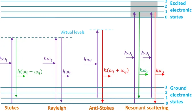
In fact, there are three particular types of light scattering (see in Figure 1.4) clarified by energy change νM between the incident and the scattered photons as shown in the table as below.
Energy change Scattering type Scattering feature
< 10 cm-1 Rayleigh elastic
10 ~10 cm-1 Brillouin inelastic
>10 cm-1 Raman inelastic
Raman scattering is a very weak effect and it is always accompanied with Rayleigh scattering with intensity usually 3–5 orders of magnitude greater. The new components appearing in the spectrum of the scattered radiation at shifted wave
numbers are named Raman lines, and collectively they are referred to the Raman spectrum. The Raman lines at wave numbers less than the exciting wave number are referred to as Stokes lines (νI νM), whereas those appearing at higher wave numbers as anti-Stokes lines (νI νM).
-
Classical treatment of Raman scatteringThe scattering of light could be thought of as the redirection of light that takes place when an electromagnetic wave encounters a material, i.e. as the polarization of incident electromagnetic wave of light. As the electromagnetic wave interacts with the material, the electron orbits within the constituent molecules are perturbed periodically with the same frequency as the electric field of the incident wave. The oscillation or perturbation of the electron cloud results in a periodic separation of charge within the molecules, which is called an induced dipole moment. The classical theory of Raman scattering is based on this induced electric dipoles. The strength of the induced dipole moment P is given by , (1.1)
where is the electronic susceptibility and is the strength of electric field of incident electromagnetic wave. The susceptibility is a second rank tensor that modulated by molecular structure, nature of the bonds, and lattice vibration. Note χ is the susceptibility when the atoms is at equilibrium position, and ∆χ is the modulation by lattice vibration mode. We consider lattice vibration mode as a plane wave with frequency and wave vector , thus the total susceptibility may be expressed as
∆ ∆ · , (1.2)
The electric field of incident electromagnetic wave can be expressed as · , (1.3)
where is the frequency of incident light, is incident wave vector, r is the Figure 1.4. Scattering types classified by frequency shifts
21 position vector in the space.
Thus substituting Eq. (1.2) (1.3) into (1.1) yields the time dependent induced dipole moment,
· ∆ ·
· , (1.4)
The above equation (1.4) reveals that induced dipole moments are created at three different frequencies, namely , , and , which results in scattered radiation at these three frequencies. The first scattered frequency in Eq. (1.4) corresponds to the incident frequency, hence is elastic scattering (Rayleigh), while the latter two frequencies are shifted to lower or higher frequencies and are therefore inelastic processes. The scattered light in these latter two terms is referred to as Raman scattering, with the down-shifted frequency referred to Stokes scattering, and the up-shifted frequency referred to anti-Stokes scattering. It also shows that the Stokes and the anti-Stokes lines have the same energetic distance from the incoming laser light. The positions of these Raman lines are located symmetrically around the Rayleigh scattered component. Hence a peak with Raman origin in a spectrum can always be verified by scanning the anti-Stokes side. Photoluminescence, artifacts from the substrate or stray light have no corresponding component in the anti-Stokes spectrum.
In the Raman scattering process a certain amount of energy is gained or lost by an incident photon with energy (incident) in order to create or annihilate phonons. Energy and momentum are conserved and are given by the following equations:
, (1.5) , (1.6)
here the “minus” sign stands for a phonon excitation (stokes process) while the “plus” sign implies a phonon annihilation (anti-stokes process).
Since the momentum of the incident and scattered photons ( | |
10 ) are small compared with the first Brillouin zone ( 10 ), only excitations with 0 (i.e. long wavelength limit) in the center of Brillouin zone take part in the Raman process. However, in low dimensional solids, when the periodicity is reduced in one or more directions, the momentum conservation is relaxed in the reduced dimensions because the wave vector is not a good quantum number any more. Instead we should discuss the phonons in those directions as folded phonon or confined modes. These modes may be appeared in 2 dimensional superlattices [35].
The electric susceptibility is assumed to change locally with the lattice displacement Q. χ can be thus expanded as a Taylor series in Q and the new term
∂χ/ ∂ , t predicts inelastic Raman scattering. A slightly modified term is known as the Raman tensor. Introducing a unit vector in direction of the lattice
displacement /| |, the Raman tensor can be expressed as ∂χ/ ∂ , t , (1.7)
Assuming and to be the unit vectors of polarization of the incoming and scattered light, respectively, the Raman scattering intensity is proportional to
I | · · | , (1.8)
The Raman tensor is a symmetric second rank tensor if we neglect the difference in frequency of the incoming and outgoing light. The Raman tensor has the same symmetry as the corresponding phonon [36]. Whether a Raman active phonon can be observed under certain experimental conditions regarding the incoming and scattered polarization or not is determined by Eq. (1.8). Using these Raman selection rules the symmetry of the Raman tensor and hence the symmetry of the underlying phonon can be identified by Raman experiments with different scattering geometries. The Raman selection rules of GaN will be detailed in chapter 2.
-
Quantum treatment of Raman scatteringThe quantum treatment to Raman scattering involves the excitation of electron. A photon is scattered by a phonon and its energy is changed by a discrete value. In semiconductors an electron can be excited to an electron-hole pair, to a virtual state or to an exciton. In all cases an electron-hole pair is created which can interact with the lattice. We can treat the Raman quantum process into three steps (see also in figure 1.5).
1. An incoming photon ω creates an electron-hole pair. This state is referred to the transition from the ground state |0 to an excited electronic state |e (photon
Virtual levels 0 2 3 1
Stokes Rayleigh Anti‐Stokes
0 3 1 2 Resonant scattering Ground electronic states Excited electronic states
Figure 1.5. Quantum model of non resonance Raman scattering and resonance Raman scattering
23 absorption).
2. The excited electronic state |e is scattered into another intermediate state |e via the electron lattice interaction and phonon is created or annihilated.
3. The electron-hole pair of state |e decays to the electronic ground state |0 under photon emission ω .
The generalized susceptibility may be described using time-dependent perturbation theory [31]. The dominant term amounts to:
χ , ω , ω · ·V∑ HE P
E E
, , (1.9)
where m is the electron mass, V is the scattering volume, p , p are the Cartesian components of the momentum operators, E , E the energies of the excited electron-hole pair states and HE P the electron-phonon interaction Hamiltonian. It is selected by the unit vectors , of the light polarizations.
In Eq. (1.9) the brackets in the denominator shows that the intensity of Raman scattered signal can be strongly enhanced when the energy of the exciting photons approaches or coincides with the real electronic transition energy. This effect is called Resonance Raman Scattering (RRS) and is due to the coupling of electronic and vibration transition. There are definite advantages compared to normal Raman scattering. First of all, this resonance enhances not only the intensity of the Raman scattering but also reflects basic features from vibration excitations in nanostructures, which is very important particularly for nanostructures because of their small scattering volume and weak Raman features in non resonance condition. Secondly, UV photons can be used to map out the electronic properties of the band, to do photochemical studies by means of RRS. However, the problem might be incurred that the accompanying fluorescence screens the weaker Raman features because of the increased energy absorbed radiation. Thus for a given material with given electronic states the choice of laser line energy for the scattering experiment is one of the most important parameters.
-
Raman experimental instrumentsDue to its sensitivity, high resolution, and non destructive nature, Raman technique is now widely used in many applications across the fields of chemistry, biology, materials science etc. The Raman instruments are fully integrated and come with built-in system intelligence. A descriptive experimental setup of the Raman experiment is shown in Figure 1.6. A laser is used to excite an intense monochromatic light source and some mirrors reflect and guide the light.
The microscope is the heart of the Raman instrument, as it plays the most important role of coupling the light source and the spectral analyzer. Meanwhile, almost all the modern Raman instruments employ a single, wide aperture objective. The laser beam is focused through microscope objectives (x100) down to a 1 µm spot on sample and the scattered light is collected through the same objective. Thus it is so-called µ-Raman and backscattering configuration. A beam splitter is needed to illuminate the sample with the laser beam coaxially, through the objective, and to
transmit the backscattered radiation toward the spectral analyzer. This beam splitter (notch-filter) with a particular dielectric coating is used to cut off the laser line, because the Raman signals are weaker than the elastically reflected laser light (Rayleigh). In other word, the laser light is reflected by the beam splitter, but the inelastically scattered light passes through and is collected by the spectrometer. To separate the collected Raman scattered light into its composite wavelengths, a fixed grating and a detector are employed. The grating disperses the light onto the CCD detector. The spectral distribution of the light is converted into a spatial distribution and can be recorded by the detector. The data analysis is eventually done by a computer program Labspec.
There are two Dilor XY micro Raman Spectrometer in our laboratory clarified by the laser wavelength, visible and ultraviolet excitation. The light source for excitation of sample is an Ar+ /Kr+ laser cooled by water which can provide 514.5 nm and 488 nm exciting lines in visible, 364nm, 351 nm, 335 nm, 300 nm and 275 nm in UV. Laser power can be regulated by using filters. These spectrometers allow us to take backscattering measurements in which the incident beam can be focused by the objective of magnification x40 or x100 with an Olympus microscope. This system allows us to investigate coupling effects between lattice vibrations and certain electronic excitations of nanostructure, especially study of a single nanowire in this work. The resolution of Dilor XY is up to 1 cm-1.
Jobin-Yvon Xplora MV-2000 is another Raman spectrometer which integrates the AFM topography technique. It is equipped with a laser diode which can provide 532 nm, 638 nm and 785 nm exciting lines. A piezoelectric sample stage moving in the x and y directions of µm order allow us to locate the objet studied precisely. The polarization of incident and scattered light analysis are accessible to the Raman study.
With regard to the efficiency of its detection, Jobin-Yvon T64000 allows for the measurements of high resolution Raman spectra and gather weak signals in a relatively short time due to triple modes spectrometer. The excitation is achieved by a coherent Ar+–Kr+ mixed gas ion laser which can provide a great of exciting lines from
25 406.7 nm to 799.3 nm. This system can be utilized in a triple additive or in a triple subtractive mode. An additive mode gives the highest spectral resolution and high linear dispersion in backscattering configuration, whereas a subtractive mode gives a high stray light rejection and allows for collecting low-frequency Raman spectra down to 5 cm-1 in lateral scattering configuration.
1.6 Overview
As shown in the introduction, we will study the structural and vibrational properties of III nitride GaN NWs, GaN/AlN superlattice NWs by Raman scattering.
The structure of this thesis is as follows: chapter 1 describes brief outline of this thesis (the interest and objective), the overview of materials studied and the experimental techniques and setups applied for material characterization. Classical and quantum theory of Raman scattering are introduced in detail. In chapter 2, we introduce briefly the fundamental theory for understanding of this thesis. The basic structure, optical and vibrational properties of wurtzite GaN are presented. In chapter 3, we deal with the GaN NWs ensemble with AFM, SEM and Raman techniques. The growth and morphologies of NWs samples grown by PA-MBE will be described firstly. We investigated the vibrational properties of NWs and detected inelastic scattering by surface related phonon in GaN NWs. This significant role of large surface-to-volume ratio for the optical properties has been investigated experimentally and this study is supported by calculations using an effective dielectric continuum model. From GaN NWs ensemble to individual NW, the Raman results of single NW are discussed in chapter 4. The observed enhancement of A1(TO) mode and a shoulder
in high frequency side are detailed analyzed and compared with DDA-based calculations. Structural properties of GaN/AlN superlattice NWs and core-shell structure NWs are studied by UV Raman measurement. The detailed analysis will be presented in this chapter. In chapter 5, we discuss stress distribution by Raman measurement and finite element method (FEM) modeling on crack free thick GaN layers which were grown on pattern Si(110) substrate by MOCVD. We study the effects of mesa size, GaN thickness and pattern height on the strain distribution. Finally, the results of the thesis are concluded in Chapter 6.
27
References
[1] F. Glas. “Critical dimensions for the plastic relaxation of strained axial heterostructures in free-standing nanowires”, Phys. Rev. B, 74, 121302(R) (2006). [2] E. Ertekin, P. A. Greaney, et al. “Equilibrium limits of coherency in strained nanowire heterostructures”, J. Appl. Phys., 97, 114325 (2005).
[3] Nicolas Thillosen, Kathrin Sebald, et al., “The state of strain in single GaN nanocolumns as derived from microphotoluminescence measurements”, Nano Lett., 6, 704–708 (2006).
[4] R. Agarwal and C. M. Lieber. “Semiconductor nanowires: optics and optoelectronics”, Appl. Phys. A, 85,209 (2006).
[5] Yu Huang, Xiangfeng Duan, Yi Cui, and Charles M. Lieber. “Gallium Nitride Nanowires Nanodevices”. Nano Lett., 2:101–104 (2002).
[6] Reui-San Chen, Hsin-Yi Chen, Chien-Yao Lu, Kuei-Hsien Chen, Chin-Pei Chen, Li-Chyong Chen, and Ying-Jay Yang. “Ultrahigh photocurrent gain in m-axial GaN Nanowires”. Appl. Phys. Lett., 91, 223106 (2007).
[7] Xiangfeng F. Duan, Yu Huang, Ritesh Agarwal, and Charles M. Lieber. “Single nanowire electrically driven lasers”, Nature (London), 421:241–245 (2003).
[8] M. H. Huang, S. Mao, H. Feick, H. Yan, Y. Wu, H. Kind, E. Weber, R. Russo, and P. Yang. “Room-temperature ultraviolet nanowire nanolasers”, Science, 292:1897–1899 (2001).
[9] R. Juza and H. Hahn, “Über die kristallstrukturen von Cu3N, GaN und InN metallamide und metallnitride,” Zeitschrift für anorganische und allgemeine Chemie, vol. 239, pp. 282–287 (1938).
[10] J. I. Pankove, E. A. Miller, and J. E. Berkeyheiser, “GaN Electroluminescent Diodes”, RCA Review, vol. 32, p. 383 (1971).
[11] Shuji Nakamura, Takashi Mukai, and Masayuki Senoh, “Candela-class high-brightness InGaN/AlGaN double-heterostructure blue-light-emitting diodes”, Appl. Phys. Lett., 64, 1687 (1994)
[12] Soon-Jin So et al. “Improvement of brightness with Al2O3 passivation on the surface of InGaN/GaN-based light-emitting diode chips”, Thin Solid Films 516, 2031-2034 (2008)
[13] http://ledsmagazine.com/features/9/6/8
[14] S. Nakamura, “GaN growth using GaN buffer layer”, Jpn. J. Appl. Phys. 30, L1705 (1991).
[15] H. Amano, N. Sawaki, I. Akasaki and Y. Toyoda, “Metalorganic vapor phase epitaxial growth of a high quality GaN film using an AlN buffer layer”, Appl. Phys. Lett. 48, 353 (1986).
[16] X.W. Sun, R.F. Xiao, H.S. Kwok, “Epitaxial growth of GaN thin film on sapphire with a thin ZnO buffer layer bu liquid target pulsed laser deposition”, J. Appl. Phys. 84 , 5776 (1998).
[17] L. Liu and J. H. Edgar, “Substrates for gallium nitride epitaxy”, Materials Science and Engineering R, vol. 37, pp. 61-127 (2002).
[18] “LED breakthrough highlights AlN promise,” Compound Semiconductor, vol. 12, no. 5, pp. 31-32 (2006)
[19] X. Hu, J. Deng, N. Pala, R. Gaska, M. S. Shur, C. Q. Chen, J. Yang, G. Simin, M. A. Khan, J. C. Rojo, and L. J. Schowalter, “AlGaN/GaN heterostructure field-effect transistors on single-crystal bulk AlN,” Appl. Phys. Lett., vol. 82, no. 8, pp. 1299-1301 (2003).
[20] Tiginyanu I M, Ursaki V V, Zalamai V V, Langa S, Hubbard S, Pavlidis D and Foll H, “Liminescence of GaN nanocolumns obtained by photon-assisted anodic etching”, Appl. Phys. Lett. 83, 1551 (2003).
[21] Araki T, Chiba Y, Nobata M, Nishioka Y and Nanishi Y, “Structural characterization of GaN grown by hydrogen-assisted ECR-MBE using electron microscopy”, J. Cryst. Growth 209, 368 (2000).
[22] A. Y. Cho and J. R. Arthur, “Molecular beam epitaxy”, Progress in Solid State Chemistry Volume 10, Part 3, Pages 157-191 (1975).
[23] Theory and Practice, Academic Press, San Diego, California (1999).
[24] J. Ristic, E. Calleja, et al. “On the mechanisms of spontaneous growth of III-nitride nanocolumns by plasma-assisted molecular beam epitaxy”, J. Cryst. Growth 310, 4035 (2008).
[25] O. Ambacher, “Growth and applications of Group III-nitrides”, J. Phys. D: Appl. Phys. 31 2653 (1998).
[26] Koester R, Hwang JS, Durand C, Dang Dle S and Eymery J., “Self-assembled growth of catalyst-free GaN wires by metal-organic vapour phase epitaxy”, Nanotechnology 21,015602 (2010).
[27] Stevie. F. A., Gaianuzzi, L.A. and Preniter, B. I., “The Focused Ion Beam Instrument: in Giannuzzi, L. A. and Stevie, F. A., Introduction to Focused Ion Beams: Theory, Techniques and Practice,” Springer, P13-52 (2005).
[28] D. Wang, C. -C. Tin, J. R. Williams, M. Park, Y. S. Park et al. “Raman characterization of electronic properties of self-assembled GaN nanorods grown by plasma-assisted molecular-beam epitaxy”, Appl. Phys. Lett. 87, 242105 (2005)
[29] T. Kozawa1, T. Kachi1, H. Kano1, Y. Taga1, M. Hashimoto1, N. Koide2, and K. Manabe2, “Raman scattering from LO phonon-plasmon coupled modes in gallium nitride”, J. Appl. Phys. 75 1098 (1994).
[30] Santanu Bhattacharya1, Anindya Datta1, Sandip Dharab ∗ and Dipankar
Chakravorty1 , “Sufrace optical Raman modes in GaN nanoribbons”, J. Raman Spectrosc. 2011, 42, 429–433, (2010)
[31] F. Demangeot and J. Frandon, “Phonon deformation potentials in hexagonal GaN”, Phys. Rev. B 69,155215 (2004)
[32] J. Gleiwe, M. A. Renucci, J. Frandon et al. “Phonon deformation potentials of wurtzite AlN”, J. Appl. Phys. V93, Num. 4, 2003
[33] C. V. Raman. “A new radiation”, Indian Journal of Physics 2,387-398 (1928) [34] C. V. Raman, K. S. Krishnan, “A change of wavelength in light scattering”, Nature 121, 619-620, (1928)
[35]T. Ruf. “Phonon Raman Scattering in Semiconductors, Quantum Wells and Superlattices”, Springer Tracts in Modern Physics. Sringer-Verlag, Berlin, Heidelberg,
29 (1998).
[36] R. Loudon, “Theory of the First-Order Raman Effect in Crystals”, Proceeding Royal Society., 275: 218-232 (1963).
31
Chapter 2 Structure and Properties of III nitrides
2.1 Introduction
Group III nitrides have several remarkable physical properties that make them particularly attractive for Optoelectronic applications. Before the characterization of material by Raman scattering, some basic material properties will be introduced firstly in this chapter. We will describe the crystal structure and vibrational properties in detail.
The band gap energies of III nitrides range from 0.7 eV (InN) to 3.42 eV (GaN) to 6.2 eV (AlN) (see figure 2.1). In view of the available wide range of direct band gaps, GaN alloyed with AlN and InN may cover a continuous range of direct band gap energies throughout much of the visible spectrum well into the ultraviolet
Band gap energy (eV)
Lattice constant (nm)
InN
Figure 2.2 the various binary and ternary materials with the wavelength range indicated.
InN Figure2.1 Band gap of wurtzite InN, GaN, AlN and their alloys versus in plane lattice constant.
wavelengths (shown in figure 2.2). This makes the nitride material attractive for optoelectronic device applications, such as light emitting diodes (LEDs), laser diodes (LDs) and detectors which are active in the green, blue or UV wavelengths [1].
2.2 Crystal Structure of Nitrides
GaN, AlN and their alloys can crystallize in both wurtzite ( -phase) and zincblende ( -phase) structure. Under natural conditions, the thermodynamically stable structure is wurtzite for bulk materials. The metastable zincblende structure could be formed by epitaxial growth of thin films on cubic substrates such as -SiC or MgO (100) substrates. In zincblende form, GaN and InN have direct band gap while AlN is indirect. In this work, samples materials have wurtzite structure. The crystalline structures of both - and -GaN are depicted in Fig.2.3.
As in the zincblende structure, the bonding is tetrahedral. The wurtzite structure is a hexagonal closed-pack lattice. It contains four atoms per unit cell. The space grouping for wurtzite structure is [2] in the Schoenflies notation. It may be generated from the zincblende structure by rotating adjacent tetrahedral about their common bonding axis by an angle of 60 degrees with respect to each other. The basal plane (0001) lattice parameter is depicted by and the axial lattice parameter, perpendicular to the basal plane, is usually described by . The lattice parameters are commonly measured at room temperature by X-ray diffraction (XRD), which happens to be the most accurate one, using the Bragg law. However, inhomogeneity, strain, partial relaxation of strain and structural defects of epitaxial layers on foreign substrates may distort the lattice constants from their intrinsic values. The Table 2.1 lists the intrinsic lattice constants of hexagonal GaN, AlN, InN.
In addition, all III nitrides have partially covalent and partially ionic bonds. We use the concept of fractional ionic character (FIC) which is useful in interpreting many physical phenomena in the crystals [4, 5]. The FIC may be defined for a binary
compound AB as | |/| |, where and are effective
a
a
c
N Ga Zincblende Wurtzite [0001]Figure 2.3 Unit cell of the zincblende cubic and wurtzite hexagonal crystal, the yellow sphere represents Ga atom and the gray N atom.
33 charges on atoms A and B. The FIC values range from zero for a covalent compound (each atom has four electrons) to 1 for an ionic compound (all eight electrons belong to the anion).
Materials InN GaN AlN
a (angstrom) 3.538 3.189 3.11
c (angstrom) 5.703 5.1864 4.98
2.3 Vibration properties
Now we introduce the vibrational properties of nitrides which can be described as mechanical properties. Vibrational modes are very sensitive to crystalline defects, strain, doping and temperature so that the phonon mode frequencies and bandwidths can reflect the important information about the materials. In fact, phonon is a collective excitation in an arrangement of atoms or molecules, which describe a special type of vibration motion, i.e. lattices oscillate at the same frequency. It can be applied in nanostructures to detect for instant crystal quality, doping, defects and strains. In this work, we mainly use the Raman spectroscopic technique to characterize the phonon effects in GaN nanowires.
2.3.1 Crystal symmetry properties
The GaN is uniaxial crystal. It can crystallize in wurtzite structure which has the symmetry and the Brillouin zone (momentum reciprocal space) of the wurtzite structure [6] has been shown in figure 2.4.
The group theory predicts that there are eight sets of phonon modes at the zone Figure 2.4 Brillouin zone of the wurtzite crystal structure.
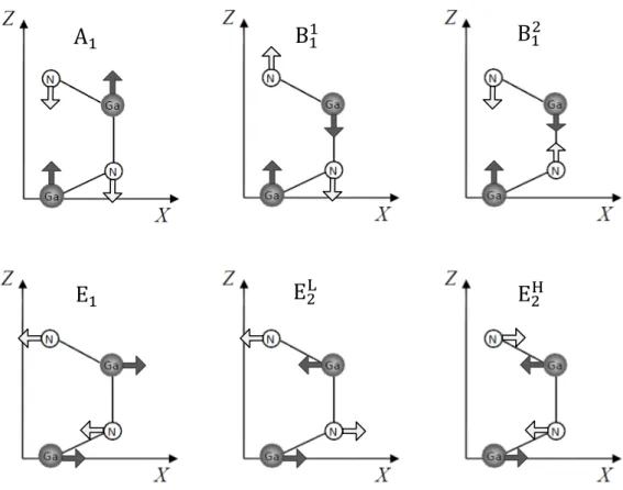
center (Γ point), i.e. 2A1, 2B1, 2E1 and 2E2. Among them, one set of A1 and E1 modes
is acoustic where all the atoms move in the same direction in the unit cell. The remaining six modes A1(Z) + 2B1 + E1(X,Y) + 2E2 are optical modes, where the
X|| 100 , Y|| 010 , Z|| 001 in the parentheses represent the polarization directions. These optical modes in the wurtzite GaN unit cell are depicted in Figure 2.5 based on London’s model [7]. The atomic displacement of A1 and B1 modes is along
the -axis, while that of E1 and E2 is perpendicular to the -axis, meaning on the basal
plane. The A1 and E1 modes are polar vibrations which mean that a net electric dipole
can be set up in each unit cell. This is easily seen from the figure 2.5 because there is a net separation of charge for the A1 and E1 modes but not for the other modes. These
two polar modes are thus not only Raman active but also IR active because the induced dipole for these modes can couple directly with the incident light. The E2 and
B1 modes are non-polar. The E2 mode is only Raman active. B1 mode is neither
Raman nor IR active (silent modes).
2.3.2 Phonon dispersion and energy band
The first-order phonon Raman scattering is caused by phonons with wave vector 0 because of the momentum conservation in the Raman scattering process. The total number of normal vibration modes for a unit cell with atoms is 3 [8]. In the
B
B
E
LE
HA
E
Figure 2.5 Relative atomic displacements in wurtzite GaN unit cell corresponding to the optical modes.
35 long-wavelength limit ( 0) there are 3 acoustic modes and 3 -3 optical modes, where the acoustic modes are simple translational modes. In the wurtzite GaN,
4 and hence there are 9 optical modes. Considering propagation along the -axis in figure 2.5, there is one A1(LA) and two E1(TA) acoustic modes (polarized in
the x and y directions). As to the optical modes, there are one A1(LO), two E1(TO),
one B1(low), one B1(high), two E2(low) and two E2(high) modes, giving 9 optical
mode in total.
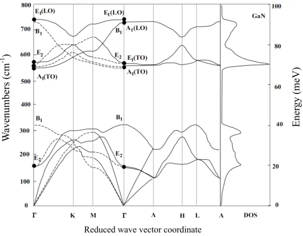
The phonon dispersion curve for wurtzite GaN is shown in figure 2.6 from calculation in [9]. The wave vectors in figure 2.6 correspond to the points in reciprocal space in figure 2.4. Since the momentum of the incident and scattered photons ( | | 2 / 10 ) are very small compared with the first Brillouin zone ( / 10 ), only phonons with 0 can be excited in the first-order Raman process. In the phonon dispersion curves, the phonons with energy at Γ point approaching zero are the acoustic modes. They represent a uniform translation of the entire crystal and it leads to Brillouin scattering with very small frequency shift (< 5 cm-1). They are not investigated in this work.
The optical phonons at Γ point have been labeled in figure 2.6 and frequency shift of Raman active modes at room temperature are listed in Table 2.1. Phonon dispersion curves are measured by inelastic thermal neutron scattering. Second-order
W
avenumbers (cm
-1
)
Ener
gy (meV)
Reduced wave vector coordinate
and disorder induced Raman scattering can give information on the dispersion curves through measurement of the density of phonon states (i.e. the number of phonon states per energy interval).
For the longitudinal optical (LO) modes, the direction of phonon propagation is along the direction of the atomic displacement which gives a macroscopic electric field associated with the oscillation. The transverse optical (TO) mode means that the direction of phonon propagation is perpendicular to the direction of the atomic displacement. We determine the direction of phonon propagation by the angle of incident and scattered light. From the conservation of wave vector , where and describe the wave vector of incident and scattered light, the phonon propagation direction could be determined. If the phonon direction is not exactly parallel or perpendicular to the optical axis ( -axis or -axis), it will give rise to a continuous variation of the phonon frequency between that of the pure A1 and
pure E1 mode. This is the angular dispersion of the frequency in the polar
semiconductor and the mixing of A1 and E1 modes can be expressed by [7, 11, 12, 13]
, (2.1) , (2.2)
where is the angle with respect to the -axis. The calculated angular variation of the optical phonon frequencies of GaN is shown in figure 2.7. We find that the
E2(low) A1(TO) E1(TO) E2 A1(LO) E1(LO)
GaN 114 531.8 558.8 567.6 734 741 AlN 248.6 611 670.8 657.4 890 912 A1(TO) E1(TO) E2 E1(LO) A1(LO) LO-TO splitting A1-E1 splitting A1-E1 splitting Raman Shift (cm -1 ) (Deg)
Table 2.1 Zone center Raman active phonon frequencies (in cm-1) for bulk GaN and
AlN [10] at room temperature.