O
pen
A
rchive
T
OULOUSE
A
rchive
O
uverte (
OATAO
)
OATAO is an open access repository that collects the work of Toulouse researchers and
makes it freely available over the web where possible.
This is an author-deposited version published in :
http://oatao.univ-toulouse.fr/
Eprints ID : 18134
To link to this article : DOI: 10.1109/APEMC.2016.7522751
URL :
http://dx.doi.org/10.1109/APEMC.2016.7522751
To cite this version : Ghfiri, Chaimae and Durier, André and Boyer,
Alexandre and Ben Dhia, Sonia and Marot, Christian Construction of an
Integrated Circuit Emission Model of a FPGA. (2016) In: APEMC 2016
(7th Asia Pacific International Symposium on Electromagnetic
Compatibility & Signal Integrity), 18 May 2016 - 21 May 2016 (Shenzhen,
China).
Any correspondence concerning this service should be sent to the repository
administrator:
staff-oatao@listes-diff.inp-toulouse.fr
Construction of an Integrated Circuit Emission Model
of a FPGA
C. Ghfiri1,2, A. Durier1
(1) IRT Saint-Exupéry, 118 route de Narbonne, CS 44248, Toulouse, France
(2) CNRS, LAAS, 7 avenue du colonel Roche, F-31400 Toulouse, France
chaimae.ghfiri@irt-saintexupery.com
A. Boyer2,3, S. Ben Dhia2,3, C. Marot4
(3) Univ. de Toulouse, INSA, LAAS, F-31400 Toulouse, France
(4) Airbus Group Innovation, BP 13050, Toulouse, France
alexandre.boyer @laas.fr
Abstract— This paper describes the construction flow and the
validation of an equivalent conducted emission model of a complex integrated circuit (a FPGA), based on the ICEM (Integrated Circuit Emission Model) modeling approach.
Keywords— Integrated circuits; Modeling; Conducted emission; ICEM; FPGA.
I. INTRODUCTION
Integrated circuits (ICs) play an important role in electromagnetic compatibility (EMC) issues. In order to anticipate EMC non-compliance risks of electronic applications, the need of predictive models for EMC of ICs increases. These last years, non-confidential equivalent models of ICs have been proposed, such as ICEM [1] or LEECS [2] models, for conducted and radiated emission prediction. Numerous papers have described the construction process of these models and proved their validity [3] [4]. For critical embedded systems with strong requirements in terms of lifetime and robustness, new demands appear such as functional safety or the long-term effect of aging on EMC. As shown in papers as [5], a gradual drift and an increasing variability of the EMC levels may be observed during IC lifetime, especially for deep-submicron (DSM) ICs. In this paper, the construction of a conducted emission model based on ICEM standard for a large digital DSM circuit (a FPGA) is presented. Due to the large number of power supply domains, the modeling of such a device remains challenging. The ultimate goal of this study is to update an equivalent emission model such as ICEM to take into account of variability and aging effect in order to predict their influence on the electromagnetic emission of the circuit. After a brief description of the circuit under test, the methodology, the measurement and simulation tools to build the ICEM model will be presented. Then the different steps of the model development and validation will be described.
II. PRESENTATION OF THE CIRCUIT UNDER TEST
The circuit under test is a XC6SLX9-2FT256 Spartan 6 Xilinx FPGA, manufactured with a CMOS 45-nm process.
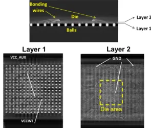
The circuit includes 9152 configurable logic blocks (CLB) and up to 186 user I/Os. The power distribution network of the FPGA is quite complex since it includes six power supply domains: VCCINT dedicated to the CLB (1.2 V), VCCOx (x = 1 to 4) dedicated to the I/O organized in four banks (3.3 V), and VCCAUX dedicated to the JTAG configuration (3.3 V). The circuit is mounted in a Fine pitch Thin Ball Grid Array with 256 balls (FTBGA256). Its internal structure has been analyzed with a 3D X-ray scanner (Fig. 1). This analysis provides valuable information for IC modeling, such as the routing of power supply and ground at package level, presence of inner ground plane, die dimensions, number of bonding wires. GND VCCINT VCC_AUX Balls Die Bonding wires Layer 1 Layer 2 Layer 2 Layer 1 Die area
Fig. 1. X-ray view of the FPGA mounted in a FTBGA256
The conducted and radiated emission of the FPGA depends on the configuration of the logic blocks and the I/O resources. The emission model of the FPGA is built only for some basic configurations. In this study, 5 CLBs are activated by a 19 MHz clock and five output drivers switch simultaneously at 9.5 MHz. The Xilinx ISE Design Suite is used to design, synthesize and place the different configuration on the FPGA. It is essential to check that the same CLB are used between two different tests to ensure measurement repeatability.
This work is supported by the IRT Saint-Exupéry project Robustesse Electronique.
III. DESCRIPTION OF THE TEST BOARD
A specific test board has been designed for the extraction and the validation of the ICEM model of the FPGA. It consists of a six layer board with complete power and ground planes, in a 10˟10 cm format for radiated emission measurements in TEM cell. Several test points have been placed for conducted emissions measurement and characterization of the board impedance. A 1 Ω probe, as defined by the IEC61967-4 [6], has been placed between the ground pins of the FPGA and the ground reference of the test board in order to measure the return current flowing outside the circuit. In addition, 150 Ω probes, as defined by the IEC61967-4 [6], have been connected to the 1.2 V (VCC1.2V probe) and 3.3 V (VCC3.3V probe) power planes of the test board to measure the conducted emission produced by the FPGA activity.
IV. ICEM MODEL
A. General presentation of ICEM model
The Integrated Circuit Emission Model (ICEM) is an IEC standard proposed as IEC 62433-2 for modeling the radiated and conducted parasitic emission produced by an IC at printed circuit board (PCB) level [1]. It can be provided either at the early design stage using electronic design automation (EDA) tools or on an existing IC using measurement tools. In this study, we focus on an ICEM-CE model, dedicated to the prediction of conducted emission (CE). Fig. 2 illustrates the structure of ICEM. A basic ICEM block consists of a set of two components.
The power distribution network (PDN) component presents the characteristics of propagation path of electromagnetic noises; it consists of a passive element network that describes the interaction between the different power supply and ground terminals of an IC, at package and chip level. The Internal Activity (IA) component models the electromagnetic noise source (e.g. current) that originates in switching of active devices in the IC. An IA component is associated to each independent switching part of an IC. The IA blocks are connected to the PDN through internal terminals (IT), while the external terminals (ET) are associated to external physical pads or any electrical connection to the PCB. Measurement points can be placed close to ET in order to sense voltage and currents produced by IA at PCB level.
PDN IA1 IA2 IT1.1 IT1.2 IT2.1 IT2.2 … ET1 ET2 ETN
IC equivalent model (ICEM-CE) PCB model
Connection to the PCB (voltage/current measurement points)
Fig. 2. Illustration of ICEM-CE model
B. ICEM-CE model construction flow
No equivalent model is provided by the circuit manufacturer, which is a usual situation for circuit integrator.
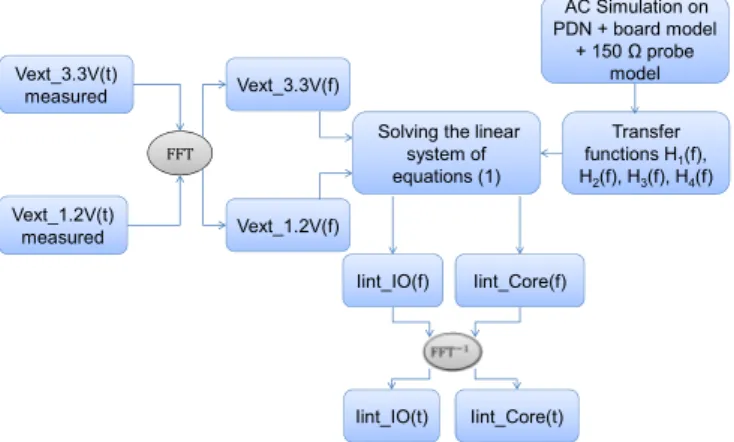
Both parts of the model must be derived from measurement at circuit and board level. Several S-parameter measurements are performed between the different power supply and ground pins of the FPGA, as described in part V. The final PDN model is validated using the comparison with the measurements. The IA construction is based on voltage and/or current measurements in time domain at PCB level produced by the FPGA activity. If the transfer function between the measured current or voltage and the IA component is known, the IA current can be computed. However, in a complex IC such as the FPGA under test, numerous separated internal blocks are activated and are associated to different IA components. With the studied configuration, the noise produced by the FPGA originates from two IA components: one associated to the core, the other to the I/O pads. In order to determine the current profile of both IA components, at least two independent measurement points are necessary. Fig. 3. describes the IA construction flow.
Vext_3.3V(t) measured Vext_3.3V(f) Transfer functions H1(f), H2(f), H3(f), H4(f) FFT Iint_IO(f) AC Simulation on PDN + board model + 150 Ω probe model Vext_1.2V(t) measured Vext_1.2V(f)
Solving the linear system of equations (1)
Iint_Core(f)
Iint_IO(t) Iint_Core(t)
Fig. 3. Construction flow of the IA block
The two 150 Ω probe are used as measurement points for the voltages induced by the FPGA activity on PCB power planes VCC1.2V and VCC3.3V. Additionally, the 1 Ω probe measurement can be used as validation case of the extracted IA components. The measurements of the external voltages across the 150 Ω probe, noted VEXT_3.3V and VEXT_1.2V, are made using a digital oscilloscope with a 2.5 GHz bandwidth. To obtain the current profiles in time domain of both IA blocks (Iint_IO and Iint_Core), the external voltages are first expressed in the frequency domain using the Fast Fourier Transform (FFT). Then, the current profiles of IA components are calculated by solving the linear system of equations, as given by (1). H1, H2, H3 and H4 are the transfer functions between the 150 Ω probes and the IA component currents. They are calculated by SPICE small-signal analysis based on the circuit PDN and board model.
( )
( )
( )
( )
+
=
+
=
Core IO V ext Core IO V extI
f
H
I
f
H
V
I
f
H
I
f
H
V
int 4 int 2 2 . 1 _ int 3 int 1 3 . 3 _.
.
.
.
(1)V. CONSTRUCTION OF THE PDN BLOCK
Several S-parameter measurements have been performed with a VNA between the different power and ground pins of the FPGA in order to extract the complex impedance between
these different accesses. The FPGA is mounted on a small test boards with coplanar GS probe prints placed as close as possible to power supply and ground pins of the FPGA.
From the knowledge of the different power supply domain of the FPGA and the internal routing of the package, the topology of an equivalent electrical model is proposed. The values of the R, L, C of the model are adjusted from the measurement. The model is presented in Fig. 7. In this model, a 130 pF distributed capacitance has been added to model the common mode impedance between the package and the PCB. Fig. 4 presents a comparison between the measurement and the simulation of the impedance seen from the power pinsVCC0 when the VSS pins are shorted or left open. A good agreement between the measured and the simulated impedance is ensured up to 1 GHz.
Fig. 4. Comparison between measurement and simulation of the impedance between Vcc0 and Vss_GND
VI. CONSTRUCTION OF THE IA BLOCK
A. Test board modeling
The modeling of the board is performed using the electromagnetic simulation software CST PCB Studio. The board model is created by importing the design files (ODB++). For this simulation, 8 ports are defined: four ports are placed on the measurement points. Four other ports are placed as close as possible to the FPGA footprint on the power planes (1.2 V /3.3 V) and on the 1 Ω probes, as shown in Fig 5. The 3D FE FD (Finite Element Frequency Domain) solver
based on the finite elements method was chosen for the board modeling because it is capable to analyze the entire PCB design accurately. The number of mesh cells reaches 5,198,095 and the simulation lasts 30 minutes for the frequency range 10 KHz – 2.5 GHz. An example of the obtained results is given in Fig. 6. and shows a good correlation between the measured and simulated impedance profiles.
Ports defined close to the FPGA on VCC3.3V,
VCC1.2V, VSSIO, VSSCORE
Decoupling Capacitors
FPGA Area Ports defined at the measurement points on
VCC3.3V, VCC1.2V and the two connectors
of the 1Ω probe
Fig. 5. Ports definition for modeling the board using CST Studio
Fig. 6. Comparison between measurement and simulation of the input impedance seen from VCC3.3V (port 1) and VCC1.2V (port 2) power planes
B. Internal current profile extraction
In order to obtain the current model, it is mandatory to define a given activity. The configuration used for the extraction of the current is detailed in part II. The modeling of the internal current relies on the measurement of the external voltage and/or current consumed by the IC. Fig 8 shows the measurement in frequency domain of the external voltage on the VCC1.2V supply using the 150 Ω probe.
Using ADS simulator, an AC simulation is performed on the model including the FPGA, the board and the 150 Ω probes. Fig 9 presents an example of the transfer function H3 obtained as described in part IV. The same methodology is followed for the measurement of the external voltage VEXT_3.3 V and the simulation of the transfer functions H1, H2 and H4. By solving the linear system of equations (1), the currents obtained are given by Fig 10.
Fig. 8. Spectrum of the external voltage measured on VCC1.2V using the 150 Ω probe
Fig. 9. Transfer function H3 obtained by AC simulation
Fig. 10. The internal currents calculated on the power supply planes 3.3 V and 1.2 V
C. Validation of the internal current extraction methodology
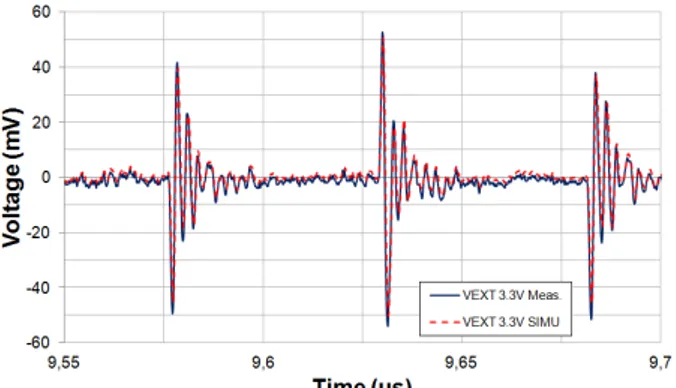
The construction of the internal current methodology is validated by a transient simulation using the currents calculated. Figs. 11. and 12. show a good correlation between the external voltages measured and simulated on the power supply planes 3.3 V and 1.2 V.
Fig. 11. Comparison between the external voltage measured and simulated on VCC3.3 V
Fig. 12. Comparison between the external voltage measured and simulated on VCC1.2 V
References
[1] IEC62433-2 - EMC IC modelling – Part 2: Models of integrated circuits for EMI behavioural simulation – Conducted emissions modelling (ICEM-CE) - Edition 1.0, October 2008, IEC.
[2] Y. Saito, M. Yasuhara, Y. Funato, U. Paoletti, O. Wada, "LEECS-core Model including Inter-Block Coupling for an LSI with Multiple Power-Supply Pins", EMC'09 Kyoto, IEICE, 2009.
[3] S. Serpaud, J. L. Levant, Y. Poiré, M. Meyer, S. Tran, " ICEM-CE extraction methodology", EMC Compo 2009, Nov. 17-19, 2009, Toulouse, France.
[4] K. Iokibe, Y. Toyota, "Estimation of Data-Dependent Power Voltage Variations of FPGA by Equivalent Circuit Modeling from On-Board Measurements", EMC Compo 2013, Dec.15 – 18, 2013, Nara, Japan [5] A. Boyer, S. Ben Dhia, “Characterization and Modeling of Electrical
Stresses on Digital Integrated Circuits Power Integrity and Conducted Emission”, EMC Compo 2013, Dec.15 – 18, 2013, Nara, Japan. [6] IEC 61967-4 – edition 1.1: Integrated circuits - Measurement of
electromagnetic emissions, 150 kHz to 1 GHz - Part 4: Measurement of conducted emissions – 1 Ω/150 Ω direct coupling method, 2006-07. 370