O
pen
A
rchive
T
OULOUSE
A
rchive
O
uverte (
OATAO
)
OATAO is an open access repository that collects the work of Toulouse researchers and
makes it freely available over the web where possible.
This is an author-deposited version published in :
http://oatao.univ-toulouse.fr/
Eprints ID : 18288
To link to this article :
DOI: 10.1109/EMCEurope.2017.8094792
URL :
http://dx.doi.org/10.1109/EMCEurope.2017.8094792
To cite this version :
Ghfiri, Chaimae and Durier, André and Boyer,
Alexandre and Ben Dhia, Sonia A new methodology to extract the ICEM-CE
internal activity block of a FPGA. (2017) In: EMC Europe, 4 September
2017 - 8 September 2017 (Angers, France).
Any correspondence concerning this service should be sent to the repository
administrator:
[email protected]
A new methodology to extract the ICEM-CE
internal activity block of a FPGA
Ghfiri
1,2, A. Durier
1,
(1) IRT Saint-Exupéry, 118 route de Narbonne, CS 44248, Toulouse, France
A. Boyer
2,3, S. Ben Dhia
2,3(2) CNRS, LAAS, 7 avenue du colonel Roche, F-31400 Toulouse, France
(3) Univ. de Toulouse, INSA, LAAS, F-31400 Toulouse, France
alexandre.boyer @laas.fr
Abstract— This paper describes a new methodology of
construction of the internal activity block of an ICEM-CE model of an FPGA based on a predictive approach using the estimation tools of the dynamic power and the static timing proposed by the manufacturer of the integrated circuit.
Keywords— Integrated circuits; Internal Activity; Conducted emission; ICEM; FPGA, Dynamic power.
I. INTRODUCTION
The combined use of IEC 62433-2 Integrated Circuit Emission Model – Conducted Emissions (ICEM-CE) standard [1] and of Printed Circuit Board (PCB) model allows the end-user to predict the CE at equipment level. The ICEM-CE model consists of two parts: the Internal Activity (IA) block consisting of a set of equivalent current sources reproducing core and Input / Output (IO) switching noise and the Passive Distribution Network (PDN) block consisting of the noise’s path through the die and package interconnects to the IC’s pins. While IO switching noise could be accurately predicted using Input output Buffer Information Specification (IBIS) model [2], the construction of the IA block dedicated to core noise modelling remains a challenging task especially for complex ICs.
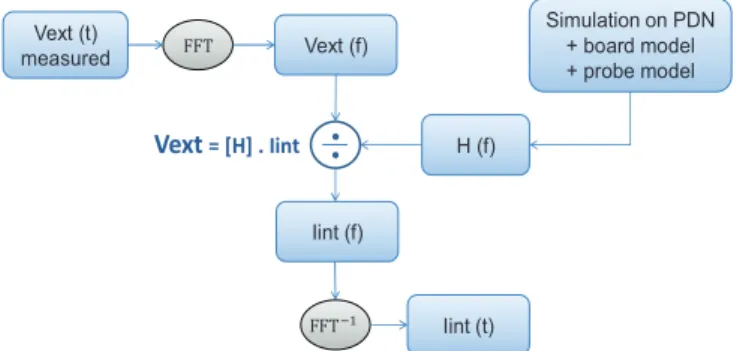
Several methods have been proposed for the construction of the IA block of the core. As proposed by the ICEM-CE model, the IA block could be extracted from IEC 61967- 4 [3] measurements using an inverse method to recalculate internal currents sources [4] as described by Fig. 1.
Vext (t) measured Vext (f) H (f) !!" Iint (f) !!"#$ Iint (t) Simulation on PDN + board model + probe model Vext= [H] . Iint
Fig. 1. IA core block construction workflow using inverse method calculation.
The main drawback of this approach is that the IA extraction result depends on the PDN measurement and is extremely sensitive to any measurement error. The IA Core block can also be constructed from the simulation of the transistors netlist, the transistor model library and the standard cell models [5][6][7]. However, this approach requires considerable simulation time and relies on unavailable data for end-users.
The IA block may be estimated from basic technological information and IC characteristics (e.g. CMOS technological node, number of logic gates, die surface…) using tools as ICEM expert module in IC-EMC software [8]. The IA is roughly estimated from the floor planning definition of the circuit without exact information about the circuit and the main drawbacks of this approach are the weak precision and the lack of knowledge of the end-user IC configuration.
For some IC families such as Field Programmable Gate Array (FPGA), design tools provide to the end-users accurate estimation of the average dynamic power estimation from post-placement and routing simulations of a given configuration. Moreover, some advanced FPGA design tools are able to determine the instantaneous dynamic power consumption from a vector-based simulation, which allows the calculation of the time-domain profile of the dynamic current consumption and thus a precise extraction of IA core block [9]. However, this type of approach requires long simulation times, whose results are dependent on the input test vectors. To overcome this issue, we propose to estimate the IA block of a FPGA from vectorless power estimation and static timing analysis applied on post-placed and routed design. Compared to the vector-based approach, this solution is able to provide a good estimation of the IA block in a very short time, without additional steps in the FPGA design flow, and from a reduced set of data. Moreover, the proposed approach is able to take into account the random activity of the circuit. The proposed method can be applied to any FPGA end-user application or to any circuits developed with design tools providing necessary information.
In this paper, the IA core block construction methodology is applied to a XILINX XC6SLX16-FT256 Spartan 6 and is validated through several case studies. Its accuracy is evaluated through comparison between CE measurements and simulations. The first chapter is devoted to the presentation of
the IA core block construction methodology. Secondly, the case studies are exposed. Finally, the last chapter is dedicated to the validation of the methodology through the different case studies.
II. INTERNAL ACTIVITY CONSTRUCTION PRINCIPLE
The CE of a synchronous digital circuit is related to the instantaneous current consumption, i.e. the charge transfer from the power supply to internal logical gates synchronized by a clock signal. The ICEM-CE model relies on one or several current sources connected to an equivalent model of the power distribution network that conducts the noise produced by the circuit switching activity to the IC’s pins. The relevance of the model depends on:
• The accuracy of the PDN block. This block is supposed independent of the instantaneous activity of the circuit. Numerous publications present reliable methods to extract a model of a circuit PDN so that we consider that the PDN is known in the following paragraphs.
• The accuracy of the IA block. Multiple variable parameters affect this block, such as the clock frequency, the power supply voltage or the internal activity of the circuit.
Before presenting our IA core block construction methodology, a preliminary question is this: is it necessary to determine precisely the time-domain waveform of the instantaneous current consumption to obtain an acceptable CE prediction? In the next paragraphs, we will demonstrate that the answer is no and that only two criteria must be respected to obtain a reliable prediction of CE.
A. Influence of the instantaneus current consumption waveform on emission spectrum
In digital synchronous circuits, current consumption appears mainly during transitions from logical state 0 to 1. Thus, the time domain profile of the instantaneous current is a periodic series of short pulses; its period is equal to the clock period Tc. As explained in [9], the power supply noise can be predicted if the charge consumed at each clock transition is determined correctly. The waveform of the current i(t) delivered by the IA block must reproduce this charge quantity, given by:
=
!
τ( )
0
i
t
dt
q
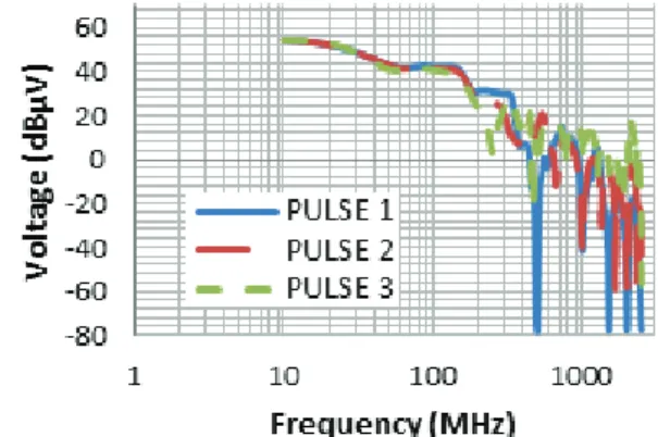
(1) Where q is the transferred charge during a clock cycle and ! is the duration of the charge transfer or the current pulse. Moreover, to reproduce the CE spectrum, the duration ! of the charge transfer must be also known. In order to illustrate this principle, let consider the three basic periodic pulsed waveforms presented in Fig. 2, which model the dynamic current consumption of a digital circuit. The clock frequency is 10 MHz. The pulse durations are identical; their amplitudes are chosen such as the transferred charge is identical. These current waveforms are generated by a current source and form an IA block which is connected to the PDN block representative of a large digital IC. The voltage across a 1 " resistor connected to the Vss pins of the circuit is simulated for each waveform. Fig. 3 presents a comparison of the simulated voltages using the different waveforms in frequency domain. In spite of some differences in high frequency(around the nulls of the spectral envelop), the envelopes of the spectra are very close, providing nearly identical estimation of the CE noise.
Fig 2. Three basic pulsed waveforms to model the dynamic current consumption of a circuit
Fig 3. Comparison between the simulations using the different shapes of IA with a 1 # probe
Whatever the waveform of the instantaneous current consumption, if the transferred charge and transfer duration are respected, an acceptable estimation of the CE can be obtained. This is the purpose of our methodology.
B. Presentation of the IA construction methodology for a FPGA circuit
The charge quantity transferred at each clock cycle can be determined from measurements or the evaluation of the average dynamic power consumption Pdyn_avg by a design tool.
It is given by (2): DD L N i C avg dyn
F
i
q
i
V
P
=
"
⋅
=)
(
).
(
1 _α
(2)where N is the number of internal logical nodes or signals in the circuit, $(i) is the average number of transitions on signal i per clock cycle (toggle rate), qL(i) is the quantity of the
charge associated to signal i, VDD is the power supply voltage
and FC is the clock frequency of the circuit. For its Spartan 6
family, Xilinx provides inside its ISE software the Xilinx Power Analyzer (XPA) module which gives a detailed estimation of the power consumption in the clock tree, the signals and logic blocks, and the IOs after a post-placement and routing simulation. XPA also gives a vectorless estimation of the toggle rates and average dynamic power of all the internal logic signals. From these estimated parameters, the average quantity of charge transferred during a clock cycle QL
can be calculated. For each clock period TC, the internal
activity produces the same quantity of the charge as given by the formula (3), where Iavg is the average dynamic current
consumption.
( ) ( )
avg C N i L Li
q
i
I
T
Q
=
"
=
⋅
=1α
(3)ISE Xilinx tool performs a static timing analysis which gives a detailed report about the slack and the data path delays at the fast and slow PVT (Process/Voltage/Temperature) corners. For the construction of the IA, the pulse duration ! is considered to be the median value of the interval whose boundaries are the maximum data path !max and the minimum
data path !min given by the static timing report (4). The average
dynamic current associated to a periodic pulsed waveform i(t) is calculated using (5).
2
min maxτ
τ
τ
=
+
(4)dt
t
i
T
I
C avg=
⋅
!
⋅
τ 0)
(
1
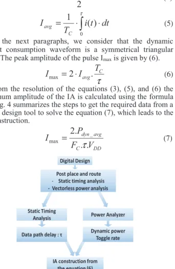
(5)In the next paragraphs, we consider that the dynamic current consumption waveform is a symmetrical triangular pulse. The peak amplitude of the pulse Imax is given by (6).
τ
C avgT
I
I
max=
2
⋅
.
(6) From the resolution of the equations (3), (5), and (6) the maximum amplitude of the IA is calculated using the formula (7). Fig. 4 summarizes the steps to get the required data from a FPGA design tool to solve the equation (7), which leads to the IA construction. DD C avg dynV
F
P
I
.
.
.
2
_ maxτ
=
(7) Digital Design Post place and route- Static timing analysis
- Vectorless power analysis
Static Timing
Analysis Power Analyzer
Data path delay : ! Dynamic power Toggle rate
IA construction from the equation (6)
Fig 4 . Construction workflow of the Internal Activity block for FPGA circuit
The proposed workflow of construction of the IA is based on the average dynamic power consumption, hence, the approach proposed is deterministic; the amplitude of the IA is constant at each clock cycle. In practical cases, the IA profile is random due to the variation of the toggle rate and the power consumption of the active logic blocks. Thus, the peak-to-peak amplitude of the IA in the time domain could be under estimated and the envelope of the emission spectrum
inaccurate. In the next part, an alternative approach is proposed for the construction of a random IA.
C. Statistical method for construction of a random IA
The construction of a random IA block is possible with a vector based simulation [9] but this may require long simulation time. However, the power analysis tool XPA gives the switching probability of each logic block of the circuit. The variability of the switching activity around its mean value can be estimated in a short time simulation. For the construction of a random IA, a methodology based on the statistical distribution of the transferred charge per clock cycle is proposed.
XPA tool gives a detailed report about the dynamic power consumption and the toggle rate for the routed signals and the logic blocks. With these data, it is possible to calculate the probability density function (pdf) of switching of each logic block of the circuit and thus the pdf of the transferred charge to each logic block per clock cycle. Although the logic states of each logic block are partially dependent, we neglect these interdependencies since they cannot be determined through the vectorless estimation of XPA. Considering that each logic block of the circuit switches independently from the others, the pdf of the transferred charge to the circuit is the convolution product of the pdf of the transferred charge of each logic block and the toggle rate. Statistical parameters such as the average and standard deviation can be calculated, and the most representative statistical law can be determined. In practice, due to the large number of switching logic nodes, the distribution tends to be Gaussian. Under this assumption, the probability that a logic block i transfers a charge quantity q(i) per clock cycle is given by the toggle rate $(i). Hence, the average transferred charge quantity
q
(i
)
for each logic block is calculated using the equation (8). Considering the charge quantity q(i) as a random variable, the expected varianceσ
i2 is given by the formula (9), allowing the calculation of the pdf of each logic block i, where N is the number of logic states, for a binary case N=2.
q
L( )
i
=
α
(
i
)
⋅
q
L( )
i
(8)"
(
( )
( )
)
=−
⋅
=
N j L L ij
q
j
q
i
1 2 2)
(
α
σ
(9)The pdf of the transferred charge to the circuit follows the normal distribution
(
, 2)
σ L Q
N , where
Q
L is the average transferred charge quantity (10) andσ
2its variance (11).
"
( )
==
N i L Lq
i
Q
1 (10)"
==
N i i 1 2 2σ
σ
(11)Finally, in order to generate a SPICE compatible IA source, a series of random charge quantity Q(k) is generated at each clock cycle according to the previous pdf. Considering a
symmetric triangular pulse, the amplitude
I
max(
k
)
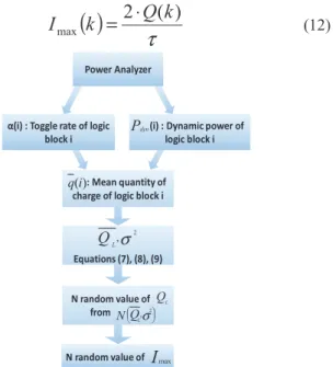
of the IAis given by the expression (12), where k is the number of generated points. The IA is then modelled using a current source based on PWL file. Fig. 5 summarizes the approach of construction of the IA using the statistical distribution.
( )
τ
)
(
2
maxk
Q
k
I
=
⋅
(12) Power Analyzer Equations (7), (8), (9) : Mean quantity of charge of logic block i "(i) : Toggle rate of logicblock i
(i) : Dynamic power of logic block i Pdyn ) (i q σ2 , QL N random value of from QL # $ % & ' ( σ2 , Q N L
N random value of
Imax
Fig 5 . Workflow of the IA construction using the statistical approach
III. PRESENTATION OF THE CASE STUDIES A. The circuit under test
The circuit under test is a XC6SLX16-FT256 Spartan 6 Xilinx FPGA, manufactured with a CMOS 45-nm process. The circuit includes 9152 configurable logic blocks (CLB) and up to 186 user IOs, it is mounted in a Fine pitch Thin Ball Grid Array 256 balls (FTBGA256). The internal structure of this component is complex; it comprises six different power supply planes: VCCINT dedicated to the CLB (1.2 V), VCCOx (x =
1 to 4) dedicated to the I/O organized in four banks (3.3 V), and VCCAUX dedicated to the JTAG configuration (3.3 V), and
a ground plane for the VSS pins.
B. Description of the test board
A specific test board has been designed for the external voltage measurements and the validation of the constructed Internal Activity. It consists of a six layer board with complete power and ground planes compliant to the IEC 61967-1 [10]. Several test points have been placed for CE measurements and characterization of the board impedance. A 1 # probe, as defined by the IEC 61967-4 standard has been placed between the ground pins of the FPGA and the ground reference of the test board in order to measure the return current flowing outside the circuit. Models of the PDN of the FPGA and of the test board have been constructed from S parameter measurements and electromagnetic simulations and previously validated [4].
C. Configurations
The construction of a predictive internal activity of the FPGA is performed for a given activity. The workflows
presented in part II are verified for different case studies of basic synchronous digital designs. . The clock frequency is set to 16 MHz for the different case studies. Fig. 6 shows the structure of the first case study: a delay line. For optimum dynamic power consumption, 90 delay lines have been cascaded in series, each delay line has N = 100 inverters. Due to its regular structure, its dynamic power consumption is deterministic, i.e the number of switching gates remains identical at each clock transition.
CLK %&'( ) * !+,-.!+/-* !+,-.!+/-01,23456457
Fig 6. Structure of a delay line
As another validation case, a configuration with a random number of switching gates is tested, with a Pseudo Random Number Generator (PRNG) blocks. The structure of the 5-bit PRNG is presented in Fig. 7. 200 identical PRNG have been cascaded in parallel to maximize the dynamic power consumption. For the different cases, no output buffer is switching, hence, the 1 # measurements and simulations shows only the contribution of the internal logic blocks and the clock tree activity of the FPGA. Table 1 summarizes the dynamic power consumption, data path delay and the average toggle rate collected from the estimation tools of Xilinx.
CLK * !+,-.!+/-* !+,-.!+/-* !+,-.!+/-* !+,-.!+/-*
!+,-.!+/-Fig 7. Structure of the 5-bit PRNG
TABLE I. ESTIMATED PARAMETERS FOR THE DIFFERENT CONFIGURATIONS
Configuration
Dynamic Power (mW)
Data path delay (ns)
Average toggle rate
(%)
Logic Clock Logic Clock
Delay Line 24 1,5 40 0,75 100 5-bit PRNG 3,11 1,5 1,5 0,75 38,75
IV. CONSTRUCTION OF THE INTERNAL ACTIVITY BLOCK A. Case study 1: delay line
The first case study (delay line) has a toggle rate of 100 % because all the signals are switching at the rising edge of the clock. The clock tree presents non-negligible dynamic power consumption, its toggle rate is about 200 %, and hence, the signals representing the clock tree consumes energy at both rising and falling transitions of clock signal. Therefore, the internal activity of the clock tree is separated from the internal activity of the signals and the logic blocks. As shown in Fig. 8, two current sources are used to represent the activity of the clock, and one current source represents the activity of the signals and logic blocks. The IA waveform is supposed as a symmetric triangular pulse. The parameters are calculated
from the resolution of the equations given in the previous chapter.
VCC
VSS
I = 89: Delay = ;<=>/2 ?@= !ABCD) ?E= !<=>D) T = ?ABC I = 9: Delay = 0 ?@= !ABCD) ?E= !<=>D) T = ?ABC I = 9F Delay = !<=> ?@= !BGHIAD) ?E= !BGHIAD) T = ?ABCIA clock
IA logic
Fig 8. Internal Activity of the core block
The constructed internal activity block is combined to the PDN and the board equivalent model. A transient simulation using ADS is performed to simulate the CE produced by the FPGA and measured through a 1 # probe. The time-domain simulation and measurement results are compared in Fig. 9. The simulated peak-to-peak amplitude of the voltage fluctuation is equal to 9 mV and presents a good correlation with the measured amplitude equal to 11 mV.
Fig 9. Comparison between the measured and simulated external voltage using a 1 # probe in the time domain generated by the delay line configuration
Fig. 10 shows a comparison between the measured and simulated external voltages with a 1 # probe in the frequency domain. In general, the comparison presents a good correlation between the measured and the simulated spectrum with a RMS error of 5,15 dB. Simulation predicts that the frequency content of CE falls down above 1.2 GHz. This is confirmed by measurements.
Fig 10. Comparison between the measured and simulated external voltage using a 1 # probe in the frequency domain of the delay line configuration
B. Case study 2: 5-bit PRNG
1) Modelling with the deterministic approach
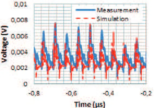
The case of the PRNG presents pseudo-randomly switching bits every clock cycle. Thus, the dynamic power consumption will vary following the variation of the toggle rate of the active logic blocks. As a first approach, an IA is constructed following the deterministic approach for the CE simulation. Fig. 11 shows the comparison in the time domain between the simulation and the measurement of the external voltage fluctuation using a 1 # probe. The simulated peak-to-peak amplitude of 5,2 mV under-estimates the measured maximum peak-to-peak amplitude of 7 mV. Although the simulation gives an approximate estimation of the mean amplitude, it does not represent the variable character of the CE.
Fig 11. Comparison between the measured and simulated external voltage using a 1 # probe in the time domain of the 5-bit PRNG using the deterministic approach
Fig. 12 presents the Fast Fourier Transform (FFT) of the previous comparison. The first harmonics are under-estimated, but globally, the simulated CE shows a good correlation with the measurement, the RMS error is 5,89 dB.
Fig 12. Comparison between the measured and simulated external voltage using a 1 # probe in the frequency domain of the 5-bit PRNG using the deterministic approach
2) Modelling with the statistical approach
To improve the relevance of the results of the simulated CE in the time domain presented in the previous part, a random IA is constructed using the statistical method. Fig. 13 shows the simulated and the measured external voltages using a 1 # probe. The simulated maximum peak-to-peak amplitude of the voltage fluctuation of 7,1 mV allows the prediction of
the maximum peak-to-peak amplitude of 7 mV with a good precision. In general, the simulated time domain profile reproduces the random behavior of the CE with a good approximation.
Fig 13. Comparison between the measured and simulated external voltage using a 1 # probe in the time domain of the 5-bit PRNG using the statistical approach
Fig. 14 presents the comparison of the measured and simulated external voltages using a 1 # probe in the frequency domain. The envelope of the simulated CE shows a good correlation with the measured envelop. The RMS error in this case is about 5,26 dB.
Fig 14. Comparison between the measured and simulated external voltage using a 1 # probe in the frequency domain of the 5-bit PRNG using the statistical approach
V. CONCLUSION
In this paper, a new methodology of construction of the IA block for ICEM-CE model of FPGA circuits has been presented. The main idea is that whatever the internal dynamic current waveform is, the simulated conducted noise will not vary much if the transferred charge and the pulse duration are determined correctly. Also, the dynamic current of an integrated circuit depends mainly on three parameters: the
dynamic power consumption, the toggle rate and the clock and data path delay. Using the estimation tools given by the manufacturers of FPGA, these parameters can be extracted rapidly and without extra steps in the FPGA design flow, and allow the modelling of the IA following two different approaches: The deterministic approach and the statistical approach. Different validation cases have been discussed and generally the comparisons between the measured and simulated CE spectrum present a RMS error calculated for the clock harmonics less than 6 dB, and globally the envelope of the spectrum is predicted with a good approximation. This error can be related to the extraction of the PDN block of ICEM-CE model, the assumptions of our proposed methodology and to measurement accuracy. Future works will be carried out to better evaluate the intrinsic error of the proposed method.
The methodology presented in this paper is adapted to FPGA and other integrated circuits when the manufacturer provides power and delay estimation tools to IC end-users. On the other hand, the principle is still adapted to ICs when the manufacturers do not provide estimation tools but the needed parameter should be extracted from the measurement.
References
[1] IEC62433-2 - EMC IC modelling – Part 2: Models of integrated circuits for EMI behavioural simulation – Conducted emissions modelling (ICEM-CE) - Edition 1.0, October 2008, IEC.
[2] C. Ghfiri, A. Durier, A. Boyer, S. Ben Dhia, C. Marot, “Construction d’un modèke ICEM pour prédire l’émission électromagnétique d’un FPGA”, CEM Rennes 2016, Rennes, France.
[3] IEC 61967-4 – edition 1.1: Integrated circuits - Measurement of electromagnetic emissions, 150 kHz to 1 GHz - Part 4: Measurement of conducted emissions – 1 "/150 " direct coupling method, 2006-07. [4] C. Ghfiri, A. Durier, A. Boyer, S. Ben Dhia, C. Marot "Construction of
an Integrated Circuit Emission Model of a FPGA", APEMC 2016, Shenzhen, China.
[5] B. Vrignon, S. Delmas Bendhia, E. Lamoureux, E. Sicard, "Characterization and Modelling of Parasitic Emission in Deep Submicron CMOS", IEEE Trans on EMC, vol 47, no 2, May 2005 [6] Hyun Ho Park, Seung-Hyun Song, Sang-Tae Han, Tae-Sun Jang,
Jin-Hwan Jung, Hark-Byeong Park, "Estimation of Power Switching Current by Chip-Package-PCB Cosimulation", IEEE Trans on EMC, vol 52, no 2, May 2010
[7] J. P. Leca, N. Froidevaux, P. Dupré, G. Jacquemod, H. Braquet, "EMI Measurements, Modelling, and Reduction of 32-Bit High-Performance Microcontrollers", IEEE Trans on EMC, vol 56, no 5, October 2014 [8] E. Sicard, L. Bouhouche, "Using ICEM model Expert for TC1796
Emission", IC-EMC application note, www.ic-emc.org
[9] Liehui Ren, Tun Li, Sandeep Chandra, Xiaohe Chen, Hemant Bishnoi, Student Member, Shishuang Sun, Peter Boyle, Iliya Zamek, Jun Fan, Daryl G. Beetner, Senior Member, James L. Drewniak, "Prediction of Power Supply Noise From Switching Activity in an FPGA", IEEE Trans on EMC, vol 56, no 3, June 2014
[10] IEC 61967-1- edition 1.0 Integrated circuits - Measurement of electromagnetic emissions, 150 kHz to 1 GHz - Part 1: General conditions and definitions, 2002.
This work is supported by the IRT Saint-Exupery Electronics Robustness project sponsored by Airbus Operations, Airbus Group Innovations, Continental Automotive France, Hirex Engineering, Nexio, Safran Electrical & Power, Thales Alenia Space France, Thales Avionics and the French National Agency for Research (ANR)