HAL Id: hal-02140638
https://hal.archives-ouvertes.fr/hal-02140638
Submitted on 27 May 2019
HAL is a multi-disciplinary open access
archive for the deposit and dissemination of
sci-entific research documents, whether they are
pub-lished or not. The documents may come from
teaching and research institutions in France or
abroad, or from public or private research centers.
L’archive ouverte pluridisciplinaire HAL, est
destinée au dépôt et à la diffusion de documents
scientifiques de niveau recherche, publiés ou non,
émanant des établissements d’enseignement et de
recherche français ou étrangers, des laboratoires
publics ou privés.
Simulation of Coupled Channels
C. Siviero, R. Trinchero, S. Grivet-Talocia, S. Stievano, G. Signorini, Mihai
Telescu
To cite this version:
C. Siviero, R. Trinchero, S. Grivet-Talocia, S. Stievano, G. Signorini, et al.. Constructive Signal
Ap-proximations for Fast Transient Simulation of Coupled Channels. IEEE Transactions on Components
Packaging and Manufacturing Technology Part B, Institute of Electrical and Electronics Engineers
(IEEE), 2019, 9 (10), pp.2087 - 2096. �10.1109/TCPMT.2019.2917773�. �hal-02140638�
Constructive Signal Approximations for Fast
Transient Simulation of Coupled Channels
C. Siviero, R. Trinchero, Member, IEEE, S. Grivet-Talocia, Fellow, IEEE, I. S. Stievano, Senior Member, IEEE,
G. Signorini, Member, IEEE, M. Telescu Member, IEEE
Abstract—This paper addresses the problem of fast transient simulation of high-speed coupled channels driven by transceivers that include Transmitter Feed-Forward Equalization (TX-FFE). Practical circuit hardware implementations of such drivers may not be correctly represented by industry standard algorithmic modeling interfaces, which are usually based on ideal digital finite impulse response filters. In particular, slow transients may arise when aggressive FFE is activated and particular switching sequences significantly stress local voltage regulators integrated in the output buffers. In this paper, we model this effect using a constructive hierarchical approximation of the analog waveforms that form a linearized vector Thevenin or Norton representation of the driver. This representation enables the accurate simulation of coupled channels including both differential and common-mode signals. Analog waveforms at the receiver input are readily obtained by standard time-frequency transformations, while including channel characteristics and any additional linear equalization block, if present. This proposed framework is compatible with industry-standard Algorithmic Modeling Interfaces (AMI), extending their scope to coupled channels with non-ideal TX-FFE circuit blocks. Eye diagrams and transient waveforms corresponding to millions of bits are computed in few seconds using a non-optimized software imple-mentation. Random jitter and crosstalk are seemlessly included as in standard AMI frameworks. The results of various numerical experiments on commercial transceivers are reported in this paper, confirming both the accuracy and the efficiency of the proposed framework.
Index Terms—Modeling, digital integrated circuits, LVDS buffers, differential drivers, signal integrity, high-speed signaling, equalization, pre-emphasis, de-emphasis, feed-forward equaliza-tion.
I. INTRODUCTION
The design of high performance electronic equipment, such as smartphones, tablets and PCs, requires a careful charac-terization of the non-ideal behavior of the entire end-to-end electrical interconnects, in order to evaluate any detrimental effect on the overall system reliability. This is even more important in the most recent and modern devices, whose high-speed wired communication interfaces (e.g., between the application processors and other specialized integrated circuits or pheripherals) have been constantly improved over the years in order to support higher and higher data rates. Faster signaling inevitably leads to more likely and stronger C. Siviero, R. Trinchero, S. Grivet-Talocia and I. S. Stievano are with the EMC Group, Department of Electronics and Telecommunications, Po-litecnico di Torino, 10129 Torino, Italy (e-mail: [email protected], [email protected], [email protected], [email protected]).
G. Signorini is with Intel Corporation, Munich, Germany.
M. Telescu is with Universit´e de Bretagne Occidentale; CNRS, UMR 6285 Lab-STICC; Brest, France.
distortion effects due to interconnect nonidealities, like losses, attenuation, dispersion, impedance mismatches and return path discontinuities, to name just a few. Such effects can sig-nificantly affect the reliability of hardware implementations, whose first-pass quality has become a must in order to comply with very short time-to-market requirements.
In this context, a key role is played by full-channel analog simulations, aimed at assessing the link signal and power in-tegrity [1], [2]. For data rates in Gb/s range (e.g., 8, 10, 16 Gb/s or more), attenuation and dispertion introduced by interconnets can be partly compensated using equalizers in high-speed transceivers. For these devices, macromodel-based simulations have been proven to be the only viable solution, since the computational burden required by a full-detail transistor-level description cannot be handled in realistic simulation times. Macromodels avoid this problem by replacing the detailed models with much more compact and efficient surrogates, without significant loss in accuracy.
In the past twenty years many efforts have been spent by both industry and academia to provide efficient macro-modeling solutions with tunable accuracy, ranging from the standard approach based on the Input/Output Buffer Informa-tion SpecificaInforma-tion (IBIS) [3], [4] to more elaborate techniques based on either circuit-inspired equivalents of blind black-box representations [5]–[12]. For the latter set, more recent enhancements and applications are available in [13]–[18].
All the above approaches, however, share the same limita-tion of dealing with nonlinear model representalimita-tions and even if the proposed surrogates are more the one order of magni-tude times faster than transistor-level models, the efficiency improvement is not enough to process millions of bits in a reasonable amount of time. The only available solution widely recognized by the industry and which has been successfully implemented in most of the commercial state-of-the-art tools is represented by the Algorithmic Modeling Interface (AMI) extension of IBIS. IBIS-AMI offers a linear modeling and simulation tool where Transmitter Feed-Forward Equalization (TX-FFE) is accounted for by a suitable post-processing of the differential signal flowing through the communication channel. Even if the simulation speed allowed by this technique is appropriate for modern CAD flows, the limited accuracy in reproducing the rich dynamical effects of recent transceivers, including the common-mode signal in coupled channels, de-mand for improvements.
This paper extends the preliminary results presented in [19] and discusses a novel high-speed serial link simulation method based on a different linear modeling framework. The proposed
approach aims at evaluating the transient waveforms at the receiver side of the channel, for arbitrarily long bit sequences, and in just a few seconds. Both differential- and common-mode waveforms are predicted with a tunable accuracy de-pending on the number of hierarchical basis functions, which are introduced in the model to account for possible broad-band and even long-term memory effects caused by switching mechanisms within the transceiver circuits. This phenomenon may be hard to model within the IBIS-AMI framework, which relies on time invariance since based on weighted precursors and postcursors that are just rescaled versions of the same ele-mentary pulse. The proposed signal representation overcomes this limitation through successive hierarchical refinements that are shown to converge to the reference responses.
The proposed signal construction process is nonlinear and adaptive, depending on the particular binary sequence being transmitted. However, linear superposition fits in the analog part of the signal processing flow, thus enabling to compute the transient responses via either frequency-domain (e.g., Fast Fourier Transform (FFT) and Inverse Fast Fourier Transform (IFFT)) or time-domain approaches (e.g., recursive convolu-tion). We adopt the former frequency-domain approach, which naturally plugs into the existing IBIS-AMI framework by suitably extending its scope and applicability.
The paper is then organized as follows. Section II derives the proposed model representation for differential transceivers from the well known nonlinear model structures used so far in the literature. Section III presents the step-by-step procedure for model generation, via a set of simple simulations of the reference transistor-level models of devices connected to pre-defined loads. Model extension involving the above mentioned hierarchical bases for TX-FFE representation is illustrated in Sec. IV. Section V discusses the fast channel simulation via a mixed time and frequency-domain approach and Sec. VI collects the numerical results based on the application of the proposed technique to two commercial devices, demonstrating its feasibility and strength. Final remarks and conclusions are given in Section VII.
II. MODELING MULTIPORT TRANSCEIVERS
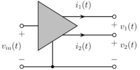
Fig. 1. Typical structure of a differential driver with its relevant port variables. Our proposed modeling framework is based on a generic multiport (differential) driver structure, as depicted in Fig. 1, where the individual single-ended output currents i1,2 and
voltages v1,2 are defined. These are readily converted, if
desired, into differential and common-mode quantities, as vd = v1− v2, vc =
v1+ v2
2 . (1)
Similarly, conversion to single-ended and/or differential scattering representations in terms of incident and reflected transient wave signals can be considered too, leading to a pure scattering formulation as in [22]. In the following, we base our derivations to single-ended voltages and currents for simplicity of illustration, but any other representation that can be linearly related to such variables can be adopted as a starting point as well. Our numerical implementation is based on single-ended scattering variables for improved numerical robustness.
With reference to Fig. 1, we propose the following model structure
i(t) = −Gv(t) + j(t) + g(v(t)) (2) where vectors i = [i1, i2]T and v = [v1, v2]T collect the port
variables. In (2) we recognize various terms as follows:
• the static behavior of the output port currents is captured by a constant conductance matrix G;
• the dynamic behavior of the driver when excited at its output by the voltages v is represented by a dynamical Linear Time-Invariant (LTI) submodel g;
• the time-varying source term j(t) = [j1(t), j2(t)]T
repre-sents the switching activity of the driver as a time-varying analog waveform. This switching activity results from the particular bit pattern imposed by the inner stages of the driver, which are represented in Fig. 1 by the voltage vin(t).
The model structure (2) is indeed a particular case of two well-established formats for behavioral transceiver representa-tion, namel the IBIS standard and the MpiLog framework [4], [6], [8], [17], see also [23]. We recall that basic Mpilog models are written as time-varying combinations of two-piece dynamical submodels as
i(t) = wH(t)FH(v(t)) + wL(t)FL(v(t)) (3)
where Fν with ν ∈ {H, L} are nonlinear dynamical
mul-tivariate relations accounting for the static and the dynamic behavior of the driver in fixed logic states, and wν are
time varying switching functions. A very similar structure holds for IBIS [4], with some simplifications. The proposed model structure (2) can be readily derived from (3) under the following assumptions:
• the two switching functions describing the analog tran-sitions L → H and H → L are constrained to be symmetric through wH(t) = 1−wL(t), which effectively
represents switching behavior through a single time-domain signal;
• the Fν submodels, which can be highly nonlinear and
dynamic in some applications [6], [9], [10], are here approximated by LTI compact models through
Fν(v) = −Gνv + Iν+ gν(v), ν ∈ {H, L} (4)
where the conductance matrices Gν and the static bias
current vectors Iν define linear multivariate static
char-acteristics (in Norton form) approximating the static behavior of the device in each logic state (see Fig. 2 (top panel), which considers the behavior of a commercial 90-nm low-power driver available as a transistor-level encrypted netlist [21]); we denote with gν the two LTI
submodels that reproduce the dynamical response of the device.
Using the two above simplifications in (3) leads to i(t) = wH(t) [−GHv + IH+ gH(v)] +
+(1 − wH(t)) [−GLv + IL+ gL(v)]
(5)
Introducing now the additional assumption that the driver is symmetric in both its static and dynamic parts, the represen-tation in (5) can be recast as in (2), where:
G = GH= GL, g = gH= gL (6)
and
j(t) = [wH(t)IH+ (1 − wH(t))IL] . (7)
Assumption (6) may appear overly restrictive, but extensive numerical tests on various benchmark cases demonstrated that the accuracy loss is negligible when modeling high-speed differential drivers. In particular, this assumption is crucial for ensuring computational efficiency.
III. CONSTRUCTING TRANSCEIVER MODELS Model parameters can be readily obtained via a simple estimation procedure based on a set of Transistor-Level (TL) simulations. Specifically, the 2 × 2 matrix G and the vectors Iν, defining the approximated linear static characteristics are
computed via simple least-squares fits from the real static multivariate surfaces of the device response when operating in a fixed logic state. These responses are extracted by a set of double DC sweeps computed, e.g., in SPICE. The proposed linear approximation corresponds to two planes, depicted for a test driver in Fig. 2 (top panel) in gray solid color. Note that these two planes corresponding to H and L static characteristics are parallel, since we enforce GH = GL = G,
while the DC current offsets IH and IL define the reference
bias levels of each logic state. The figure shows that the approximation of the actual DC characteristics with parallel planes is excellent, as highlighted by the error surfaces shown in the bottom panel of Fig. 2. The error in magnitude turns out to be always less than 0.5 mA in the full considered region of the port voltages v1and v2. In particular, the above mentioned
error is one order of magnitude less (i.e., < 50 µA) in the zone explored during normal operation of the device (see the black stars in the top panel), thus enabling the proposed modeling assumption.
The switching sources j(t) are instead computed from (2) from a set of current and voltage responses of the driver switching on a given load, according to the setup in the top panel of Fig. 3. The device is driven to produce a set of complete transition events, i.e., a “010” bit pattern, allowing to generate the basic switching sources associated to the corresponding up or down transitions. The load is chosen to cancel the effects of the dynamical contribution g. For the i−v representation (2), the above mentioned load corresponds to two ideal short circuits connected between the positive and negative output terminals of the device and ground, forcing v1 = 0 and v2 = 0. For the scattering representation which
is indeed adopted in the present work, two single-ended 50 Ω
resistors are considered instead. The switching term j(t) plays in our framework the same role of the weighting functions wν(t) in standard IBIS/Mpilog models, providing in particular
an effective behavioral representation of the TX-FFE blocks.
0.2 0 -10 -0.2 -5 -0.3 -0.2 0 -0.1 0 0.1 5 0.2 10 0.2 0 -0.2 -1 -0.3 -0.2 -0.1 0 0.1 0.2 -0.5 0 0.5
Fig. 2. Top Panel: trajectory of the current response i1(t) of an example driver
during a real simulation test with a lossy channel (black stars). The trajectory is superimposed to the real and the approximated static characteristics of the driver in the fixed logic H or L states, i.e., isH and isL, respectively (gray
color corresponds to the planes of the linear approximation). Bottom panel: error computed between the actual and the approximated static characteristics at the H (blue surface) and L (red surface) fixed logic state.
For the dynamical submodel g, a multiport state-space structure is assumed, with parameters computed through a Time-Domain Vector Fitting (TDVF) process [20] applied to the transient responses of the currents i1(t) and i2(t) and
voltages v1(t) and v2(t), collected when the driver switches
on a transmission line load (see the testbench shown in the bottom panel of Fig. 3, where the far-end load consists of two resistors connected to an ideal voltage source forcing the nominal common mode voltage VC,nom). We remark that the
TDVF algorithm is able to identify a LTI system from its transient responses excited by arbitrary inputs. This feature is particularly useful here, since both inputs and outputs used for the identification of submodel g are known only implicitly and are obtained by extracting port voltages and currents from the results of a dedicated transient analysis testbench. As an example, Fig. 4 shows the transient voltages and current i1(t)
for the above mentioned test case. Model prediction is included as well, highlighting its good accuracy in reproducing the rich dynamical behavior of the driver.
Fig. 3. Testbenches used for the collection of device responses required for model parameters estimation. Top panel: .TRAN analysis used for the computation of the switching terms j(t) = [j1(t), j2(t)]T; bottom panel:
.TRAN analysis used for the computation of the dynamical submodel g. See text for details.
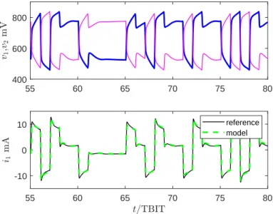
55 60 65 70 75 80 400 600 800 55 60 65 70 75 80 -10 0 10 reference model
Fig. 4. Top panel: example transient responses of the voltages v1(t) and
v2(t) collected when the driver switches on a transmission line load (see
Fig. 3). Bottom panel: dynamical part of the response of the current i1(t) for
the same test case, compared with the response of the dynamical submodel g for the first terminal current. The above waveforms, toghether with the companion response of i2(t) are used for the identification of g.
model is completely linear, thus enabling frequency-domain methods for fast simulation. Differently from the widely-adopted IBIS-AMI standard (which is also based on linearity), the proposed model is better grounded in circuit theory and natively multivariate, thus allowing for an accurate represen-tation of both the differential and the common mode signals.
IV. MODELING LONG-TERM MEMORY EFFECTS OF TX-FFEBLOCKS
We now consider embedding an appropriate representation of FFE blocks in the proposed driver model structure. Es-sentially, TX-FFE circuitry boost the driver strength when
5 10 15 20 25 30 35
-200 0 200
400 without FFEwith FFE
Fig. 5. Switching pattern of the differential voltage vd(t) = v1(t) − v2(t)
with and without FFE for the example driver.
switching occurs, in order to induce a high-pass behavior that should compensate the inevitable low-pass characteristic of the channel due to metal and dielectric losses. Modern CAD tools for channel simulation and eye diagram construction embed effective and simple-to-use FFE blocks, which are commonly represented as Finite-Impulse-Responses (FIR) filters. Given a single-bit pulse p(t) that would be applied without FFE activated, the enhanced pulse with FFE is represented as
˜ p(t) = ¯ r X r=−r αrp(t − rTB), (8)
where TB is the bit time, αr are suitable weights used to
design the FIR frequency response, and r, ¯r denote the number of precursors and postcursors, expressed as translated and rescaled identical replicas of the main pulse p(t). When the boosted elementary pulse ˜p(t) is used for transmitting a given bit pattern {Bk ∈ {0, 1}, k = 1, 2, . . . }, the resulting analog
waveform is still expressed as a superposition of identical replicas of the initial pulse p(t),
X k Bkp(t − kT˜ B) = X k ¯ r X r=−r Bkαrp(t − (r + k)TB) (9)
as a consequence of the assumed translation invariance. Evidence collected from several numerical experiments challenges the above representation of the pre-emhpasis be-havior. Let us consider Fig. 5, where the switching patterns of the example driver is depicted with and without its (1-tap) FFE activated. The analog waveform without FFE is well-described by a superposition of switching events with the same analog rising and falling fronts and can thus be represented as a weighted superposition of successive translations of a single and well-define pulse shape p(t). Conversely, when FFE is enabled, we observe that the expected boosting effect is characterized by some slow transients: the maximum peak-to-peak amplitude of the waveforms is obtained after a few successive switchings, with a slow dynamic saturation effect. This effect makes each individual switching front different from each other, based on the number of earlier consecutive switching events. This effects has a well-defined extent in time, which can be estimated in Fig. 5 to last for about 4– 5 bit times TB for this particular device. We conclude that
a linear FIR approximation as in (8) is not adequate for this driver, since the shape of the switching fronts is not translation-invariant. What is instead required is a nonlinear description of the TX-FFE block, which is able to reproduce the switching front dependence on the number of immediately preceding consecutive switchings.
A. Hierarchical functions for FFE representation
The non-linear and adaptive representation of analog switch-ing fronts that depend on the particular bit pattern is here obtained by a simple constructive approximation process. The main idea shares a common background with widely adopted adaptive approximation framework as those enabled by wavelet decompositions or image and video compression. An initial coarse-level approximation is derived, which pro-vides a gross approximation of the response. Successive details are then added where a correction is required, in order to refine approximation. Corrections are added hierarchically through levels, until a sufficiently small approximation error is attained. The main enabling factor for proposed approach is the finite memory length in time of the TX-FFE analog behavior (see Fig. 5), which in turn induces sparsity, so that corrections need to be applied only locally and with a sparsity pattern that increases with increasing hierarchical levels.
Let us consider each of the two driver source components (n = 1, 2) in (7), which we detrend from their initial condition as ξn(t) = jn(t) − jn(0), and which we represent through the
following sparse hierarchical superposition
ξn(t) = L X `=0 h X k∈Ω(`)n,u ϕ(`)n,u(t − kTB) + X k∈Ω(`)n,d ϕ(`)n,d(t − kTB) i . (10) The signal ξn(t) is expressed as a superposition of individual
L → H and H → L transitions, denoted respectively with the subscripts u, d. In (10), the index ` ranges through hierarchical approximation levels, up to a maximum level L. The construction of these levels is discussed below.
Let us first assume that no FFE is applied, so that no successive approximations are required. In such case, we set L = 0 (index ` is removed). The signal ξn(t) is thus
constructed as a sequence of individual transitions L → H and H → L, centered respectively at time instants k ∈ Ω(0)n,u and
k ∈ Ω(0)n,d. The rising and falling fronts are represented through dedicated basis functions ϕ(0)n,u(t) and ϕ(0)n,d(t), respectively.
If translation-invariance holds, then these two basis functions are sufficient to reconstruct all switching events. For instance, a single-bit pulse p(t) can be represented with only two switching events as
p(t) = ϕ(0)n,u(t) + ϕ(0)n,d(t − TB) (11)
Consider now the case where FFE is activated, so that the shape of a switching event at t = kTB changes depending
on the presence of another switching event at the immediately preceding time t = (k − 1)TB. We collect in sets k ∈ Ω
(1) n,u
and k ∈ Ω(1)n,d such switching instants. It is clear that
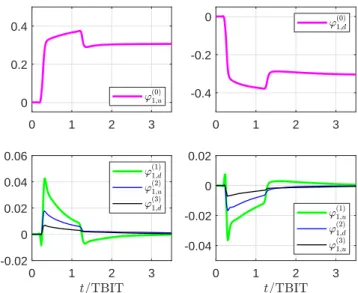
Ω(1)n,ν ⊂ Ω(0)n,ν, ν ∈ {u, d}, (12) 0 1 2 3 0 0.2 0.4 0 1 2 3 -0.4 -0.2 0 0 1 2 3 -0.02 0 0.02 0.04 0.06 0 1 2 3 -0.04 -0.02 0 0.02
Fig. 6. Basis functions ϕ(`)n,u(t) and ϕ (`)
n,d(t), for n = 1 and ` = {0, 1, 2, 3}.
since there are switching events that are preceded by at least two non-switching intervals. We define two level-1 basis functions ϕ(1)n,u(t) and ϕ(1)n,d(t) as the local corrections that need
to be applied to the level-0 approximation, in order to account for the difference in switching waveforms due to the presence of an immediately preceding switching event. We use these basis functions, centered at kTB with k ∈ Ω
(1)
n,u and k ∈ Ω (1) n,d,
respectively, to obtain a refined approximation.
The process is then iterated through levels ` = 2, . . . , L, by identifying the index sets k ∈ Ω(`)n,u and k ∈ Ω(`)n,d
correspond-ing to switchcorrespond-ings that are preceded by at least ` consecutive switchings. Approprate basis functions ϕ(`)n,u(t) and ϕ(`)n,d(t)
are used to represent the correction that is required locally at those instants. As a result, the hierarchical approximation (10) is obtained, where less and less basis functions are needed when the level ` increases, since by construction
Ω(`)n,ν⊂ Ω(`−1)
n,ν , ν ∈ {u, d}, ` = 1, . . . , L. (13)
In addition to sparsity, the signal representation (10) has another very convenient feature. As depicted in Fig. 6, the am-plitude of such basis functions decreases with increasing levels `. This makes the proposed hierarchical representation more and more accurate as the levels increase, in a predictable and controllable manner. It is expected that uniform convergence holds to the exact signals, provided of course that no other sources of errors is present (e.g., the driver behaves exactly as a linear structure, which is not true in general).
As already mentioned, the size of the index sets Ω(`)n,u
and Ω(`)n,d decreases when increasing `, since the probability of occurrence of consecutive ` switching events decreases. These index sets are determined by a digital preprocessing of the logic bit sequence and they are exact, so that the computatioal complexity in the construction of the hierar-chical approximation (10) is known in advance. Therefore, the signal construction is based on a nonlinear and adaptive approximation, which is however based on a sequence of iterative (through levels) linear superpositions of known basis functions.
B. Estimation of hierarchical basis functions
We now consider the construction of the basis functions ϕ(`)n,u(t) and ϕ(`)n,d(t). These are estimated for each level `
through a recursive peeling procedure, starting from a training response pair ˆξ(`)n,u and ˆξn,d(`) computed using the reference TL
driver model excited respectively by a pair of bit sequences Su(`), Sd(`) that include all combinations of required switching
patterns. Estimation is performed via incremental subtraction, while truncating the duration of transient sequences (the basis functions) at a time ¯T`, determined when the expected
steady-state is reached. In particular:
• at level ` = 0, only isolated switching events are used to
define the basis functions as S(0)
u = {0,1,1,1,...}
ϕ(0)n,u(t) = ˆξn,u(0)(t) for the ν = u transition and
Sd(0) = {1,0,0,0,...} ϕ(0)n,d(t) = ˆξn,d(0)(t)
for the ν = d transition.
• at level ` = 1, two consecutive switching events are used to define the basis functions as
S(1)
u = {0,1,0,0,0,...}
ϕ(1)n,u(t) = ˆξn,u(1)(t) − ϕ(0)n,u(t) − ϕ(0)n,d(t − TB)
for the ν = u transition and
Sd(1) = {1,0,1,1,1,...}
ϕ(1)n,d(t) = ˆξn,d(1)(t) − ϕ(0)n,d(t) − ϕ(0)n,u(t − TB)
for the ν = d transition.
• at level ` = 2, three consecutive switching events are
used to define the basis functions as S(2) u = {0,1,0,1,1,1,...} ϕ(2)n,u(t) = ˆξn,u(2)(t) − ϕ(0) n,u(t) − ϕ (0) n,d(t − TB) − ϕ (0) n,u(t − 2TB) − ϕ(1) n,u(t) − ϕ (1) n,d(t − TB)
for the ν = u transition and Sd(2)= {1,0,1,0,0,0,...} ϕ(2)n,d(t) = ˆξn,d(2)(t) − ϕ(0)n,d(t) − ϕ(0)n,u(t − TB) − ϕ (0) n,d(t − 2TB) − ϕ(1)n,d(t) − ϕ(1)n,u(t − TB)
for the ν = d transition.
• at higher levels ` > 2, the process is iterated by consid-ering ` + 1 consecutive switching events and defining the basis functions by removing all contributions required by the approximation of the training signals based on the basis functions at levels up to ` − 1.
A graphical illustration of the estimated basis functions span-ning four levels ` = 0, 1, 2, 3 for the example driver of Fig. 5 is provided in Fig. 6.
V. COMPLETE CHANNEL SIMULATION AND RESULTS Once all basis functions ϕ(`)n,ν(t) are estimated from suitable
identification signals, and the index sets Ω(`)n,ν in the
hierarchi-cal approximation (10) are available for a given bit pattern, the transient switching waveforms j(t) of the driver model (2) are completely determined. The driver model is then completed with the static conductance G and DC biasing terms Iν, as
discussed in Sec. III.
We can now use this model to establish a fast transient simulation framework for a complete high-speed link, includ-ing a complete channel description together with the analog input impedance of the receiver (also assumed to behave as a LTI system) and its Continuous-Time Linear Equalization (CTLE) block, if present. As Fig. 7 shows, the entire system from driver up to the analog receiver part is a LTI system subject to a transient input j(t). Let us then consider the desired output (voltage) waveforms ηm(t) = vm(t) − vm(0),
where also in this case a DC shift by the initial operating point has been applied to setup a transient simulation with zero initial conditions. Due to linearity, the transfer func-tion Hmn(jω) between the n-th input component jn(t) and
the m-th output component ηm(t) can be determined by a
standard frequency-domain analysis, by suitably cascading all frequency-dependent characterizations of the various blocks. This setup is the same as in standard AMI tools.
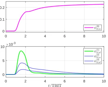
We now exploit the linear superposition in (10). Although this model is obtained as an adaptive nonlinear approximation, the latter is predetermined and statically computed once the bit pattern to be simulated is known. Therefore, we can consider (10) as a superposition of known elementary transient waveforms, one for each of the 2(L + 1) basis functions. A standard Fast Fourier Transform (FFT) processing is then applied to evaluate the response at the output due to a single individual basis function, which is expressed as
ψ(`)mn,ν(t) = F−1nHmn(jω) · F
n
ϕ(`)n,ν(t)oo (14) where F is the discrete Fourier operator (see Fig. 8). Thanks to superposition, the received voltages are then expressed as
ηmn(t) = L X `=0 h X k∈Ω(`)n,u ψ(`)mn,u(t−kTB)+ X k∈Ω(`)n,d ψmn,d(`) (t−kTB) i (15) Note that this expression is identical to (10) but uses different (known and predetermined) basis functions. In particular, it inherits sparsity due to the hierarchical multilevel expansion. The index sets Ω(`)n,ν are unchanged.
The constructive approximation at the receiver is illustrated in Fig. 9. The top panel shows the received voltages at the end of a coupled lossy channel driven by the driver of Fig. 5 with FFE enabled. The different curves demonstrate the increasing approximation quality as the number of levels is augmented. When only level ` = 0 is included, only single and isolated switching events are correctly represented. Including also level ` = 1 provides an accurate representation of any pair of bits that are consecutively switching. Adding more levels leads to convergence for all possible switching sequences.
Fig. 7. Channel response computation. 0 2 4 6 8 10 0 0.1 0.2 0 2 4 6 8 10 0 5 10 10 -3
Fig. 8. Subset of individual basis functions ψmn,u(`) (t) and ψ(`)mn,d(t), for
m = n = 1 and ` = {0, 1, 2, 3} reproducing the received signal at the far end of the channel, obtained by FFT/IFFT processing of the corresponding basis functions ϕ(`)n,u(t) and ϕ(`)n,d(t) depicted in Fig. 6.
We conclude this Section with a few remarks. First, the proposed constructive approximation is able to estimate also common-mode signals in coupled channels, an example will be provided in next section. Second, nothing prevents applica-tion to multiconductor channels with more than two coupled signals, as far as adequate coupled models are available for all system parts. Finally, since the proposed constructive ap-proximation aims at releasing the translation-invariance of the algorithmic TX-FFE part typical of the IBIS-AMI framework, it is expected that with minimal (and possibly no) modifica-tions, the same approach can approximate well the responses of drivers operating in overclocking conditions, where similar effects due to single bit pulse responses extending beyond bit time are observed. A detailed analysis of this scenario is left to a future report. 18 20 22 24 26 28 -500 0 500 18 20 22 24 26 28 200 300 400 500 18 20 22 24 26 28 -100 0 100
Fig. 9. Received voltages computed through superposition of increasing hierarchical levels (top) and error (bottom).
VI. RESULTS
All numerical results presented in this section were obtained using a Workstation equipped with an Intel Core i9-7900X CPU @ 3.30 GHz and 32 GB RAM. For the same example driver considered in the previous sections (henceforth testcase #1) transmitting at a data rate of 3.125 Gbps and a real channel, Figure 10 compares the received differential and common-mode voltages computed using the true TL driver common-model with the results predicted by the proposed approach and the standard IBIS-AMI model. The responses predicted by the proposed linear model in (2) are obtained by post-processing the received waveforms (15), which are conveniently converted into the corresponding transient responses. This comparison highlights the superior accuracy introduced by the proposed approach. The bottom panel of Fig. 10 lacks the prediction for the common-mode voltage from the IBIS-AMI simulation, since this waveform is not supported by the current IBIS-AMI model structure. The common-mode voltage prediction of proposed approach is instead fairly accurate, with an ap-proximation error that is likely due to the residual nonlinearity of the driver, which is here approximated as a pure LTI system. Figure 11 shows the eye diagram (including jitter and crosstalk) obtained for a PRBS-31 pattern of one million bits (this bit stream was selected just to avoid any periodic repetition in the bit pattern). Thanks to linearity, common approaches for inclusion of deterministic and random jitter, as well as crosstalk, can be used in a post-processing phase, as in standard IBIS-AMI flows. Our prototypal non-optimized MATLAB implementation provided this result in 24 seconds. This performance should be compared to a state-of-the-art AMI solver, when applied to the same testcase. The IBIS-AMI was simulated on the same hardware used to run the proposed model. The cumulative runtime was 1.7 seconds for the statistical simulation (which is not comparable in scope with our full transient simulation). Conversely, the bit-by-bit simulation (one million bit-by-bits) with the IBIS-AMI solver required 49 seconds. These times include parsing and all pre-processing steps by the adopted commercial solver. Therefore, we see that the full transient simulation based on the proposed approach is even faster than a high-end commercial software, with the additional advantages of common mode estimation and accurate prediction of non-ideal TX-FFE effects.
In terms of accuracy, both the IBIS-AMI model and the proposed hierarchical solver are seen to underestimate Eye Width (EW) and Height (EH) with respect to the TL results. However, the relative errors of proposed method (10% and 17%, respectively on EW and EH) are significantly smaller than what is achieved by IBIS-AMI (30% and 42%). We remark that these errors are exceedingly large for allowing reli-able use of such models in channel qualification, and should be regarded as a worst-case scenario due to the particularly strong non-ideal TX-FFE behavior of this particular TL device. The above results are thus a clear indication that any model should be used only within its limits of applicability.
As a second validation, Fig. 12 and Fig. 13 collect similar comparisons for a more recent commercial 40-nm low-power driver [21] transmitting at a data rate of 2.5 Gbps, denoted as
50 55 60 65 70 75 80 85 -200 -100 0 100 200 50 55 60 65 70 75 80 85 640 650 660
Fig. 10. Test case #1. Received differential (top) and common-mode (bottom) voltages, computed by different models.
-1 -0.5 0 0.5 1 UI -200 -100 0 100 200 mV
Fig. 11. Test case #1. Eye pattern obtained by processing a 106 bit stream.
testcase #2. Both figures report a comparison of the proposed approach with a reference TL simulation and with a prediction achieved by a nonlinear Mpilog macromodel [6]. This second test further confirms the excellent accuracy of the proposed approach in reproducing the rich dynamical behavior of the device. Concerning the simulation times, the TL simulation takes 1146 seconds to simulate 4500 bits, the Mpilog model takes 739 seconds, whereas the same simulation based on the proposed hierarchical linear model requires less than 1 second. For this driver, the eye pattern shown in Fig. 13 exhibits a wider opening and reduced dynamical effects with respect to the one obtained for the previous and older device (see Fig. 11). Similar to the previous testcase, the CPU-time required for the eye diagram construction with one million bits is about 27 seconds with proposed method, and about 50 seconds with the IBIS-AMI bit-by-bit solver. In terms of accuracy, the proposed solver allows estimating the EW and EH with a relative error of 6% and 8%, respectively, which is comparable to the accuracy achieved by the IBIS-AMI model (i.e., 5% and 9%) and it is exactly the same of the one provided by the Mpilog model (i.e., 6% and 8%). Thus, we see that all models are nearly equivalent in the estimation
Fig. 12. Test case #2. Received differential voltages (top), computed by a reference transistor-level model, the proposed hierarchical simulator, an Mpilog [6] model and by IBIS-AMI. Bottom panel reports the transient error waveforms of the two macromodel-based simulations with respect to the TL reference signals. -1 -0.5 0 0.5 1 UI -200 -100 0 100 200 mV
Fig. 13. Test case #2. Eye pattern obtained by processing a 106bit stream.
of eye diagram metrics, although Fig. 12 clearly illustrates that, for the displayed bit sequence, the IBIS-AMI waveforms appear less accurate than those obtained by Mpilog and by proposed hierarchical solver.
Summarizing, the proposed hierarchical linear model struc-ture performs in all cases with a similar accuracy as the fully nonlinear Mpilog model but requiring simulation times that are comparable to the IBIS-AMI framework, albeit with some small overhead due to the implementation of the constructive hierarchical superposition.
VII. CONCLUSIONS
This paper presented an improved modeling and simulation methodology for the fast simulation of high-speed transmis-sion over differential channels. On one hand, the state-of-the-art and de facto industrial standard IBIS-AMI is extended by proposing a compact linear macromodel of a differential driver which embeds the TX-FFE mechanism via an ad hoc hierarchical-based expansion of its source terms. The proposed model allows the accurate modeling of both the differential and
common mode device responses and a tunable accuracy which depends on the number of basis functions accounted for. On the other hand, channel simulation is done in a mixed time and frequency domain, yielding reduced simulation times and allowing to compute eye patterns for millions of bits in few seconds. This is accomplished net of any code optimization, using a simple prototypal MATLAB implementation.
REFERENCES
[1] M. Swaminathan, C. Daehyun, S. Grivet-Talocia, K. Bharath, V. Laddha, X. Jianyong, “Designing and Modeling for Power Integrity”, IEEE Trans. Electromagnetic Compatibility, Vol. 52, pp. 288–310, 2010. [2] J. Fan, X. Ye, J. Kim, B. Archambeault, A. Orlandi, “Signal integrity
Design for High-Speed Digital Circuits: Progress and Directions,” IEEE Trans. Electromagnetic Compatibility, Vol. 52, No. 2, pp. 392–400, May 2010.
[3] M. S. Sharawi, D. N. Aloi, “Circuit Modeling in High-Speed Designs”, IEEE Potentials, Vol. 24, No. 1, pp. 17–20, 2005.
[4] I/O Buffer Information Specification version 5.1, [Online] Available: http://ibis.org/specs/.
[5] I. S. Stievano, I. A. Maio, F. G. Canavero, C. Siviero, “Reliable eye-diagram analysis of data links via device macromodels”, IEEE Trans. Advanced Packaging, Vol. 29, No. 1, pp. 31–38, Feb. 2006.
[6] I. S. Stievano, I. A. Maio, F. G. Canavero, “Mπlog, macromodeling via parametric identification of logic gates,” IEEE Trans. Advanced Packaging, vol. 27, no. 1, pp. 15–23, Feb. 2004.
[7] I. S. Stievano, I. A. Maio, “Behavioral models of digital IC ports from measured transient waveforms”, Proc. IEEE Topical Meeting on Electrical Performance of Electronic Packaging, EPEP, Scottsdale, AZ, pp. 211–214, Oct. 23–25, 2000.
[8] G. Signorini, C. Siviero, M. Telescu, I.S. Stievano, “Present and Future of I/O-Buffer Behavioral Macromodels”, IEEE Electromagnetic Com-patibility Magazine, Vol. 5, No. 3, pp. 79–85, 2016.
[9] B. Mutnury, M. Swaminathan, J. P. Libous, “Macromodeling of nonlin-ear digital I/O drivers,” IEEE Trans. on Adv. Packag., Vol. 29, No. 1, pp. 102–113, Feb. 2006.
[10] Y. Cao, Q.-J. Zhang, “A New Training Approach for Robust Recur-rent Neural-Network Modeling of Nonlinear Circuits”, IEEE Trans. Microwave Theory and Techniques, Vol. 57, No. 6, pp. 1539–1553, June 2009.
[11] A. K. Varma, M. Steer, P. D. Franzon, “Improving Behavioral IO Buffer Modeling Based on IBIS”, IEEE Trans. Advanced Packaging, Vol. 31, No. 4, Nov. 2008.
[12] W. Dghais, T. R. Cunha, J. C. Pedro, “Reduced-Order Parametric Behavioral Model for Digital Buffers/Drivers With Physical Support”, IEEE Trans. Compon., Packag. Manuf. Technol., Vol. 12, No. 12, Dec. 2012.
[13] T. Zhu, M. B. Steer, P. D. Franzon, “Accurate and Scalable IO Buffer Macromodel Based on Surrogate Modeling”, IEEE Trans. Components, Packaging and Manufacturing Technology, Vol. 1, No. 8, pp. 1240–1249, 2011.
[14] W. Dghais, T. R. Cunha, J. C. Pedro, “A Novel Two-Port Behavioral Model for I/O Buffer Overclocking Simulation”, IEEE Trans. Compo-nents, Packaging and Manufacturing Technology, Vol. 3, No. 10, October 2013.
[15] T. R. Cunha, H. M. Teixeira, J. C. Pedro, I. S. Stievano, L. Rigazio, F. G. Canavero, A. Girardi, R. Izzi, F. Vitale, “Validation by Measure-ments of an IC Modeling Approach for SiP Applications”, IEEE Trans. Components, Packaging and Manufacturing Technology, Vol. 1, No. 8, pp. 1214–1225, 2011.
[16] W. Dghais, J. Rodriguez, ‘’New Multiport I/O Model for Power-Aware Signal Integrity Analysis”, IEEE Trans. Components, Packaging and Manufacturing Technology, Vol. 6, No. 3, pp. 447–454, Mar. 2016. [17] G. Signorini, C. Siviero, S. Grivet Talocia, I.S. Stievano,
“Macro-modeling of I/O Buffers via Compressed Tensor Representations and Rational Approximations”, IEEE Trans. Components, Packaging and Manufacturing Technology, Vol. 6, No. 10, pp. 1522–1534, Oct. 2016. [18] W. Dghais ; M. Souilem ; M. Alam , “Mixed-Signal Overclocked
I/O Buffers Model Abstraction for Signal Integrity Assessment”, IEEE Transactions on Very Large Scale Integration (VLSI) Systems, Vol. 27, No. 3, pp. 691–699, Mar 2019.
[19] C. Siviero, I. S. Stievano, S. Grivet-Talocia, G. Signorini, M. Telescu, “A Fast Channel Simulation Framework Based on Hierarchical Waveform Representations”, Proc. of 2018 IEEE 27th Conference on Electrical Performance of Electronic Packaging and Systems (EPEPS), San Jose (CA), USA, pp. 141–143, Oct. 14–17, 2018.
[20] S. Grivet-Talocia, “Package Macromodeling via Time-Domain Vector Fitting”, IEEE Microw. and Wireless Comp. Lett., Vol. 13, No. 11, pp. 472–474, Nov. 2003.
[21] Official Intel website with products details (https://www.intel.com/-content/www/us/en/products/programmable/stratix-series.html). [22] S. B. Olivadese, S. Grivet-Talocia, C. Siviero, D. Kaller,
“Macromodel-Based Iterative Solvers for Simulation of High-Speed Links With Nonlinear Terminations,” IEEE Trans. Components, Packaging and Manufacturing Technology, vol. 4, no. 11, pp. 1847–1861, Nov. 2014. [23] C. Diouf, Mihai Telescu, I. S. Stievano, N. Tanguy, F. Canavero.
“Simplified topology for IC buffer behavioural models.” IET Circuits, Devices & Systems, 2017, 11 (2), pp. 183–187.
Claudio Siviero received the Diploma degree in electrical engineering and the Ph.D. degree from the Politecnico di Torino, Turin, Italy, in 2003 and 2007, respectively. He was an Electronic Packaging Engineer with IBM Development, Boeblingen, Ger-many, from 2008 to 2013. He is currently a Research Assistant with the Electromagnetic Compatibility Group, Politecnico di Torino, where he works on algorithm development for optimization and order reduction of large-scale dynamical systems, and be-havioral modeling of nonlinear circuit elements, with a specific application to the characterization of digital integrated circuits. His current research interests include macromodeling of electrical interconnects for electromagnetic compatibility and signal integrity problems.
Riccardo Trinchero (M’16) received the M.Sc. and the Ph.D. degrees in Electronics and Communica-tion Engineering from Politecnico di Torino, Torino, Italy, in 2011 and 2015, respectively. He is cur-rently a Researcher within the EMC Group with the Department of Electronics and Telecommunications at the Politecnico di Torino. His research interests include the analysis of linear time-varying systems, modeling and simulation of switching converters and statistical simulation of circuits and systems.
Stefano Grivet-Talocia (M’98–SM’07–F’18) received the Laurea and Ph.D. degrees in electronic engineering from the Politecnico di Torino, Turin, Italy.
From 1994 to 1996, he was with the NASA/Goddard Space Flight Center, Green-belt, MD, USA. He is currently a Full Professor of electrical engineering with the Politecnico di Torino. He co-founded the academic spinoff company IdemWorks in 2007, serving as the President until its acquisition by CST in 2016. He has authored over 150 journal and conference papers. His current research interests include passive macromodeling of lumped and distributed interconnect structures, model-order reduction, modeling and simulation of fields, circuits, and their interaction, wavelets, time-frequency transforms, and their applications.
Dr. Grivet-Talocia was a co-recipient of the 2007 Best Paper Award of the IEEE TRANSACTIONS ONADVANCEDPACKAGING. He received the IBM Shared University Research Award in 2007, 2008, and 2009. He was an Associate Editor of the IEEE TRANSACTIONSONELECTROMAGNETIC
COMPATIBILITYfrom 1999 to 2001 and He is currently serving as Associate
Editor for the IEEE TRANSACTIONSONCOMPONENTS, PACKAGING AND
MANUFACTURING TECHNOLOGY. He was the General Chair of the 20th
and 21st IEEE Workshops on Signal and Power Integrity (SPI2016 and SPI2017).
Igor S. Stievano (M’98–SM’08) received the Master Degree (1996) in Electronic Engineering and the Ph.D. Degree (2001) in Electronics and Commu-nication Engineering from Politecnico di Torino, Torino, Italy. Currently, he is a Professor of Elec-trical Engineering in the Department of Electronics and Telecommunications, Politecnico di Torino. He is the author or coauthor of more than 130 papers published in international journals and conference proceedings. His research interests are in the field of electromagnetic compatibility and signal integrity, with emphasis on modeling and simulation of digital circuits, transmission lines, PLC channels, switching converters and the development of stochastic methods for the statistical simulation of circuits and systems. Recent activities include the compact modeling of electrical and gas networks via a complex network paradigm and simplified graph-based approaches. He was the pro-gram Co-Chair of the 20th and 21st IEEE Workshops on Signal and Power Integrity (SPI2016 and SPI2017). Since 2017 he has been the Vice Rector on academic and scientific activities of the joint campus of Politecnico di Torino in Uzbekistan, “Turin Polytechnic University in Tashkent (TTPU)”.
Gianni Signorini is a Staff Engineer in the “Chip-Package-Board” team of Intel Communication and Devices Group (iCDG). He is leading the execu-tion and methodology development for Signal and Power Integrity simulations of Intel Mobile Modem solutions. Gianni received his B.Sc. (2010), M.S c. (2012) and Ph.D. (2016) in Electronic Engineering from the University of Pisa, Italy. He joined Intel in 2011 and he is based in Munich, Germany.
Mihai Telescu obtained his Engineer’s Degree in Electronics and Telecommunications from the Poly-technic University of Timisoara in 2003. He obtained a Master of Science degree in France in 2004, jointly delivered by the ENSSAT of Lannion and the University of Brest. He received a Doctorate in Elec-tronics from the University of Brest, France in 2007. He was a post doc researcher with the EMC Group at the Politecnico di Torino, Italy between 2008 and 2009. Since 2009 he is an Associate Professor with the UBO. His research interests include linear and non-linear macromodeling, model order reduction, system identification, CAD and related topics. Since 2015 he is also conducting research in signal processing with a focus on digital predistortion.


![Fig. 12. Test case #2. Received differential voltages (top), computed by a reference transistor-level model, the proposed hierarchical simulator, an Mpilog [6] model and by IBIS-AMI](https://thumb-eu.123doks.com/thumbv2/123doknet/11513382.294304/10.918.78.450.84.373/received-differential-voltages-computed-reference-transistor-hierarchical-simulator.webp)
