HAL Id: hal-00604845
https://hal.archives-ouvertes.fr/hal-00604845
Submitted on 28 Nov 2016
HAL is a multi-disciplinary open access
archive for the deposit and dissemination of
sci-entific research documents, whether they are
pub-lished or not. The documents may come from
teaching and research institutions in France or
abroad, or from public or private research centers.
L’archive ouverte pluridisciplinaire HAL, est
destinée au dépôt et à la diffusion de documents
scientifiques de niveau recherche, publiés ou non,
émanant des établissements d’enseignement et de
recherche français ou étrangers, des laboratoires
publics ou privés.
30-band k.p method for quantum semiconductor
heterostructures
Soline Richard, Faycal Raouafi, Alexandre Bondi, Laurent Pedesseau,
Claudine Katan, Jean-Marc Jancu, Jacky Even
To cite this version:
Soline Richard, Faycal Raouafi, Alexandre Bondi, Laurent Pedesseau, Claudine Katan, et al.. 30-band
k.p method for quantum semiconductor heterostructures. Applied Physics Letters, American Institute
of Physics, 2011, 98, pp.251913. �10.1063/1.3600643�. �hal-00604845�
30-band k · p method for quantum semiconductor heterostructures
S. Boyer-Richard,1F. Raouafi,2A. Bondi,1L. Pédesseau,1C. Katan,1J.-M. Jancu,1and J. Even1,a兲1
Université Européenne de Bretagne, INSA, FOTON, UMR 6082, 35708 Rennes, France
2
Laboratoire de Physico-chimie des Matériaux Polymères, Institut Préparatoire aux Etudes Scientifiques et Techniques, BP51, 2070 La Marsa, Tunisia
共Received 28 December 2010; accepted 19 May 2011; published online 23 June 2011兲
We illustrate how the linear combination of zone center bulk bands combined with the full-zone
k · p method can be used to accurately compute the electronic states in semiconductor
nanostructures. To this end we consider a recently developed 30-band model which carefully reproduces atomistic calculations and experimental results of bulk semiconductors. The present approach is particularly suited both for short-period superlattices and large nanostructures where a three-dimensional electronic structure is required. This is illustrated by investigating ultrathin GaAs/ AlAs superlattices. © 2011 American Institute of Physics.关doi:10.1063/1.3600643兴
As high-performance computers are becoming more af-fordable, atomic-scale modeling is gaining importance as an investigative tool in materials science. Complementary ab
initio and empirical approaches within atomic-scale
simula-tions provide detailed information about the physical proper-ties of materials. While first principles techniques, such as density functional theory, are well suited to predict structural and electronic properties over a large energetic region, the calculation of the excited-state manifold of semiconductors is still unsatisfactory.1 In addition, they remain limited to small supercells because of computational cost. The empiri-cal pseudopotential method 共EPM兲 was successfully em-ployed to describe the electronic properties of long period semiconductor superlattices2 共SLs兲. This work was later extended to strained nanostructures using the linear combi-nation of bulk bands 共LCBB兲 共Ref.3兲 approach. LCBB has
demonstrated to be efficient in the calculation of the electron and hole single particle eigenstates of semiconduc-tor quantum dots.4Indeed, full zone Bloch functions form a complete orthonormal set of functions 共COSFs兲. A precise band-structure description can also be obtained for hetero-structures, with a unique submillielectron volt precision throughout the Brillouin zone 共BZ兲, using a spdsⴱ nearest-neighbor tight-binding 共TB兲 model including spin–orbit coupling.5–8 In that case accurate parameters have been op-timized for bulk materials to achieve improved agreement with experiment.9
On the other hand, the need for simple and nonatomistic methods has led to the development of the k · p method and the envelope function approximation共EFA兲.10The k · p/EFA is often used to accurately interpret the excited-state proper-ties of semiconductor SLs and nanostructures but it suffers from several drawbacks such as the description of interface band mixing that exists even for media with no difference in Bloch functions.11 In the EFA, the nanostructure electronic
wave functions are in fact implicitly developed on linear combination of Luttinger–Kohn 共LCLK兲 functions which also form a COSF.12 While a meaningful description of the optical properties of many bulk semiconductors can be ob-tained within the eight-band Kane model near the BZ center,3 at least 30 bands are required for X and L points.4 An improved derivation of the k · p/EFA was proposed later,13 using explicit expansions o the heterostructure wave func-tions on LCLK. This complex k · p/LCLK theory has been rarely used, except to propose a new ordering of differential operators in the k · p/EFA.14 A second example is the pseudopotential-derived multiband k · p method, without spin–orbit coupling, which was proposed for large systems 共⬎10 000 atoms兲 and tested on GaAs/AlAs SLs by Wang and Zunger.15They demonstrated that LCBB and the LCLK are equivalent, provided that unitary transformations exist between the zone center bulk states of various semiconduc-tors forming the heterostructure. It was also shown that a minimum set of 15 basis functions are required to obtain a correct description of the electronic states of bulk materials and the GaAs/AlAs SLs along the ⌫-X line.
In this letter, we propose an alternative to the pseudopotential-derived multiband k · p/LCLK approach15 by starting from a fully empirical 30-band k · p bulk model.16–18 This allows an empirical modeling of bulk ex-perimental band parameters and simple inclusion of spin– orbit coupling. First, we present our 30-band k · p model for bulk semiconductors and the k · p/LCLK method. As an il-lustration, we perform band-structure calculations of ul-trashort period AlAs/GaAs关001兴 SLs.
The k · p method is usually used as a perturbation method to describe the band structure near a given k point of the BZ. It may also work over the full BZ if a large basis set of Bloch states is taken into account, as demonstrated in the
a兲Author to whom correspondence should be addressed. Electronic mail: [email protected].
TABLE I. Dipole matrix elements of AlAs in definition of Ref.16. Energies EPj共⬘兲and matrix elements PPj共⬘兲are linked by EPj共⬘兲= 2m0/ប2关Pj 共⬘兲兴2.
AlAs EP EPX EPd EPXd Ep3 EP3d EP2 EP2d EPS EPU EP⬘
eV 19.14 14.29 0.01 8.49 3.99 9.29 0.032 15.01 1.79 16.00 0.140
APPLIED PHYSICS LETTERS 98, 251913共2011兲
0003-6951/2011/98共25兲/251913/3/$30.00 98, 251913-1 © 2011 American Institute of Physics
seminal work of Cardona and Pollak.18 They used a 15 ⫻15 k·p Hamiltonian without the spin–orbit interaction and obtained a correct description of the valleys of the lowest lying conduction band and valence bands in bulk Si and Ge. However, many new generation device concepts rely on the spin-related properties of semiconductor nanostructures19so that relativist corrections to the band structure have to be considered. The 30-band k · p method is an extension of Car-dona and Pollak’s work with the inclusion of the spin–orbit interaction and a direct fit of the Hamiltonian matrix ele-ments from the experimental band parameters. The quantities included in the fitting procedure are the effective masses and the valence and conduction band energies at⌫, X, and L. It was shown to be valid for Si and Ge in describing the bulk energy states up to 5 eV above the valence band maximum on the first BZ.16 This leads to an accuracy comparable to calculations with the spds* TB models.9 For diamondlike crystals, the 30⫻30 k·p Hamiltonian is completely deter-mined by ten independent parameters and this number grows to eighteen for zinc-blende compounds because of the lack of inversion symmetry. The model parameters can be reduced to eleven for III–V semiconductors without worsening the fit of band structures.16 The parameter values for AlAs are given in TableIand their definitions can be found in Ref.16. Figure1shows the corresponding band structure. Results are found to be in good agreement with the TB calculations all around the BZ and the calculated conduction band minimum 共CBM兲 agrees with the experimental value.20
In addition, the reduced masses and Luttinger parameters compare well with the experimental20 and TB results as seen in Table II. The crucial point of the 30⫻30 k·p method is the continuity
between U关1,1/4,1/4兴 and K 关0,3/4,3/4兴, equivalent points of the BZ which is not obtained by construction in contrast with atomistic approaches as pseudopotential or TB schemes. This discrepancy, observed in an earlier 30-band k · p parametri-zation of AlAs 共Ref. 21兲 is corrected in the present work
except for the second conduction band which is inherent to the formalism.18
The k · p method in EFA is widely used to find the band structure and wave functions of heterostructures.10,22The ba-sic assumption in the EFA approach is the similarity between the matrix elements in the Hamiltonian for most of the semi-conductor compounds near the zone center. Only zone center Bloch functions un,kជ=0共rជ兲 are used in the expansion of the heterostructure wave functions 共n=1–8 in the eight-band
k · p method兲. In the EFA, the un,0共rជ兲 are considered equal in all the materials and it is not necessary to give an explicit expression for them. When considering folded X states in a 关001兴 quantum heterostructure, all these approximations ap-pear to be severe shortcomings.15
In this work, we used a fully empirical 30-band k · p bulk model instead of the pseudopotential-derived multiband k · p Hamiltonian.15 It allows an empirical modeling of bulk ex-perimental band parameters but also the inclusion of spin– orbit coupling in a simple way. Moreover, a new block-diagonalization of the 30⫻30 k·p Hamiltonian into two equivalent 15⫻15 blocks was introduced to calculate the dispersions of the bulk electronic states along the ⌫-X line. Our k · p/LCLK approach is then based on linear com-binations of only 15 LK functions n,kជ共rជ兲=un,0共rជ兲eikជ.rជ, the reduced 15⫻15 blocks of the 30-band k·p Hamiltonian be-ing used to find the matrix elements. Contrary to the pseudopotential-derived multiband k · p model,15 LK func-tions must be obtained independently. In order to keep the model as simple as possible, a basic EPM共Ref.23兲 without
spin–orbit coupling has been used to obtain zone center Bloch functions in each material 共GaAs and AlAs兲. These functions were developed on 15 symmetrized combinations of plane waves.24It preserves unitary transforms between the 15 basis functions of the various bulk materials.15 Clebsch– Gordan coefficients were finally used to yield symmetry-adapted functions fully compatible with the basis of the 30-band k · p bulk model.16 In other words, a precise deter-mination of the eigenenergies is combined with simple but symmetry-adapted expressions of bulk eigenstates wave functions. We may notice that this is the only point at which atomistic information is directly introduced into the calcula-tions. The nanostructure wave functions are expanded on the LK functions of a given material in the heterostructure共e.g., A and B, respectively, for GaAs and AlAs in a GaAs/AlAs SL兲:⌿NS共rជ兲=兺n,kជcn,kជn,kជ
A
共rជ兲. Structure factors are introduced -6 -4 -2 0 2 4 6 AlAs Energy (eV ) L ΓΓΓΓ X U,K ΓΓΓΓ
FIG. 1. Electronic band structure of bulk AlAs calculated with the 30-band
k · p model at T = 0 K. The model parameters are given in TableIand some values of the band energies and effective masses in TableII.
TABLE II. Comparison of the Luttinger parameters, effective masses, and energy levels, obtained in the present work with the 30-band k · p model and compared to the spdsⴱTB calculations and experimental values共Ref.16兲.
␥1 ␥2 ␥3 m共⌫兲 mt共X兲 ml共X兲 mt共L兲 ml共L兲 X6c X7v L6c GaAs共k.p兲 7.18 2.23 2.99 0.067 0.23 1.16 0.11 1.67 1.94 ⫺2.62 1.75 GaAs共TB兲 7.51 2.18 3.16 0.067 0.23 1.24 0.12 1.53 1.99 ⫺3.05 1.85 GaAs共exp兲 6.85 2.1 2.9 0.067 0.23 1.3 0.08 1.9 1.98 ⫺2.80 1.85 AlAs共k·p兲 3.76 0.82 1.42 0.15 0.22 0.97 0.15 1.32 2.26 ⫺2.29 2.48 AlAs共TB兲 3.85 0.69 1.47 0.156 0.23 1.4 0.16 1.37 2.19 ⫺2.51 2.67 AlAs共exp兲 3.69 0.79 1.40 0.146 0.226 1.27 0.14 1.09 2.22 ⫺2.41 2.54 251913-2 Boyer-Richard et al. Appl. Phys. Lett. 98, 251913共2011兲
to take into account unitary transforms between the Bloch functions of bulk materials.15 The resulting k · p/LCLK ap-proach is an improvement over the conventional k · p method in EFA with low computational cost as compared to atomis-tic methods like the EPM associated to LCBB or3,4 extended-basis spdsⴱTB schemes.5–9
We illustrate application of our k · p/LCLK model by considering the case of共GaAs兲n/共AlAs兲nSLs grown lattice-matched on a GaAs substrate. Such heterostructures provide a stringent test for evaluating the performance of ab initio and empirical approaches,2,3,25 as the CBM occurs at a
k-point different from⌫ and depending on the SLs period n.
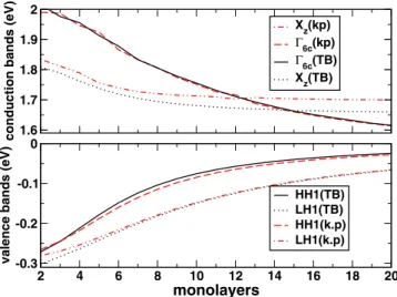
In our calculations, the valence band offset has been chosen in accordance with experimental data: ⌬Ev= 0.55 eV.20,26 Figure 2 compares the k · p and TB near-band-gap energy levels at⌫ of the 共GaAs兲n/共AlAs兲nSLs as a function of the number of monolayers共MLs兲 n.
The two models agree well for the valence and ⌫-like conduction states owing to similarity of the band parameters 共TableII兲. The Xz-levels stem from the bulk AlAs X6c-states folded in the center of the SL BZ. Their variations with
n slightly differ in the two calculations because of difference
in energy position of bulk X6c-states 共Table II兲. In the
30-band k · p model, the quantum size effect associated with the SL period induces a Xz→⌫6c crossover for the critical thickness n = nc⬇13 MLs. It agrees nicely with the experi-mental value at low temperature, nc⬇14,2,3and the present TB result. This corresponds to a significant improvement over pseudopotential-derived multiband k · p calculations3 where nc is found at 7 MLs, as a result of GaAs conduction band mass overestimation. Interestingly, the resulting k · p gap energies become closer to the experimental data for all periods,2 underlying the quality of the present k · p/LCLK approach. For n⬎nc the CBM is a ⌫-like state localized in the GaAs well as evidenced in Fig. 3 for the 共GaAs兲15/共AlAs兲15 SL. Again, we obtain a good agreement between the TB and k · p results for the electron and hole wave functions.
In this work we have proposed a 30-band k · p/LCLK model that allows for simple description of the band diagram
of zinc-blende semiconductors or quantum nanostructures in the whole BZ. It relies on very few adjustable parameters. This is illustrated by modeling the electronic states of the AlAs/GaAs benchmark SLs. Results show a nice agreement with both atomistic calculations and experimental data. Con-trarily to standard k · p/EFA schemes, BZ folding effects are well accounted for. In fact, the Xz→⌫6c crossover is cor-rectly predicted for short-period 共GaAs兲n/共AlAs兲nSLs.
This work was granted access to the HPC resources of CINES under the allocation 2010-关c2010096472兴 made by GENCI共Grand Equipement National de Calcul Intensif兲.
1P. Rinke, A. Qteish, J. Neugebauer, C. Freysoldt, and M. Scheffler,New J.
Phys. 7, 126共2005兲, and references therein.
2D. M. Wood and A. Zunger,Phys. Rev. B 53, 7949共1996兲. 3L. W. Wang and A. Zunger,Phys. Rev. B 59, 15806共1999兲.
4G. Bester, X. Wu, D. Vanderbilt, and A. Zunger, Phys. Rev. Lett. 96,
187602共2006兲.
5J.-M. Jancu, R. Scholz, G. C. La Rocca, E. A. de Andrada e Silva, and P.
Voisin,Phys. Rev. B 70, 121306共2004兲.
6M. Virgilio and G. Grosso,Phys. Rev. B 79, 165310共2009兲.
7N. Kharche, S. Kim, T. B. Boykin, and G. Klimeck,Appl. Phys. Lett. 94,
042101共2009兲.
8F. Sacconi, A. Di Carlo, P. Luigli, M. Städele, and J.-M. Jancu, IEEE
Trans. Electron Devices 51, 741共2004兲.
9J. M. Jancu, R. Scholz, F. Beltram, and F. Bassani,Phys. Rev. B57, 6493
共1998兲.
10G. Bastard and J. A. Brum,IEEE J. Quantum Electron. 22, 1625共1986兲. 11B. A. Foreman,Phys. Rev. Lett. 81, 425共1998兲.
12J. M. Luttinger and W. Kohn,Phys. Rev. 97, 869共1955兲. 13M. G. Burt,J. Phys.: Condens. Matter 4, 6651共1992兲. 14B. A. Foreman,Phys. Rev. B 48, 4964共1993兲.
15L. W. Wang and A. Zunger,Phys. Rev. B 54, 11417共1996兲.
16S. Richard, F. Aniel, and G. Fishman,Phys. Rev. B 70, 235204共2004兲. 17C. R. Pidgeon and R. N. Brown,Phys. Rev. 146, 575共1966兲. 18M. Cardona and F. Pollak,Phys. Rev. 142, 530共1966兲.
19I. Žutić, J. Fabian, and S. Das Sarma,Rev. Mod. Phys. 76, 323共2004兲. 20Semiconductors: Intrinsic Properties of Group IV Elements and III-V, II-VI
and I-VII Compounds, Landolt-Börnstein, New Series, Group III Vol. 22,
Pt. A, edited by O. Madelung共Springer, Berlin, 1987兲.
21N. Fraj, I. Saïdi, S. Ben Radhia, and K. Boujdaria,J. Appl. Phys. 102,
053703共2007兲.
22J. Even, F. Dore, C. Cornet, and L. Pedesseau,Phys. Rev. B 77, 085305
共2008兲.
23J. R. Chelikowsky and M. L. Cohen,Phys. Rev. B 14, 556共1976兲. 24F. Bassani and M. Yoshimine,Phys. Rev. 130, 20共1963兲.
25R. Scholz, J.-M. Jancu, F. Beltram, and F. Bassani,Phys. Status Solidi B 217, 449共2000兲.
26I. Vurgaftman and J. R. Meyer,J. Appl. Phys. 94, 3675共2003兲. 1.6 1.7 1.8 1.9 2 conduction bands (eV ) Xz(kp) Γ6c(kp) Γ6c(TB) Xz(TB) 2 4 6 8 10 12 14 16 18 20 monolayers -0.3 -0.2 -0.1 0 valence bands (eV ) HH1(TB) LH1(TB) HH1(k.p) LH1(k.p)
FIG. 2. 共Color online兲 Comparison of the near-band gap energies of the 共GaAs兲n/共AlAs兲nSL at the zone center of the BZ as function of period n.
Full and dot lines correspond to TB results, while dash and dash-dot lines correspond to k · p results. The energy zero is taken at the bulk GaAs va-lence band maximum.
0 0.3 0.6 0.9 Γ6c(TB) Γ6c(kp) Xz(TB) Xz(kp) 5 15 25 0 0.3 0.6 0.9 HH1(kp) HH1(TB) 5 15 25 LH1(kp) LH1(TB) monolayers GaAs AlAs density (arb. units ) GaAs AlAs
FIG. 3. 共Color online兲 Hole and electron wave functions of the 共GaAs兲15/共AlAs兲15SL obtained with the 30-band k · p共dash lines兲 and TB
共full lines兲 models.
251913-3 Boyer-Richard et al. Appl. Phys. Lett. 98, 251913共2011兲