HAL Id: hal-02553606
https://hal.archives-ouvertes.fr/hal-02553606
Submitted on 24 Apr 2020
HAL is a multi-disciplinary open access
archive for the deposit and dissemination of
sci-entific research documents, whether they are
pub-lished or not. The documents may come from
teaching and research institutions in France or
abroad, or from public or private research centers.
L’archive ouverte pluridisciplinaire HAL, est
destinée au dépôt et à la diffusion de documents
scientifiques de niveau recherche, publiés ou non,
émanant des établissements d’enseignement et de
recherche français ou étrangers, des laboratoires
publics ou privés.
Composition-Dependent Passivation Efficiency at the
CdS/CuIn 1-x Ga x Se 2 Interface
Marco Ballabio, David Fuertes Marron, Nicolas Barreau, Mischa Bonn,
Enrique Cánovas
To cite this version:
Marco Ballabio, David Fuertes Marron, Nicolas Barreau, Mischa Bonn, Enrique Cánovas.
Composition-Dependent Passivation Efficiency at the CdS/CuIn 1-x Ga x Se 2 Interface. Advanced
Materials, Wiley-VCH Verlag, 2020, 32 (9), pp.1907763. �10.1002/adma.201907763�. �hal-02553606�
M. Ballabio, Prof. M. Bonn, Dr. E. Cánovas Max Planck Institute for Polymer Research Ackermannweg 10, 55128 Mainz, Germany E-mail: [email protected] Dr. D. Fuertes Marrón
Instituto de Energía Solar Universidad Politécnica de Madrid ETSI Telecomunicación
Avda. Complutense 30, 28040 Madrid, Spain Dr. N. Barreau
Institut des Matériaux Jean Rouxel (IMN) – UMR6502 Université de Nantes
CNRS
2 rue de la Houssinière, BP 32229, 44322 Nantes Cedex 3, France Dr. E. Cánovas
Instituto Madrileño de Estudios Avanzados en Nanociencia (IMDEA Nanociencia)
Faraday 9, 28049 Madrid, Spain
The ORCID identification number(s) for the author(s) of this article can be found under https://doi.org/10.1002/adma.201907763.
DOI: 10.1002/adma.201907763
are an appealing choice for photovoltaics owing to their high absorption coefficient, as a result of their direct bandgap, enabling low-cost thin-film solar cells. In addition, CIGS absorbers can be grown onto flexible, light, and cheap substrates,[2] and have been
reported to be more stable under prolonged sunlight irradiation when compared with other competing thin-film technologies such as those based on cadmium telluride (CdTe), amorphous silicon (a-Si), and novel perovskites.[3] A potential additional
advan-tage of chalcopyrites is that the bandgap onset of CuIn1-xGaxSe2 quaternary alloys
can be easily tuned by controlling the Ga content from ≈1.0 eV (gallium-free, x = 0, i.e., CuInSe2) to ≈1.7 eV (indium-free, x = 1,
i.e., CuGaSe2). This feature allows for
fine-tuning of the bandgap, which should enable a maximum theoretical photocon-version efficiency of 33.7% at an optimum bandgap of 1.34 eV (given by the Shockley– Queisser limit under an AM1.5 solar spectrum).[4,5] Remarkably,
however, the record ≈23% efficiency of state-of-the-art of ZnO/ CdS/CIGS solar cells employ CIGS absorbers with a bandgap of only ≈1.2 eV (Ga content of x ≈ 0.3),[6,7] i.e., about 0.1 eV below
the theoretical optimum.[8,9] This constraint results from the
experimental observation that CIGS based solar cells employing Ga contents exceeding x = 0.3 undergo a significant reduction in photoconversion efficiency, which is largely driven by an increasing open-circuit-voltage deficit relative to the bandgap.[10]
The underlying reasons behind the experimentally observed output-voltage saturation of CIGS-based devices with a highGa content and its associated efficiency drop have been assigned in literature to different types of mechanisms which can be gener-ally classified into bulk- or interface-limiting factors. Concerning bulk mechanisms, substantial differences in the energetics of point-defect formation of In- and Ga-containing species have been reported, with major penalties predicted for high Ga con-tents, that might lead to limitations on the maximum achievable splitting of quasi-Fermi levels (and the output voltage of the oper-ating cells) and hampering type inversion of naturally occurring p-type material.[11,12] Additionally, bulk Ga-dependent trapping
efficiency of minority carriers has been reported,[13,14] an aspect
that might be contributed by a Ga-dependent diffusion effi-ciency into the bulk of elements like cadmium or sodium,[15,16]
which are well-known grain boundary passivators.[17,18]
Alterna-tively, theoretical works have predicted the promotion of meta-stable light-induced acceptors for high-Ga alloys,[19,20] which are The bandgap of CuIn1-xGaxSe2 (CIGS) chalcopyrite semiconductors can be
tuned between ≈1.0 and ≈1.7 eV for Ga contents ranging between x = 0 and x = 1. While an optimum bandgap of 1.34 eV is desirable for achieving
maximum solar energy conversion in solar cells, state-of-the-art CIGS-based devices experience a drop in efficiency for Ga contents x > 0.3 (i.e., for
band-gaps >1.2 eV), an aspect that is limiting the full potential of these devices. The mechanism underlying the limited performance as a function of CIGS composition has remained elusive: both surface and bulk recombination effects are proposed. Here, the disentanglement between surface and bulk effects in CIGS absorbers as a function of Ga content is achieved by com-paring photogenerated charge carrier dynamics in air/CIGS and surface-pas-sivated ZnO/CdS/CIGS samples. While surface passivation prevents surface recombination of charge carriers for low Ga content (x < 0.3; up to 1.2 eV
bandgap), surface recombination dominates for higher-bandgap materials. The results thus demonstrate that surface, rather than bulk effects, is respon-sible for the drop in efficiency for Ga contents larger than x ≈ 0.3.
Chalcopyrite semiconductors based on copper–indium–gallium– diselenide (CuIn1-xGaxSe2, CIGS) are currently commercially
exploited as light-absorbers in thin-film solar cells.[1] CIGS alloys
© 2020 The Authors. Published by WILEY-VCH Verlag GmbH & Co. KGaA, Weinheim. This is an open access article under the terms of the Creative Commons Attribution License, which permits use, distribution and repro-duction in any medium, provided the original work is properly cited.
www.advmat.de www.advancedsciencenews.com
expected to primarily populate the CIGS absorber close to the CdS junction (i.e., primarily a surface effect). Furthermore, Ga-dependent surface effects have been claimed to be responsible for the voltage deficit in state-of-the-art CdS/CIGS interfaces.[21]
For example, the absence of an inversion layer at the interface between CIGS absorber and CdS buffer layer for bandgaps >1.2 eV,[7] or the transition from a barrier-like to a cliff-like
conduction-band alignment with an increasing Ga content on the absorber side of the interface could explain the poor device performance of wide-gap-based CIGS devices.[22] Discriminating
among these scenarios, therefore, requires disentangling sur-face from bulk effects on the carrier recombination processes in CIGS absorbers with different Ga contents, and their interplay with the CdS buffer layer.
In this work, we employ ultrafast photoconductivity meas-urements with sub-picosecond time resolution to investigate carrier dynamics in air/CIGS and device relevant ZnO/CdS/ CIGS interfaces for a set of CuIn1-xGaxSe2 samples with Ga
contents of x = 0.3, 0.5, and 0.7 (with bandgaps of ≈1.2, ≈1.3, and ≈1.5 eV, respectively). Our results demonstrate that while bulk charge dynamics are barely affected by the Ga content of CIGS alloys, surface recombination is stronger for higher Ga contents; this aspect is true for both air/CIGS and ZnO/CdS/ CIGS interfaces. Notably, we also demonstrate that the CdS sur-face treatment of CIGS absorbers is only effective in inhibiting surface recombination for low-Ga-containing samples, having a negligible effect on samples with larger Ga contents (i.e., with x = 0.5 and 0.7). Finally, we resolve that interfacial recombina-tion at the CdS/CIGS interface increases with photon flux for high-Ga samples, consistent with the formation of metastable acceptors at the interface. Our findings are in line with the observed Ga-dependent efficiency trend in device performance and demonstrate that its origin is linked to surface-, rather than bulk-assisted recombination.
Two-micrometer thick CIGS absorbers were deposited by coevaporation following a so-called isothermal three-stage pro-cess.[23] The Ga content of the layers (x) was tuned by adjusting
Ga/In relative atomic fluxes from one deposition to another. Grown samples are denoted as CuIn0.7Ga0.3Se2, CuIn0.5Ga0.5Se2,
and CuIn0.3Ga0.7Se2; associated with a relative Ga content [Ga]
[Ga] [In] x=
+ equal to 0.3, 0.5, and 0.7, respectively. The CIGS
absorbers were deposited on both fused silica and standard Mo-coated soda-lime-glass substrate; the latter batch was used to fabricate complete solar cells; the solar efficiencies (η) were estimated to be 16.1%, 15.3%, and 11.7% for Ga contents of x = 0.3, 0.5, and 0.7, respectively (see the Supporting Infor-mation). Up to six samples were deposited onto fused 1 mm thick silica substrates; three of them remained uncovered (air/ CIGS samples) and three of them were covered by a 50 nm CdS buffer layer applied by chemical bath deposition and 50 nm ZnO by RF-sputtering from a ceramic target (samples denoted as ZnO/CdS/CIGS).
We performed optical pump–terahertz probe (OPTP) experi-ments on the six samples consisting of air/CIGS and ZnO/ CdS/CIGS structures with three different Ga contents.[24,25] For
materials in which the photoexcited layer (l), chosen to be equal to the light penetration depth, is sufficiently thin compared to the sample thickness, it is possible to obtain the photoconduc-tivity of the samples by deriving the following analytic formula that links the measurable THz differential transmission
ref T T ∆
with the transient photoconductivity (Δσ)[26,27]
1 2 0 ref n n Z l T T σ ∆ = − + ⋅ ⋅ ∆ (1) where n1,2 are respectively the refractive indexes, in the THz
range, of the medium before and after the photoexcited region, and Z0 is the free space impedance. In our experiments, the
pump light penetration depth at 800 nm was inferred to be 177, 220, and 340 nm for CuIn0.7Ga0.3Se2, CuIn0.5Ga0.5Se2, and
CuIn0.3Ga0.7Se2, respectively, based on the data published by
Paulson et al.[28] For all the measurements conducted in this
study, we observe a linear correlation between the photon flux and the maximum transient transmittance, demonstrating that the carrier dynamics are probed in the linear regime, and that the carrier mobility is independent of carrier density. The effi-ciency of photogeneration right after light pump excitation is resolved to be unity for all samples (see Figure S1, Supporting Information).
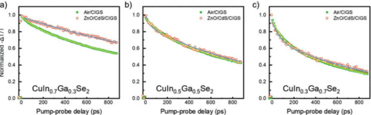
Figure 1 presents three panels comparing normalized TRTS
dynamics for air/CIGS (green traces) and ZnO/CdS/CIGS sam-ples (red traces), as defined by the three analyzed Ga contents. The pump photons (800 nm wavelength and pulse duration
Figure 1. a–c) Normalized optical pump–THz probe dynamics on CIGS samples with Ga contents of x = 0.3 (a), x = 0.5 (b), and x = 0.7 (c). The
green squares represent the decay for the air/CIGS samples, while the red open circles depict the transient signal for the ZnO/CdS/CIGS samples. The solid lines indicate the best biexponential fits to the data (single exponential for the low Ga ZnO/CdS/CuIn0.7Ga0.3Se2 sample). In all cases, the
Figure 1 might—in principle—reveal photoinduced changes in both carrier density and/or mobility as a function of time. Analysis of the THz frequency-resolved complex conductivity (see the Supporting Information) as a function of pump–probe delay demonstrates that mobility is barely affected upon pump– probe delay for each set of samples (i.e., Δµ(t) = µ). As such, the monitored dynamics in each panel of Figure 1 are pri-marily revealing recombination kinetics in the samples (that is, Δσ(t) = eΔN(t)µ). Provided that the electron effective mass is between 2 and 4 times lighter than the hole effective mass for Ga contents between 0 and 1,[29] we interpret our OPTP signal
as describing predominantly electron dynamics.
First, we compare the electron recombination kinetics for samples consisting of air/CuIn1-xGaxSe2 interfaces (green
squares) as a function of Ga content. As evident from the plots in Figure 1, the electron dynamics for air/CIGS samples can be well described by a biexponential function with fast and slow decay time constants of τfast ≈ 100 ps and τslow ≈ 1000 ps
(the origin for this biexponential deactivation path is discussed later). As the Ga content is increased, the overall recombination kinetics becomes faster (see green traces in Figure 1a–c). This result alone demonstrates that increasing Ga contents leads to enhanced recombination rates in the CIGS layers.
Interestingly, comparing air/CIGS kinetics with those obtained from ZnO/CdS/CuIn1-xGaxSe2 samples with high Ga
contents (x = 0.5 and 0.7; red symbols in Figure 1b,c), reveals that charge carrier dynamics are barely affected by the pres-ence of ZnO/CdS overlayers. That is, ZnO/CdS capping does not induce any measurable passivating effect on samples with bandgaps above 1.2 eV. This result demonstrates a negligible effect of the CdS buffer layer on inhibiting surface (or bulk) recombination in samples with a high Ga content. On the other hand, the sample with the lower Ga content (x = 0.3 and bandgap of ≈1.2 eV, the state-of-the-art composition), shows a clear change in recombination kinetics upon CdS treatment. The CdS treatment produces a 24% increase in amplitude at 900 ps after pump excitation that demonstrates unambiguously an improvement in carrier density (photocurrent) resulting from effective passivation of the CdS/CIGS interface. Notably, the CdS capping gives rise to the disappearance of the fast decay component, leaving the dynamics single-exponential, defined only by the ≈1000 ps long-lived τslow component, also
observed for the uncapped samples. Therefore, we can con-clude that the fast component τfast is associated with trapping
at the CdS/CIGS interface (i.e., with interfacial recombination). Overall, the results shown in Figure 1 demonstrate that the passivating effect of the CdS treatment onto CIGS absorbers is
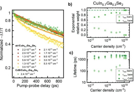
ponent, we performed a fluence-dependent analysis of the samples. The intention was to deliberately saturate surface traps by photodoping. Figure 2a presents optical pump–THz probe traces as a function of incident photon density for the low-Ga sample exposed to air within the range of 3.0 × 10¹²
to 2.2 × 10¹⁴ photons cm-2 per pulse (with estimated carrier
densities in the range between 1.7 × 10¹⁷ and 1.2 × 1019 cm-3,
comparable with solar cell devices operating under 1 sun illu-mination, see the Supporting Information). As it is evident from the plot, increasing the pump fluence for the low-Ga air/ CIGS sample results in a reduction of the weight of the fast recombination component. For sufficiently high photon fluxes, the dynamics become single exponential and defined only by the long-lived ≈1000 ps component. The lifetimes and relative amplitudes obtained from biexponential fits to the data for the evolution of the fast and slow kinetic components as a func-tion of photon flux are summarized in Figure 2b,c. The data reveal that τslow (linked to CIGS bulk recombination) is barely
affected by fluence over the analyzed range of excitations. How-ever, τfast (linked to surface recombination at the air/CIGS
interface) becomes smaller in amplitude and that at elevated photon fluxes, increasingly slower trapping timescales are obtained (consistent with the notion that that trapping rate is directly proportional to trap density).[30–32] Also, we observe that
the carrier dynamics of the low Ga content for ZnO/CdS/CIGS samples at low fluences (open green dots in Figure 2a) corre-late very well with those obtained for air/CIGS samples at high photon fluences, suggesting that photodoping reaches almost the same passivating effect as the CdS-capping. These obser-vations confirm the assignment of the fast and slow trapping components to surface and bulk effects, respectively.
Finally, we performed fluence-dependent analysis for the high-Ga samples (x = 0.5 and x = 0.7 Ga contents, bare data can be found in the Supporting Information). Quantitative analysis of the data, from biexponential fits (see Figure 3a,b), reveal, when compared with the low-Ga sample (Figure 2c), a much weaker trap filling effect (affecting only the fast surface-related component) for the sample with Ga content of x = 0.5. On the other hand, no evidence is found for trap filling in the high-Ga sample (x = 0.7, Figure 3b), which presents almost invariant trapping time constants of ≈100 and ≈1000 ps for all the analyzed photon fluences corresponding to carrier densi-ties ranging from ≈1017 to 1019 cm-3. These results illustrate
that the surface defect population for high-Ga samples is much larger than the maximum carrier density induced by the larger photon flux employed in this study (≈1019 cm-3). The relative
www.advmat.de www.advancedsciencenews.com
Figure 3. a,b) Relative weight of the time constants as a function of the charge carriers photogenerated in the system according to the biexponential
fit for CuIn0.5Ga0.5Se2 (a) and CuIn0.3Ga0.7Se2 (b). c,d) The respective lifetime extracted for the two samples.
Figure 2. a) Comparison between charge dynamics in air/CuIn0.7Ga0.3Se2 with increasing excitation density (solid dots) and CdS/CuIn0.7Ga0.3Se2
high Ga content CIGS absorbers. The Ga content-dependent promotion of interfacial traps induced by light at the CdS/ CIGS surface underlines even more the main conclusion of this paper: Ga-dependent surface recombination—rather than bulk—determines photoconversion efficiency in CIGS samples as a function of Ga content.
In conclusion, we report the interplay between surface recombination and CIGS stoichiometry. We demonstrate that surface recombination is Ga content-dependent for CIGS absorbers, at both air/CIGS and ZnO/CdS/CIGS interfaces; being increasingly dominant for samples with larger Ga con-tents and therefore larger bandgaps. Furthermore, we demon-strate that CdS capping is only effective in removing surface recombination for the low-Ga samples. Our data further reveal the formation of light-induced acceptors at the CdS/CIGS inter-face for high-Ga samples. Altogether, our results correlate well with the observed Ga-dependent efficiency trend in device per-formance and demonstrate that the drop of efficiency in cells made with larger bandgaps can be attributed, at least partially, to surface—rather than bulk—recombination at the CdS/CIGS interface. Note that the relative band alignment at the CdS/ CIGS interface as a function of Ga content might impose as well a Voc deficit in solar cells. Interfacial engineering could,
therefore, prove a way forward for further increasing the effi-ciency of CdS/CIGS-based devices.[33]
Supporting Information
Supporting Information is available from the Wiley Online Library or from the author.
Acknowledgements
D.F.M. acknowledges financial support from Ministerio de Ciencia, Innovación y Universidades, ENE2017-89561-C4-2-R. E.C. acknowledges financial support from the Max Planck Society, the regional government of Comunidad de Madrid (2017-T1/AMB-5207) and the “Severo Ochoa” Programme for Centres of Excellence in R&D (MINECO, Grant No. SEV-2016-0686). The authors acknowledge the collection of preliminary TRTS data on CIGS samples conducted by Dr. Hai Wang and Dr. Soeren Jensen.
Conflict of Interest
The authors declare no conflict of interest.
[2] A. Chirila˘, S. Buecheler, F. Pianezzi, P. Bloesch, C. Gretener, A. R. Uhl, C. Fella, L. Kranz, J. Perrenoud, S. Seyrling, R. Verma, S. Nishiwaki, Y. E. Romanyuk, G. Bilger, A. N. Tiwari, Nat. Mater.
2011, 10, 857.
[3] J. F. Guillemoles, L. Kronik, D. Cahen, U. Rau, A. Jasenek, H. W. Schock, J. Phys. Chem. B 2000, 104, 4849.
[4] W. Shockley, H. J. Queisser, J. Appl. Phys. 1961, 32, 510. [5] S. Rühle, Sol. Energy 2016, 130, 139.
[6] M. A. Green, Y. Hishikawa, E. D. Dunlop, D. H. Levi, J. Hohl-Ebinger, M. Yoshita, A. W. Y. Ho-Baillie, Prog. Photovoltaics Res. Appl. 2019,
27, 3.
[7] R. Herberholz, V. Nadenau, U. Rühle, C. Köble, H. W. Schock, B. Dimmler, Sol. Energy Mater. Sol. Cells 1997, 49, 227.
[8] W. N. Shafarman, R. Klenk, B. E. Mccandless, J. Appl. Phys. 1996,
79, 7324.
[9] A. Yamada, K. Matsubara, K. Sakurai, S. Ishizuka, H. Tampo, P. J. Fons, K. Iwata, S. Niki, Appl. Phys. Lett. 2004, 85, 5607.
[10] P. K. Nayak, S. Mahesh, H. J. Snaith, D. Cahen, Nat. Rev. Mater.
2019, 4, 269.
[11] Y.-J. Zhao, C. Persson, S. Lany, A. Zunger, Appl. Phys. Lett. 2004, 85, 5860.
[12] S. B. Zhang, S.-H. Wei, A. Zunger, H. Katayama-Yoshida, Phys. Rev.
B 1998, 57, 9642.
[13] G. Hanna, A. Jasenek, U. Rau, H. W. Schock, Thin Solid Films 2001,
387, 71.
[14] J. T. Heath, J. D. Cohen, W. N. Shafarman, D. X. Liao, A. A. Rockett,
Appl. Phys. Lett. 2002, 80, 4540.
[15] S. Shirakata, K. Ohkubo, Y. Ishii, T. Nakada, Sol. Energy Mater. Sol.
Cells 2009, 93, 988.
[16] D. Rudmann, G. Bilger, M. Kaelin, F.-J. Haug, H. Zogg, A. N. Tiwari,
Thin Solid Films 2003, 431, 37.
[17] L. Kronik, D. Cahen, H. W. Schock, Adv. Mater. 1998, 10, 31. [18] D. W. Niles, M. Al-Jassim, K. Ramanathan, J. Vac. Sci. Technol., A
1999, 17, 291.
[19] S. Lany, A. Zunger, J. Appl. Phys. 2006, 100, 113725.
[20] J.-F. Guillemoles, L. Kronik, D. Cahen, U. Rau, A. Jasenek, H.-W. Schock, J. Phys. Chem. B 2000, 104, 4849.
[21] T. Minemoto, T. Matsui, H. Takakura, Y. Hamakawa, T. Negami, Y. Hashimoto, T. Uenoyama, M. Kitagawa, Sol. Energy Mater. Sol.
Cells 2001, 67, 83.
[22] R. Klenk, Thin Solid Films 2001, 387, 135.
[23] F. Couzinié-Devy, N. Barreau, J. Kessler, Prog. Photovoltaics Res.
Appl. 2011, 19, 527.
[24] R. Ulbricht, E. Hendry, J. Shan, T. F. Heinz, M. Bonn, Rev. Mod.
Phys. 2011, 83, 543.
[25] H. Neˇmec, P. Kˇuel, V. Sundström, J. Photochem. Photobiol., A 2010,
215, 123.
[26] P. Kužel, F. Kadlec, H. Neˇmec, J. Chem. Phys. 2007, 127, 24506.
[27] P. U. Jepsen, D. G. Cooke, M. Koch, Laser Photonics Rev. 2011, 5, 124.
www.advmat.de www.advancedsciencenews.com
[28] P. D. Paulson, R. W. Birkmire, W. N. Shafarman, J. Appl. Phys. 2003,
94, 879.
[29] R. Chen, C. Persson, Thin Solid Films 2011, 519, 7503.
[30] M. Lambsdorff, J. Kuhl, J. Rosenzweig, A. Axmann, J. Schneider,
Appl. Phys. Lett. 1991, 58, 1881.
[31] H. Wang, I. Barceló, T. Lana-Villarreal, R. Gómez, M. Bonn, E. Cánovas, Nano Lett. 2014, 14, 5780.
[32] F. E. Doany, D. Grischkowsky, C.-C. Chi, Appl. Phys. Lett. 1987, 50, 460.