HAL Id: hal-00822529
https://hal.archives-ouvertes.fr/hal-00822529
Submitted on 1 Jun 2015
HAL is a multi-disciplinary open access
archive for the deposit and dissemination of
sci-entific research documents, whether they are
pub-lished or not. The documents may come from
teaching and research institutions in France or
abroad, or from public or private research centers.
L’archive ouverte pluridisciplinaire HAL, est
destinée au dépôt et à la diffusion de documents
scientifiques de niveau recherche, publiés ou non,
émanant des établissements d’enseignement et de
recherche français ou étrangers, des laboratoires
publics ou privés.
Measurement of the microwave permittivity of polymer
materials for high-speed optical modulator design
Kenny Robert Philippe Auguste, Jean-François Legier, Erick Paleczny,
Mathieu Halbwax, Hind Mahé, Lénaïck Fontanieu, Jean-Pierre Vilcot
To cite this version:
Kenny Robert Philippe Auguste, Jean-François Legier, Erick Paleczny, Mathieu Halbwax, Hind Mahé,
et al.. Measurement of the microwave permittivity of polymer materials for high-speed optical
modula-tor design. 18th Telecommunications Forum (TELFOR 2010), Nov 2010, Belgrade, Serbia. pp.772-774.
�hal-00822529�
Abstract — We report here a technique that we used to
determine the complex permittivity of film structured polymer materials in the microwave frequency range. The goal is to obtain the data that are requested to design the microwave electrodes of Mach-Zehnder type optical modulators. As an example, the technique is applied to two materials that can be used in the fabrication of a high-speed optical polymer based modulator.
Keywords — Mach-Zehnder optical modulator, microwave
permittivity measurement, polymer material, travelling wave design
I. INTRODUCTION
etropolitan access communications systems are currently looking on high data rate capabilities. Moreover, optical networks are and will be undoubtedly used. Depending on requested data rates and data modulation schemes that will be used, high speed optical modulation devices are required for the core access network. Direct modulation of laser diodes is limited to the 10GHz frequency band and external modulation is commonly used for higher modulation frequencies. Lithium niobate (LiNbO3) Mach-Zehnder type modulators
currently offer the requested performance for such
Authors want to acknowledge the financial support of French National Agency for Research under the project "MODPOL".
K. R. Philippe Auguste is with Institut de Recherche en Electrotechnique et Electronique de Nantes Atlantique, Université de Nantes, 2, rue de la Houssinière, BP 92208, 44322 Nantes cedex – France. (email: [email protected]).
Jean-Francois Légier is with Institut d’Electronique, de Microélectronique et de Nanotechnologie, UMR 8520, Université Lille 1, Avenue Poincaré, BP 60069, 59652 Villeneuve d’Ascq cedex – France (email : [email protected]).
Eric Paleczny is with Institut d’Electronique, de Microélectronique et de Nanotechnologie, UMR 8520, Université Lille 1, Avenue Poincaré, BP 60069, 59652 Villeneuve d’Ascq cedex – France (email : [email protected]).
M. Halbwax is with Institut d’Electronique, de Microélectronique et de Nanotechnologie, Avenue Poincaré, BP 60069, 59652 Villeneuve d’Ascq Cedex – France (email : [email protected]).
H. Mahé is with Université Européenne de Bretagne, laboratoire Foton, UMR 6082, CCLO, ENSSAT, BP 80518, 22305 Lannion cedex – France (email: [email protected])
L. Fontanieu is with Université Européenne de Bretagne, laboratoire Foton, UMR 6082, CCLO, ENSSAT, BP 80518, 22305 Lannion cedex – France (email: [email protected])
J-P. Vilcot is with Institut d’Electronique, de Microélectronique et de Nanotechnologie, Avenue Poincaré, BP 60069, 59652 Villeneuve d’Ascq Cedex – France (email : [email protected]).
applications. Nevertheless, since the access points will be numerous, a lower cost technology is sought for. Years ago, polymer materials have been pointed out as, may be, the best challengers to LiNbO3 since they can offer
equivalent even higher performance with a foreseen lower cost technology (see for example [1], [2]).
The design of a Mach-Zehnder modulator requires two main parts. First, the optical waveguide shall be designed following classical rules that are used to design monomode optical waveguides taking into account the refractive index of each layer that composes this optical waveguide, typically the bottom cladding, the core and the top cladding layers. And second, the command electrode shall be designed. Mach-Zehnder modulators are based on a travelling-wave design and in order to get the highest modulation bandwidth, the microwave propagation line shall insure the highest possible match of electrical wave velocity to the optical wave one. This has been a long time taken as the main driving issue for the microwave electrode. Owing to the inherent properties of polymer materials, this is almost easily obtained [1]. Then, it appears that the main bandwidth limiting factor is the value of the propagation losses of this microwave line, taking into account that this later shall also insure impedance matching to the signal generator that is commonly 50 ohms.
Typically, the driving electrode of polymer based modulators is a microstrip line, the substrate of is composed by the optical waveguide (see for example [3]). The perfect knowledge of the polymer material microwave properties, i.e. their permittivity, is so requested in order to design the microstrip line as well as to optimize its performance. Hereby, we report the technique we have developed in order to characterize this permittivity on the frequency range under interest for the devices, i.e. up to 30 GHz.
II. OVERALL TECHNIQUE DESCRIPTION
A. Measurement protocol description
We focus here on dielectric properties measurements, on a wide range of microwave frequencies, rather than the lower one (<1GHz) most commonly studied. To perform as reliable as possible measurements, our protocol follows these steps:
Measurement of the microwave permittivity of
polymer materials for high-speed optical
modulator design
Kenny Robert Philippe Auguste, Jean-Francois Légier, Eric Paleczny, Mathieu Halbwax, Hind Mahé,
Lénaïck Fontanieu, Jean-Pierre Vilcot
1) the study, the design and the technological fabrication of metallic microwave electrodes, i.e. coplanar lines, on a thin polymer film,
2) the measurement of physical parameters, i.e. microwave s-parameters, that can be qualified as starting ones, via the characterization under probes of the metallic electrodes previously fabricated,
3) the extraction of intermediate data, i.e. the complex propagation constant, using a home made de-embedding procedure,
4) finally, a theoretical microwave modelling of the sample using an home made software in order to determine the complex permittivity of the thin film of polymer from the above determined intermediate data.
As it concerns characterization and measurements in the microwave frequency range, the coplanar waveguide structure has been chosen to insure for compatibility with microwave probing stations. At this step, the polymer film of unknown characteristics must be deposited on a reference substrate whose electrical characteristics have to be known either from manufacturer specifications or from own previously made measurements (see below). It is obvious that all the dimensions of the metallic electrodes and dielectric substrate are optimized to avoid spurious microwave behaviours and to insure monomode propagation. Even if the current study is limited at 30 GHz, this method can be applied up to 80 GHz.
Our de-embedding procedure requires different lengths of the same microwave waveguide structure to be measured. The results consist in the scattering matrix of these 2-port components. These measurements are performed with a Cascade Microtech® probe station coupled to an Agilent vector network analyzer.
The final result, i.e. the frequency dependent complex permittivity of the material, is obtained via a home made software. This software must be considered as an expert one; it is especially dedicated to dielectric or magnetic characterization of materials that are structured in thick or thin layers. Based on a vector finite element method, this software gives the complex permittivity or permeability of any layer of finite thickness [4] [5].
B. The practical point of view
The permittivity of the polymer thin film materials are determined from the complex propagation constant knowledge of the coplanar waveguide laid on a double layered structure. This later is made of the polymer to be characterized coated on a semi-insulating GaAs wafer. The polymer thickness is typically a few microns while GaAs substrate is 400 micron thick. A reference sample is constituted by the sole deposition of gold coplanar lines on a GaAs wafer (without any dielectric layer) in order to get the GaAs and metal parameters. The frequency dependence of the propagation constant is extracted from the [S] parameter measurements up to 30 GHz by home made de-embedding software.
From the measurements made on the reference sample, the permittivity and loss tangent of the GaAs material has been determined to be 11.82 and 1x10⁻⁴, respectively. The coplanar electrodes are made of a 0.5 micron thick gold film which conductivity value has been determined close to
33.3 S/µm from the same measurement set. At this stage, all the electrical parameters are set in our dedicated software; when polymer coated samples will be investigated, only the dielectric permittivity of the polymers will be unknown.
Our home made microwave modeling is then used to match the propagation constant extracted from the [S] parameters measurements to the calculated one; the only tuning parameter being the polymer complex permittivity.
C. Characterized materials
In this paper, we will present the results we have obtained on two particular materials that can be used for the fabrication of a polymer modulator but obviously the technique is applicable to any material. The sole limit is linked to the compatibility of the technological process for the coplanar electrode deposition with the tested material. It can be tricky for some polymers. We use the same material as bottom and top cladding: NOA65 material from Norland. This material offers a relatively easiness of technological processing as well as a low resistivity value compared to the one of the active core material [6]; this is beneficial for the chromophore poling process. The core material, APC-CPO1, is made of new chromophore molecules, CPO1, [7] in an amorphous polycarbonate (APC) matrix.
III. RESULTS
The following figures resume the different results we obtained by applying our protocol to the materials that have been previously described. It concerns 5 µm thick NOA65 and 2.5 µm thick APC-CPO1 films deposited on a GaAs substrate whose frequency dielectric characteristics are perfectly known (§II.B). Below we show in graphs the results that have been obtained for the NOA65 material. The same kind of results have been obtained for the active material.
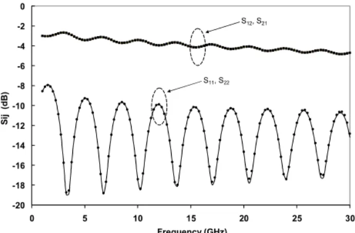
The starting experimental data, the [S] parameters, are shown in Fig. 1, here for the NOA65 sample on the 30 GHz frequency range. -20 -18 -16 -14 -12 -10 -8 -6 -4 -2 0 0 5 10 15 20 25 30 Frequency (GHz) S ij (d B ) S12, S21 S11, S22
Fig. 1. Measured S parameters of a coplanar line deposited on a 5µm thick NOA65 film (the substrate is
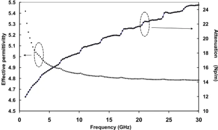
From these data, we extract the intermediate data, the complex propagation constant of the double layered planar guiding structure with the help of the home made de-embedding procedure. This allows determining the effective permittivity of the coplanar propagation line as well as its attenuation (Fig. 2).
4.5 4.6 4.7 4.8 4.9 5 5.1 5.2 5.3 5.4 5.5 0 5 10 15 20 25 30 Frequency (GHz) A tt e n u a tio n ( N p /m ) 10 12 14 16 18 20 22 24 E ff e c ti v e p e rm it ti v it ty
Fig. 2. Effective permittivity and attenuation of the coplanar propagation line fabricated on NOA65 material.
The last step is to extract the complex permittivity, * = ' - j ", from these values using a specifically developed algorithm. The results are shown in Fig. 3 for both NOA65 and APC-CPO1 materials. This allows to get the real part of the permittivity, ', that will be used to design the microstrip line as well as the loss tangent, tg( ) = ''/ ', in order to evaluate the dielectric part of the microstrip line loss value.
1 1.5 2 2.5 3 3.5 4 0 5 10 15 20 25 30 Frequency (GHz) R e la ti v e p e rm it ti v it y 0 0.5 1 1.5 2 2.5 3 3.5 4 4.5 5 tg ( ) ( x 1 0 -2 )
Fig.3. Value of the real part ( ') of the NOA65 ( ) and APC-CPO1 ( ) materials up to 30 GHz. The loss tangent
(tg( )) is also reported for these two materials. IV. DISCUSSION
The mean value of the relative permittivity is 2.85 and 3.2 for APC-CPO1 and NOA65, respectively. The loss tangent value is 8x10⁻³ and 2.2x10⁻² respectively for the same materials. The exact design of the microstrip line, i.e. its width, will strictly depend on the precise geometry of the optical waveguide. Nevertheless, if a mean permittivity value of 3.1 is taken for the NOA65/APC-CPO1 combination, the ratio width/thickness of the microstrip waveguide is close to 2.45. That is to say that, for example,
a 8µm high optical waveguide structure, the width of the microstrip line will be close to 20µm. In other words, whatever the design of the optical waveguide will be, the characteristic impedance of the microstrip line will be 50 1 ohm on the whole potential variation of the effective permittivity value of the materials. Taking into account the loss tangent values that have been extracted, the dielectric part of the microstrip line propagation losses can be assessed in a first approach to be 0.1 to 0.2 dB/cm. In the same approach, the metallic part of these can be evaluated between 1.5 to 2 dB/cm depending on metal thickness.
V. CONCLUSION
We have reported the technique we use to determine the frequency dependent complex permittivity value of polymer materials to be used in optical modulators. As examples, we took the case of NOA65 material and APC-CPO1 materials that act as cladding (passive) and core (active) materials, respectively. The mean value of relative permittivity of those is 3.2 and 2.85, respectively, on the a frequency range up to 30 GHz. The corresponding width/thickness of the microstrip line electrode is then close to 2.5 depending on the optical waveguide conformation (cladding/core structuring). The loss tangent of these materials is around 1x10⁻² and should give dielectric propagation losses of the microstrip line close to 0.2 dB/cm.
REFERENCES
[1] D. Chen, H. R. Fetterman, A. Chen, W. H. Steier, L. R. Dalton, W. Wang, and Y. Shi, “Demonstration of 110 GHz electro-optic polymer modulators,” Appl. Phys. Lett., vol. 70, no. 25, June 1997, pp. 3335-3337
[2] M. Lee, H. E. Katz, C. Erben, D. M. Gill, P. Gopalan, J. D. Heber, and D. J. McGee, “Broadband Modulation of Light by Using an Electro-Optic Polymer,” Science, vol. 298, pp. 1401–1403, Nov. 2002
[3] R. J. Michalak, Y-H. Kuo, F. D. Nash, A. Szep, J. R. Caffey, P. M. Payson, F. Haas, B. F. McKeon, P. R. Cook, G. A. Brost, J. Luo, A. K.-Y. Jen, L. R. Dalton, and W. H. Steier, “High-Speed AJL8/APC Polymer Modulator,” IEEE Photon. Techn. Lett.., vol. 18, no. 11, June 2006, pp. 1207–1209
[4] F. Ponchel, J. Midy, J-F. Legier, C. Soyer., D. Remiens, T. Lasri, and G. Gueguan, “Dielectric microwave characterizations of (Ba,Sr)TiO3 film deposited on high resistivity silicon substrate: analysis by two-dimensional tangential finite element method,”
Journ. Appl. Phys., vol. 107, no.5, March 2010, 054112-1-5
[5] F. Ponchel, J-F. Legier, C. Soyer., D. Remiens, J. Midy, T. Lasri, and G. Gueguan, “Rigorous extraction tunability of Si-integrated Ba0.3Sr0.7TiO3 thin film up to 60 GHz,” Appl. Phys. Lett., vol. 96, no. 25, June 2010, 252906-1-3
[6] S. Michel, J. Zyss, I. Ledoux-Rak, and C.T. Nguyen, “High-performance electro-optic modulators realized with a commercial side-chain DR1-PMMA electro-optic polymer,” at the 2010 SPIE Organic Photonic Materials and Devices XII, conference #7599, San-Francisco, CA.
[7] H. Ibn El Ahrach, A. Barsella, J. Vola, L. Mager, A. F. Fort, W. Bentoumi, Y. Bretonniere, and C. Andraud, “Polarization/depolari-zation processes in NLO side-chain polymers doped with push-pull chromophores,” at the 2010 SPIE Organic Photonic Materials and Devices XII, conference #7599, San-Francisco, CA.