This is an author-deposited version published in :
http://oatao.univ-toulouse.fr/
Eprints ID : 8760
To link to this article : DOI:
10.1088/0957-4484/23/9/095303
URL :
http://dx.doi.org/10.1088/0957-4484/23/9/095303
O
pen
A
rchive
T
OULOUSE
A
rchive
O
uverte (
OATAO
)
OATAO is an open access repository that collects the work of Toulouse researchers and
makes it freely available over the web where possible.
To cite this version :
Seichepine, Florent and Salomon, Sven and Collet, Maéva
and
Guillon, Samuel and Nicu, Liviu and Larrieu, Guilhem
and
Flahaut, Emmanuel and Vieu, Christophe
A combination of
capillary and dielectrophoresis-
driven assembly methods for wafer
scale integration of carbon-nanotube-based nanocarpets
.
(2012)
Nanotechnology, vol. 23 (n° 9). pp. 1
-7. ISSN 0957-4484
Any correspondence concerning this service should be sent to the repository
administrator:
[email protected]
A combination of capillary and
dielectrophoresis-driven assembly
methods for wafer scale integration of
carbon-nanotube-based nanocarpets
Florent Seichepine
1,2,3,4, Sven Salomon
2,4, Ma´eva Collet
2,4,
Samuel Guillon
2,4, Liviu Nicu
2,4, Guilhem Larrieu
2,4,
Emmanuel Flahaut
1,3,4and Christophe Vieu
2,41Universit´e de Toulouse, UPS, INP, Institut Carnot Cirimat, 118 route de Narbonne, F-31062 Toulouse
Cedex 9, France
2Universit´e de Toulouse, UPS, INSA, INP, ISAE, LAAS, F-31059 Toulouse, France 3CNRS, Institut Carnot Cirimat, F-31062 Toulouse, France
4CNRS-LAAS, 7 avenue du Colonel Roche, F-31077 Toulouse, France
Abstract
The wafer scale integration of carbon nanotubes (CNT) remains a challenge for electronic and electromechanical applications. We propose a novel CNT integration process relying on the combination of controlled capillary assembly and buried electrode dielectrophoresis (DEP). This process enables us to monitor the precise spatial localization of a high density of CNTs and their alignment in a pre-defined direction. Large arrays of independent and low resistivity (4.4 × 10⁻⁵ m) interconnections were achieved using this hybrid assembly with
double-walled carbon nanotubes (DWNT). Finally, arrays of suspended individual CNT carpets are realized and we demonstrate their potential use as functional devices by monitoring their resonance frequencies (ranging between 1.7 and 10.5 MHz) using a Fabry–Perot interferometer.
1. Introduction
Carbon nanotubes (CNT) have been studied for nearly two decades as potential new materials for advanced nanoelectronic systems [1]. Metallic CNTs can be used as large current density carriers [2] while semiconducting CNTs are studied for the next generation of field effect transistors [3]. Other applications such as gas sensors, infrared sensors or nanoelectromechanical systems (NEMS) have also been demonstrated [4–8]. Nevertheless, large scale integration of these devices is still undergoing research and efficient processes have to be developed. Patterning precisely CNT catalysts followed by catalytic chemical vapor deposition (CCVD) processes have already been achieved to locally grow vertical CNT forests. The structural quality of the
CNTs can be controlled by engineering the catalyst and optimizing growth conditions [9, 10]. Large scale assembly of complex CNT structures, such as three-dimensional microelectromechanical devices has been reported using localized growth [11].
Yet, to ensure compatibility with complementary metal–oxide–semiconductor (CMOS) fabrication technolo-gies, back-end process temperatures cannot exceed 400–450◦C [12]. These temperatures are not compatible with the usual CNT growth conditions without affecting dramatically their structural quality. On the other hand, ex situ CNTs can be precisely separated according to their size, chirality or electrical properties due to recent advances in CNT selection protocols [13], but novel manipulation techniques are required to integrate ex situ synthesized CNTs
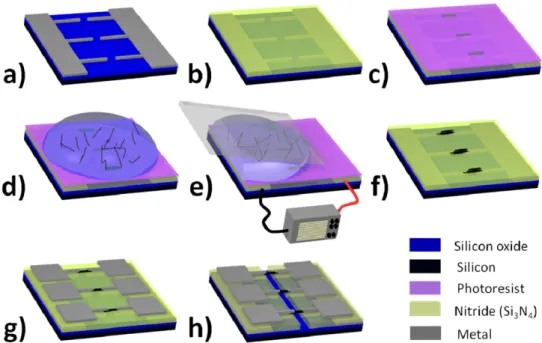
Figure 1. Schematic view of the complete process used to integrate CNTs dispersed in solution by a combination of DEP and capillary assembly. (a) Cr (10 nm)/Au (90 nm) DEP electrodes are patterned on a thermally oxidized (300 nm) silicon wafer. (b) A 300 nm thick silicon nitride (Si3N4) layer is deposited by PECVD on the electrodes. (c) A photoresist is spin-coated on the silicon nitride and cavities are
patterned on the top of the DEP electrodes by proximity UV photolithography. (d) A droplet of homogeneously dispersed CNT suspension is poured on the top of the photoresist. (e) The function generator is used to deliver a localized electric field between the DEP electrodes while the meniscus is scanned at a controlled velocity over the patterns using a capillary assembly system. (f) After assembly the photoresist is removed. (g) The CNT connections are individually connected by Cr (10 nm)/Au (90 nm) independent electrode pairs. (h) The Si3N4
layer can be selectively etched by HF and critical point drying (CPD) for generating CNT suspended nanocarpet arrays.
at the wafer scale [14]. Moreover, due to their specific aspect ratio, CNT properties are highly anisotropic and their orientation should be controlled for most applications where the objective is to take benefit from the intrinsic physical properties of these 1D nano-objects. In this study, we have used DWNT samples which are adapted for application as electrical conductors because 80% of those CNTs possess metallic behavior [15].
Large scale assemblies of oriented CNTs based on the use of capillary forces, mechanical actions or chemical binding have already been reported [16–18]. These techniques are mainly focused on single devices or macroscale integration while assembly processes like the one relying on the use of electrohydrodynamic effects [19] allows both selective deposition and orientation of CNTs. Among those, dielectrophoretic (DEP) forces are induced by nonuniform electric fields and act on polarizable micro- or nanosized objects dispersed in a liquid. When using appropriate solvent and experimental parameters, CNTs can be attracted by the strong electric field gradients [20]. Depending on the electrode configuration, CNTs are either individually connected at large scale, using floating electrode DEP, or high densities of CNTs are connected between DEP electrodes, using conventional DEP [21–23]. It has also been shown that the chirality of the attracted CNTs can be controlled by tuning the DEP parameters [24] and that these processes can be up-scaled for wafer scale implementation [25,26]. Nevertheless, current DEP processes use the DEP electrodes both as assembling and actuating electrodes, which represents a severe limitation for their practical usability. Indeed, a complex interconnection
design between several assembly sites or the independent use of a single device is impossible.
In this paper, we describe a versatile way to integrate dense layers of oriented DWNTs, at the wafer scale, using buried electrode dielectrophoresis coupled to capillary assembly. The DWNTs are oriented along the electric field lines and assembled at pre-defined positions with an adjustable density by controlling independently the capillary and DEP forces. During the whole process, DWNTs are electrically insulated from the DEP electrodes. DWNT assembly sites are then connected individually using a dedicated metallization step whose design is totally unconstrained. Using this original methodology, we demonstrate wafer scale integration of oriented DWNTs into various kinds of elementary devices. By implementing a last etching process step, we demonstrate a proof of concept of suspended CNT-based nanocarpets where the mechanically resonant structures are made of dense but thin carpets of oriented DWNTs.
2. Process flow
A schematic view of the process is presented in figure 1. A silicon wafer is thermally oxidized (300 nm) to avoid any conduction through the bulk substrate. Chromium (10 nm)/gold (90 nm) DEP electrodes are patterned by photolithography using a conventional lift-off process where chromium is used as an adhesion layer.
DEP electrode shapes have been designed to create localized strong electric field gradients between the
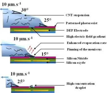
inter-Figure 2. Schematic view of the capillary assembly process.
electrode gaps. Interdigitated geometry was used to create an array of 40 × 18 gaps cm−2. Several electrode designs have been tested: rectangular or triangular electrodes as seen in the inset on figure3. The electrode width ranged from 2 to 50µm and the inter-electrode gap ranged from 2 to 12µm.
A 300 nm silicon nitride (Si3N4) layer was deposited by
plasma-enhanced chemical vapor deposition (PECVD) on the DEP electrodes in order to separate the DEP electrodes from the CNT suspension (figure1(b)). As the CNT suspension is electrically insulated from the DEP electrode, the CNTs are not damaged during the assembly process and electrochemical reactions between the DEP electrodes are avoided even when applying high voltages. A photoresist layer (500 nm AZ Lor 3A photoresist) was spin-coated and patterned with cavities above the gaps of the DEP electrodes (figure 1(c)). The geometry of these cavities can be tuned to control the shape, length and width of the final CNT connections. A 100µl droplet of well-dispersed CNT suspension was poured onto the photoresist. A function generator was plugged into the DEP electrodes to deliver localized strong electric field gradients. Using a motorized stage, the meniscus was scanned at a controlled velocity over the patterns and under electrical stimulation of the buried electrodes (figures1(d) and (e)). The scanning speed of the meniscus and the operating temperature are precisely controlled in order to tune the deposition parameters (figure2).
The photoresist layer was then properly removed. A lift-off process was used to pattern independent pairs of electrodes (Cr 10 nm/Au 90 nm). Those electrodes were designed to connect the CNT assembly sites individually (figure1(g)). An SEM image of a typical wafer prepared using this process flow is presented in figure 3. Both individual electrode pairs (white) and buried DEP electrodes (bright gray) are visible . Finally, the CNT connections can be suspended by selective wet etching of the silicon nitride layer under the CNT carpet using hydrofluoric acid solution (5%, 1 min 30) followed by a critical point drying (CPD)
1 mm
300µm DEP Electrodes
Figure 3. SEM image of a large array of individual electrodes connecting the CNT carpet (figure1, step (g)). Different gaps and shapes were used for the connection electrodes. The DEP electrodes can be seen under the Si3N4layer in bright gray.
step (figure 1(h)). This last step generates large arrays of CNT-based suspended nanocarpets.
3. Dielectrophoresis and capillary assembly
CNTs can be approximated by prolate spheroids [27] as their cylindrical shape exhibits a high aspect ratio. This approximation allows us to use the analytical expression of the DEP force [28]:
E
FDEP =23πεmlr2Re[F(ω)]∇ EE2
where εm is the medium permittivity, I is the CNT length,
r is the CNT radius, ∇ EE is the gradient of the electric field and F(ω) is the Clausius–Mossotti (CM) factor. The CM factor is determined by the frequency, the permittivities and conductivities of the medium and the CNTs. In order to attract CNTs towards high electric field gradients, the CM factor has to be positive which is achieved when using a 100 kHz signal. The choice of the resonant frequency value was such as to avoid both the dielectric breakdown and electrolysis phenomena in the CNT solution. Therefore, the DEP assembly process was performed using a 40 Vpp
sine signal (i.e. the lowest applied voltage which caused a significant CNT alignment) at 100 kHz. The highest electric field gradient is observed at the inter-electrode gap. Yet, CNT parasitic presence at electrode edges has also been observed because of the long-axis DEP force effect [29].
When assembling the CNTs using only DEP followed by solvent evaporation it was not possible to obtain a high density of assembled CNTs. In fact, the DEP force is rapidly vanishing above the DEP electrode plane. Moreover, the very first landed CNTs shield the electric field and lower the DEP force for further CNT trapping. To circumscribe this phenomenon, we have coupled the DEP effect with another methodology, allowing the manipulation of the CNT suspension for concentrating the nanotubes precisely on the DEP gaps while keeping them trapped in a very thin liquid layer. For this purpose, capillary assembly appeared as the method of choice [30–32]. Indeed, many experimental and theoretical works dedicated to the directed assembly of
Figure 4. A disorganized deposit of CNTs obtained by capillary assembly without dielectrophoresis stimulation.
colloid solution on patterned substrates have shown how to control the assembly process parameters [32, 33]. The fine tuning of temperature and meniscus displacement over the patterns can control the pinning of the triple line on the topographical patterns. This pinning leads to a local enrichment of the suspension on these areas due to convecting flows directed towards the thin layer of liquid stretched over the pinning sites [34,35]. The CNT manipulation and alignment by the capillary assembly technique have been proved using topological [36] and temperature control [37]. In our case, the contact angle of 20◦–25◦ and assembly performed at 25◦C with a scanning velocity of the meniscus of 10 µm s−1 parallel to the cavity length turned out to concentrate the CNTs inside a droplet located in the photoresist cavities just on the top of the DEP electrodes. When the capillary assembly was performed without DEP stimulation, large amounts of disorganized and not oriented CNTs were observed in the cavities (figure4). In this case,
the sole combination of capillary forces and convective flow are driving the CNT assembly [38].
In our experiments, due to the combined use of DEP and capillary assemblies, it was possible to generate organized deposition of CNTs exhibiting good orientation and high density if needed. Finally, in this process, the alignment of the CNTs can be controlled through the electrical parameters of the DEP set-up (bias, frequency) while the density of the trapped elements could be quasi-independently adjusted by tuning the parameters of the capillary assembly set-up (T◦, scanning speed, contact angle, shape of the cavities, etc).
4. Results and discussion
The assembly parameters were chosen to create dense carpets of oriented CNTs. A suspension containing 10 mg l−1 of double-walled carbon nanotubes (DWNTs) and 10 mg l−1of a dispersing agent (carboxymethyl cellulose, CMC) was used. The speed of the capillary assembly was set to 10 µm s−1. The function generator supplied a 100 kHz and 400 mVpp
sine signal which was amplified 100 times. Large scale characterizations were performed in order to measure the CNT orientation, the density between each connection and the structural quality of the integrated CNTs. The selectivity of the deposition process has been characterized using SEM imaging (figure 5) and AFM measurements (figure 6) at different processing steps.
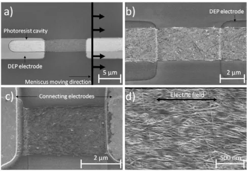
A typical SEM image of the assembled CNT layer after DEP/capillary assembly is shown in figure 5(a), while the same device after careful photoresist removal is shown in figure5(b). AFM was used to measure the height of the CNT patterns. The height of the CNT layer turned out to depend
Figure 5. SEM images of the DWNT connections at different processing steps. (a) A 26µm long cavity filled with a dense DWNT layer. The DEP electrodes are visible in bright with a gap of 10µm. (b) DWNT layer on the Si3N4film after removal of the resist (figure1(f)).
Buried DEP electrodes spaced by 5µm are visible. (c) A DWNT layer with connecting gold electrodes (5 µm gap) (step (g)). (d) Typical morphology of the obtained DWNT carpet.
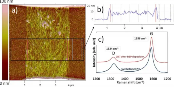
Figure 6. (a) AFM image of a typical DWNT connection. The connecting electrodes are on the top and bottom of the image. (b) Height profile of the DWNT carpet (black box in (a)) (average of 9.2 nm). (c) Averaged Raman spectra (633 nm) of the DWNT before
(as-synthesized) and after the DEP deposition.
on the size of the DEP electrode gap. In fact, the electric field gradient is higher for the smaller gaps. An average height of about 10 nm was measured for the 2µm gaps and decreased to 5 nm for the 10µm gap. It has been previously shown [15] that the diameter of the DWNTs used ranges from 1 to 3 nm. We can conclude that our CNT carpets are made of an average of 1–4 layers of CNTs mainly packed into bundles. We explain this small number by the fact that the electric field is shielded by the first CNTs which are attracted towards the Si3N4layer.
AFM measurements allowed us to evaluate approximately the CNT density. It appeared that the density of roughly aligned parallel CNTs ranged from 80 to 100 CNT µm−1. The individual electrodes were then patterned to connect each assembled CNT layers. The SEM and AFM images of such connections are shown in figures5(c) and6, respectively.
Raman spectroscopy was used to control the structural quality of the CNTs through the measurement of the ratio between the intensity of the G band (IG) and the D band
(ID) using a 633 nm laser [39]. The Raman analysis of
these connections shows a very intense peak at 1324 cm−1 and 1586 cm−1, which are related to the D and G bands, respectively. Figure6(c) is an average of the Raman spectra of a sample of CNTs before and after completing the assembly process. Typical ID/IG ratios are around 0.16, attesting
to the good structural quality of the integrated nanotubes. Very interestingly, we have observed that this ratio was systematically smaller when compared to the spectra obtained from the dried droplet of the suspension before integration. This result shows that a kind of selection is operated during the assembly, favoring the trapping of CNTs of high structural quality compared to other carbon species. We explain this phenomenon by the specificity of DEP forces with respect to the electronic properties of CNTs.
After patterning the connecting electrode level, large scale electrical characterizations were performed. Depending on the DEP electrode shape and the deposition parameters,
the yield of connected electrodes ranged from about 70% for the smallest electrodes (2µm) with the longest gap (12 µm) to 95% for the 50µm large electrodes with the smallest gap (2 µm). Those scores turned out to depend strongly on the quality of the initial CNT suspension.
The measured electrical resistances ranged from about 300 for 50 µm width and 2 µm gap connecting electrodes to about 25 k for the 4 µm width 12 µm gap connecting electrodes. The average resistivity of those CNT connections ranged from 4.4 × 10⁻⁵ m for the denser to 5 × 10⁻⁴ m for the 12 µm long connections where the CNT density is lower. This low resistivity compared to other CNT aligned layers described in the literature is in accordance with the high density and orientation score of our layers [1,7,11].
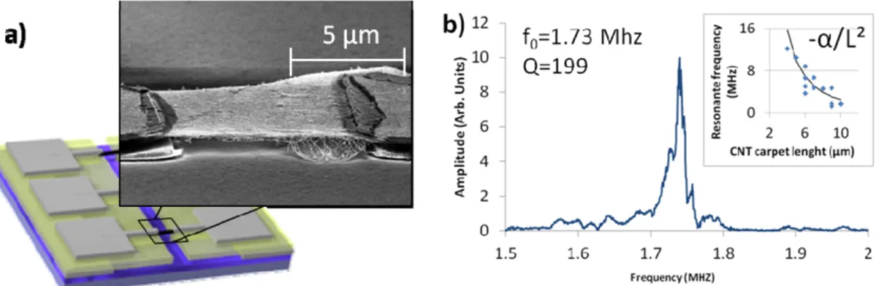
For demonstrating the wafer scale integration of these carpets of high structural quality CNTs into functional nanomechanical devices, we have optimized a release process through the wet etching of the silicon nitride layer followed by a CPD procedure. A tilted view of a typical device is shown in figure 7. After fabrication, the mechanical oscillations of the structures were analyzed using a dedicated Fabry–Perot interferometry set-up which enables the measurement of the resonance frequency and corresponding quality factor under vacuum [40]. Depending on the length of the CNT carpet, resonance frequencies ranging from 1.7 MHz for the 10µm length to 10.5 MHz for the 5µm length were measured. As expected, the resonance frequency is decreasing for increasing nanocarpet lengths [41]. A typical measurement is presented in figure7(b) and the dependence of the resonance frequency with the nanocarpet length is plotted in the inset. Quality factors ranging from 100 to 1000 have been measured for several devices. Quality factors of the longest structures are overall smaller than the one of the shortest structures (for lengths between 5 and 10 µm). This is a direct signature of higher mechanical energy dissipation by the longest structures which, when compared to the shorter ones, exhibit either
Figure 7. (a) SEM image of a suspended CNT carpet. (b) Typical Fabry–Perot measurement of one device (length: 10µm, thickness: 3 nm, width: 8µm) (inset) dependence of the resonant frequency values regarding to the nanocarpet lengths.
lower CNT densities or mechanically relaxed shapes that directly impact the quality factor.
In conclusion, we have developed an effective technique for large scale integration of oriented carbon nanotubes inside functional devices. This technique based on capillary assem-bly and buried dielectrophoresis electrodes allows aligning and assembling with high accuracy dense CNT carpets. By using this protocol large arrays of electrically independent devices such as CNT carpet-based interconnections and devices have been realized. SEM and AFM analysis showed thin, dense, aligned and precisely located CNT layers. A Fabry–Perot measurement set-up has been used to measure the mechanical behavior of suspended thin nanocarpets made of dense and aligned CNTs.
5. Experimental section
The CNT used for this work were mainly double-walled carbon nanotubes (DWNT). They have been prepared by catalytic chemical vapor deposition (CCVD) by the reaction of the decomposition of CH4 at 1000◦C (H2:CH4 atm.),
as reported earlier [42]. The catalyst was then removed by non-oxidizing HCl treatment. Transmission electron microscopy proved that the sample contained approximately 80% of DWNTs, the rest being mainly SWNTs (∼15%) and triple-walled nanotubes [15]. The DWNTs were properly dispersed using deionized water with carboxymethyl cellulose (CMC) [43]. To avoid any CNT agglomeration, the suspension was homogenized using an ultrasonic tip and then centrifugation. The suspensions obtained were well dispersed and stable. No additional purification step was performed for this study. Therefore our sample still contained some disorganized carbon species (as-synthesized CNTs).
A function generator (Tektronix AFG3102) was used to supply a controlled sine voltage. Signals are amplified with an FLC A800 amplifier (bandwidth from DC to 250 kHz). In order to control the capillary forces the substrate was placed on a motorized translation stage below a fixed glass slide at a distance of a few hundred microns. The substrate was dragged slowly parallel to the inter-electrode gap at a precisely controlled speed of 10µm s−1[44].
Raman spectroscopy was performed using a Labram HR 800 from Horiba Jobin Yvon with a 633 nm (He/Ne) laser. SEM images were obtained on an S-4800 FEG-SEM from Hitachi with a 1 kev to 30 keV acceleration voltage, depending on the sample. AFM measurements were realized with a Nanoscope 3000 from Veeco. The resistivity measurements have been performed on a Station Karl Suss PA200 and an Agilent 4142B Modular DC Source/Monitor.
The measurements of the nanotube bridges mechanical properties were achieved using a Fabry–Perot interferometry bench measurement originally developed for the characteriza-tion of silicon-based nanodevices. The samples were mounted on a small piezoelectric pellet electrically actuated by a network analyzer so that the entire substrate was vibrating. The device was placed inside a vacuum chamber pumped down to 2 × 10⁻⁶ mbar at room temperature. A 30 mW He–Ne laser was focused on the structure through the chamber window using a beam expander and a long working distance microscope objective. As in a Fabry–Perrot cavity, the laser beam is partially reflected by the structure and partially by the substrate generating interferences which are detected by a photodetector connected to the network analyzer that allows closed-loop measurement [45]. The vibration of the bridge generates periodic variation of the gap size between the bridge and the substrate which produces a periodic change in the interference intensity corresponding to the oscillation frequency of the nanostructures.
References
[1] Close G F, Yasuda S, Paul B, Fujita S and Wong H-S P 2008 Nano Lett.8 706
[2] Dai H, Wong E W and Lieber C M 1996 Science272 523
[3] Martel R, Schmidt T, Shea H R, Hertel T and Avouris P 1998 Appl. Phys. Lett.73 2447
[4] Lassagne B and Bachtold A 2010 C. R. Phys.11 355
[5] Arun A, Campidelli S, Filoramo A, Derycke V, Salet P, Ionescu A M and Goffman M F 2011 Nanotechnology
22 055204
[6] Avouris P, Chen Z and Perebeinos V 2007 Nature Nano2 605
[7] Acquaviva D, Arun A, Esconjauregui S, Bouvet D, Robertson J, Smajda R, Magrez A, Forro L and Ionescu A M 2010 Appl. Phys. Lett.97 233508
[8] Sazonova V, Yaish Y, Ustunel H, Roundy D, Arias T A and McEuen P L 2004 Nature431 284
[9] Cantoro M, Hofmann S, Pisana S, Scardaci V, Parvez A, Ducati C, Ferrari A C, Blackburn A M, Wang K-Y and Robertson J 2006 Nano Lett.6 1107
[10] Yan F, Zhang C, Cott D, Zhong G and Robertson J 2010 Phys. Status Solidib247 2669
[11] Hayamizu Y, Yamada T, Mizuno K, Davis R C, Futaba D N, Yumura M and Hata K 2008 Nature Nano3 289
[12] Morgen M, Ryan E T, Zhao J-H, Hu C, Cho T and Ho P S 2000 Annu. Rev. Mater. Sci.30 645
[13] Arnold M S, Green A A, Hulvat J F, Stupp S I and Hersam M C 2006 Nature Nano1 60
[14] Wang C, Zhang J, Ryu K, Badmaev A, De Arco L G and Zhou C 2009 Nano Lett.9 4285
[15] Flahaut E, Bacsa R, Peigney A and Laurent C 2003 Chem. Commun.1442
[16] Kang S J, Kocabas C, Kim H-S, Cao Q, Meitl M A, Khang D-Y and Rogers J A 2007 Nano Lett.7 3343
[17] Yu G, Cao A and Lieber C M 2007 Nature Nano2 372
[18] Choi S-W, Kang W-S, Lee J-H, Najeeb C K, Chun H-S and Kim J-H 2010 Langmuir26 15680
[19] Le¨ıchl´e T, Saya D, Pourciel J-B, Mathieu F, Nicu L and Bergaud C 2006 Sensors Actuators A132 590
[20] Duchamp M, Lee K, Dwir B, Seo J W, Kapon E, Forro L and Magrez A 2010 ACS Nano4 279
[21] Shekhar S, Stokes P and Khondaker S I 2011 ACS Nano
5 1739
[22] Krupke R, Hennrich F, Kappes M M and L¨ohneysen H V 2004 Nano Lett.4 1395
[23] Vijayaraghavan A, Blatt S, Weissenberger D, Oron-Carl M, Hennrich F, Gerthsen D, Hahn H and Krupke R 2007 Nano Lett.7 1556
[24] Krupke R, Hennrich F, L¨ohneysen H V and Kappes M M 2003 Science301 344
[25] Monica A H, Papadakis S J, Osiander R and Paranjape M 2008 Nanotechnology19 085303
[26] Vijayaraghavan A et al 2010 ACS Nano4 2748
[27] Venermo J and Sihvola A 2005 J. Electrostat.63 101
[28] Jones T 1995 Electromechanics of Particles (New York: Cambridge University Press)
[29] Benedict L X, Louie S G and Cohen M L 1995 Phys. Rev. B
52 8541
[30] Bowden N, Terfort A, Carbeck J and Whitesides G M 1997 Science276 233
[31] Yin Y, Lu Y, Gates B and Xia Y 2001 J. Am. Chem. Soc.
123 8718
[32] Xia Y, Yin Y, Lu Y and McLellan J 2003 Adv. Funct. Mater.
13 907
[33] Kralchevsky P A and Denkov N D 2001 Curr. Opin. Colloid Interface Sci.6 383
[34] Malaquin L, Kraus T, Schmid H, Delamarche E and Wolf H 2007 Langmuir23 11513
[35] Cerf A, Molnar G and Vieu C 2009 ACS Appl. Mater. Interfaces1 2544
[36] Xiong X, Jaberansari L, Hahm M G, Busnaina A and Jung Y J 2007 Small3 2006
[37] Ye Z, Lee D, Campbell S A and Cui T 2011 Microelectron. Eng.88 2919
[38] Fustin C-A, Glasser G, Spiess H W and Jonas U 2004 Langmuir20 9114
[39] Osswald S, Flahaut E, Ye H and Gogotsi Y 2005 Chem. Phys. Lett.402 422
[40] Carr D W and Craighead H G 1997 J. Vac. Sci. Technol. B
15 2760
[41] Nicu L and Bergaud C 1999 J. Appl. Phys.86 5835
[42] Flahaut E, Laurent C and Peigney A 2005 Carbon43 375
[43] Minami N, Kim Y, Miyashita K, Kazaoui S and Nalini B 2006 Appl. Phys. Lett.88 093123
[44] Cerf A, Thibault C, Genevi`eve M and Vieu C 2009 Microelectron. Eng.86 1419
[45] Evoy S, Riegelman M, Naguib N, Ye H, Jaroenapibal P, Luzzi D and Gogotsi Y 2005 IEEE Trans. Nanotechnol.