Université du Québec
Institut National de la Recherche Scientifique
Centre Énergie Matériaux Télécommunications
Study on the structural and dielectric properties
of epitaxial Barium Strontium Titanate (BST)
for Tunable Microwave applications.
Par
Marwa Ahmed Mohamed Ismail
Thèse présentée pour l’obtention du grade de
Philosophiae doctor (Ph.D.)
en sciences de l’énergie et des matériaux
Jury d’évaluation
Président de jury
et examinateur interne
Serioja Tatu
Professeur, INRS-ÉMT
Examinateur externe
Richard Clergereaux
Professeur, Université Paul Sabatier
Examinateur externe
Nadi Braidy
Professeur, Université de Sherbrooke
Directeur de recherche
Mohamed Chaker
Professeur, INRS-ÉMT
ABSTRACT
The future generation of active telecommunication devices may benefit a lot from components based on ferroelectrics. These tunable microwave devices require thin film ferroelectrics with specific material characteristics such as high dielectric constant that allows reducing the size of the devices, high tunability typically more than 50% for few kV.cm-1, low dielectric loss lower than 0.01 in order to minimize signal attenuation, high
Figure-of-Merit (FOM) at microwave range of frequencies (300 MHz to 300 GHz). In order to achieve these characteristics, high quality thin films, better understanding of the material properties and improvement of device designs are needed.
The challenge in the recent years is the difficulty to obtain thin films with low dielectric loss and high tunability at the same time. This step is crucial for integrating thin film in tunable microwave devices such as phase shifters, tunable resonators, filters, and tunable antenna. The most promising ferroelectric for this kind of applications is Barium Strontium Titanate, Ba0.6Sr0.4TiO3 (BST) that can have a Curie temperature around room
temperature and a dielectric constant that can be varied by more than an order of magnitude under an electric field, but that generally exhibit a relatively high level of losses at high frequency.
In this thesis high quality of BST thin films were deposited on MgO substrates by mean of pulsed laser deposition (PLD), in order to study the influence of the film microstructure on the microwave characteristics of the material. We investigated the influence of the deposition parameters such as laser fluence, laser repetition rate, substrate temperature, oxygen background pressure, substrate material type and orientation, and BST target composition on the BST thin films characteristics. Base on this first extensive study, we try to optimize the BST thin film properties by using buffer layers and doping with different elements (Mg, Ni, Mo, Fe, and Ti) in order to obtain low dielectric loss (tan δ) and high tunability at the same time.
These extended studies yielding to epitaxial, textured, and polycrystalline BST films revealed that there is a strong correlation between the microstructure properties and the microwave properties of BST thin films, that highlights the important influence of the crystal quality and lattice parameter on the microwave characteristics of the films, such correlation found between the lattice parameter and rocking curve FWHM, the rocking
curve FWHM and tunability, the lattice parameter and tunability, and dielectric loss and tunability. These observations helped to better understand the correlations between the dielectric characteristics and the material structural properties. The relation between the tunability and the material lattice parameter was found to obey to the Landau-Devonshire theory whereas the dielectric losses are found to be either intrinsically linked to the tunability or influenced by the presence of a large stress gradient at the substrate interface.
The optimum conditions for depositing epitaxial BST thin films on MgO (100) substrates were found to be at 10 Hz for laser repetition rate, 1 J/cm2 for laser fluence, 65 mm for
target substrate distance, 10 mTorr oxygen pressure, 800°C deposition temperature and post annealing conditions of 1050°C for 3 hours. In these conditions the rocking curve full-width at half-maximum obtained is of ~0.3, one of the best obtained so far for BST thin films. Interestingly, the BST Figure of Merit (FOM, ratio of tunability on the dielectric losses) of epitaxial and polycrystalline films are found to be comparable, due to high level of losses on highly epitaxial films. For example, the film deposited at 500°C is polycrystalline with a low tunability of 20%, low dielectric loss of 0.025, and a FOM of ~7.5; while the best crystal quality film ( of 0.23°) has the highest tunability of 75% and also the highest dielectric loss of 0.1 but it has a FOM of ~7.
The BST-0.6 epitaxial thin film characteristics were further improved using specific design of experiments, intended to reduce the level of stress of epitaxial films. Using, for the first time, ion implantation of Mg on epitaxial thin films and post-implantation annealing, the BST Figure of Merit was improved from ~10 to 17 (tunability of 60% and dielectric loss of 0.035 at 3 GHz and 10 V.µm-1). Our results proves that whereas
tunability and losses seem to be intrinsically linked for BST alone, ion implantation gives the opportunity to decrease the level of losses while maintaining a relatively high tunability of the material. This work provides a better understanding of the performance of BST material at microwave frequency and will help to reach the targeted ferroelectric properties for its integration into functional tunable microwave devices.
ACKNOWLEDGEMENTS
I would like to express my gratitude to my supervisor Prof. Mohamed Chaker without his help, guidance, valuable critiques, encouragement and financial support this work might not have been possible. The financial support provided by the INRS is also gratefully acknowledged.
I would like to express my sincere appreciation to the committee members for taking their valuable time to evaluate this research work.
I am deeply grateful to Sebastien Delprat for his guidance, instructive suggestions, useful discussions, helpful advice and thesis correction.
I would like to thank Boris Le Drogoff for his help in optimization of the photolithography process. Also I would like to thank the following people who have helped me along the long path of my PhD research: the LMN group, especially Etienne Charette, Amine Zitouni, Pierre-Paul Mercier, and Alex Boutin for technical help, Catalin Harnagea for AFM measurements, Christophe Chabanier for XRD, XPS measurement, Martin Chicoine from the University of Montréal for ERDA and RBS measurements.
Also, I would like to thank Paul-Francois Ndione, Mohammed Soltani, Jaeho Oh, Irina Stateikina, Riad Nechache for their valuable discussions.
Finally I would like to thank my family for their love and support.
Contents
Title ... I Abstract ... III Acknowledgements ... V List of Figures... XII List of Tables ... XIX Glossary ... XXI List of Terms ... XXII
Introduction ... 1
Telecommunication domain ... 1
Ferroelectrics for telecommunications ... 3
Statement of purpose ... 6
Presentation of the thesis ... 6
Chapter 1. Barium Strontium Titanate, a ferroelectric material for microwave applications ... 9
Introduction ... 9
1.1. General properties of ferroelectrics ... 9
1.1.1. Pyroelectricity, Piezoelectricity, Ferroelectricity ... 9
1.1.2. Mechanisms of polarization ... 12
1.1.3. Electrical properties of ferroelectrics ... 16
1.1.4. Paraelectric and Ferroelectric phases ... 18
1.2. Dielectric constant properties of BST ... 19
1.2.1. Dielectric constant and tunability of bulk BST ... 20
1.2.2. Landau theory ... 21
1.2.3. Dielectric constant and tunability of BST thin films ... 23
1.2.4. Landau–Devonshire model ... 25
1.2.5. Flexoelectricity ... 29
1.3. Dielectric loss properties of BST ... 32
1.3.1. Dielectric Loss of bulk BST ... 33
Conclusion ... 37
Chapter 2. Epitaxial growth of BST thin films ... 39
Introduction ... 39
2.1. Deposition conditions of epitaxial BST ... 39
2.1.1. Growth mode ... 39
2.1.1.a. Polycrystalline thin film ... 40
2.1.1.b. Epitaxial thin film ... 41
2.1.2. Choice of the substrate ... 42
2.1.3. Deposition method ... 43
2.2. Pulsed Laser Deposition ... 44
2.2.1. Mechanism of pulsed laser deposition ... 45
2.2.2. Advantages and drawbacks of PLD ... 46
2.2.3. Deposition parameters of BST film grown by PLD ... 47
2.3. Material characterization methods ... 49
2.3.1. Rutherford backscattering spectroscopy (RBS) ... 49
2.3.2. X-ray diffraction - (XRD) ... 51
2.3.2.a. scan ... 52
2.3.2.b. Rocking curve ... 54
2.3.2.c. Phi Scan ... 54
2.4. PLD parameters study, influence on microstructure ... 56
2.4.1. Effect of Laser fluence (Laser energy density) ... 56
2.4.1.a. Varying Laser spot area ... 58
2.4.1.b. Varying Laser energy ... 59
2.4.1.c. Constant laser fluence (1 J/cm2) ... 61
2.4.2. Effect of Laser Repetition Rate ... 62
2.4.3. Effect of BST-x Composition (x=0, 0.3, 0.5, 0.6, 0.7, 1) ... 66
2.4.4. Effect of substrate temperature ... 69
2.4.6. Effect of substrate material and orientation (MgO, LAO, Al2O3) ... 75
2.4.6.a. Influence of the substrate material ... 76
2.4.6.b. Influence of MgO substrate orientation ... 78
Conclusion ... 81
Chapter 3. Microwave characterization of BST thin films ... 84
Introduction ... 84
3.1. Microwave domain ... 84
3.1.1. Waveguides / Devices ... 84
3.1.2. Scattering parameters ... 87
3.1.3. Material characterization parameters ... 89
3.2. Thin films characterization method ... 90
3.2.1. MW characterization device and method ... 90
3.2.2. MW devices fabrication ... 94
3.2.2.a. Photolithography process optimization ... 95
3.2.2.b. Microfabrication process ... 97
3.2.3. MW diagnostic calibration ... 99
3.2.4. IDC Microwave characterization of BST thin film ... 101
3.3. PLD parameters optimization (MW properties) ... 106
3.3.1. Effect of the Laser fluence ... 106
3.3.1.a. Varying the laser spot area ... 106
3.3.1.b. Varying the laser energy ... 107
3.3.1.c. Constant laser fluence (1 J/cm2) ... 109
3.3.2. Effect of Laser Repetition Rate ... 110
3.3.3. Effect of BST-x Composition (x=0, 0.3, 0.5, 0.6, 0.7, 1) ... 111
3.3.4. Effect of substrate temperature ... 113
3.3.5. Effect of oxygen background pressure ... 116
3.3.6. Effect of substrate material and orientation ... 116
Chapter 4.
Correlation between microstructure and microwave properties of BST thin films
... 123
4.1. Synthesis of BST results ... 124
4.1.1. Correlation between lattice parameter and FWHM of rocking curve ... 124
4.1.2. Correlation between FWHM of rocking curve and tunability ... 125
4.1.3. Correlation between lattice parameter and tunability (Landau–Devonshire model) ... 126
4.1.4. Correlation between dielectric loss and tunability ... 128
4.1.5. Interpretation ... 129
4.2. Optimization of BST properties ... 131
4.2.1. Effect of a buffer layer on BST thin film properties ... 131
4.2.1.a. Literature review ... 131
4.2.1.b. Effect of BTO buffer layer thickness on epitaxial BST thin film properties ... 132
4.2.1.c. Effect of buffer layer material (BST-x with x=0 to 1) ... 136
4.2.2. Doping with different materials ... 142
4.2.2.a. Literature review ... 142
4.2.2.b. Doping with different elements ... 143
4.2.3. Doping with Mg using ion implantation ... 147
4.2.3.a. Literature review ... 147
4.2.3.b. Experimental conditions ... 148
4.2.3.c. Effect of the post-implantation annealing ... 150
4.2.3.d. Effect of Mg implantation Energy ... 154
4.2.3.e. Effect of Mg implantation dose ... 156
4.3. General Synthesis of BST results ... 159
4.3.1. Correlation between lattice parameter and tunability (Landau–Devonshire model) ... 160
4.3.2. Correlation between dielectric loss and tunability ... 161
Conclusion ... 164
Conclusion and Perspective ... 169
Résumé ... 177
List of Figure
INTRODUCTION
Figure.I.1: Microwave spectrum and application………...2 Figure I.2: The number of papers published versus year of publishing, and the number of patents versus the year………2
CHAPTER 1
Figure 1.1: Classification of crystals showing the classes with piezoelectric, pyroelectric, and ferroelectric effects………..10 Figure 1.2: Perovskites ABO3 with the atomic orbitals that contribute to covalent bonding
(oxygen atoms in the unit cell are labeled O1, O2, O3, the remaining oxygen atoms are
related to those by the repeat vectors of the crystal, indicated as a1, a2, a3). The px, py, pz orbitals of the three O atoms and the dx2−y2, d
3z2−r 2 orbitals of the B atoms that
participate in the formation of covalent bonds in the octahedron are shown schematically……….………...………11 Figure 1.3:Polarizability as a function of frequency for a typical dielectric material……..14 Figure 1.4: Real (dash line) and imaginary (plain line) part of the dielectric constant of BaTiO3 bulk ferroelectric ceramics (identified as 1) and Ba0.25Sr0.75TiO3 (BST) bulk
paraelectric ceramics (identified as 2) as a function of frequency)……….15 Figure 1.5:Schematic illustration of the variation of the dielectric constant r and the spontaneous polarization (Ps) as a function of temperature for three typical ferroelectric crystals: (a) Barrium titanate (BaTiO3) with Tc = 120°C, (b) Potassium dihydrogen
phosphate (KDP, KH2PO4) with Tc = -150°C, and (c) Potassium Sodium
tartrate-tetrahydrate (Rochelle Salt, KNaC4H4O6-4H2O) with Tc =
24°C………..……..….16 Figure 1.6:typical ferroelectric hysteresis loop………...17 Figure1.7:Free energy of perovskites ABO3 in paraelectric (a, b) and in ferroelectric (c, d,
e) phases ………19 Figure 1.8: Typical field dependence of the dielectric permittivity of Ba0.6Sr0.4TiO3 on the
electric field……….20 Figure 1.9: Dependencies of electric-field and the dielectric constant for BST film…………..…22 Figure. 1.10: Field dependence of the dielectric permittivity plotted for β = 8×10⁹ JC−4m5
Figure 1.11: Temperature dependence of the dielectric permittivity in ceramic and thin film………..….24 Figure 1.12: Definition of the crystallographic directions with respect to the film and the substrate………..25 Figure 1.13: classification of the loss mechanisms………..…………..33
CHAPTER 2
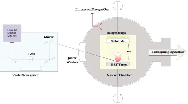
Figure 2.1: A schematic representation of several stages in the formation of a thick polycrystalline film on a substrate……….40 Figure 2.2: Film growth modes: a) Layer-by-layer (Frank-Van der Merwe), b) 3D island (Volmer–Weber), c) 3D island layer (Stranski–Krastanov) and (d) step flow…………....42 Figure 2.3:PLD setup used for synthesis of BST thin films on MgO………...…45 Figure 2.4: thickness of BST thin film (deposited on 3” diameter Si wafer) versus the distance traveled from the center of the 3” diameter of Si wafer. The thickness was measured by taken SEM images of the wafer cross section………...48 Figure 2.5: RBS and ERDA set up………44 Figure 2.6: RBS spectra simulated and measured of Ba0.6Sr0.4TiO3 thin film deposited on
MgO substrate……….51 Figure 2.7: schematic diagram of different types of scans using XRD………...…..52 Figure 2.8: XRD spectra of (scan of single phase BST-0.6 thin film grown on MgO single crystal substrate………...53 Figure 2.9: lattice parameter for BST thin film on MgO substrate. ………...53 Figure 2.10: Rocking curves of epitaxial and textured BST thin film deposited on Mg…55 Figure 2.11: Phi scan of BST thin film and MgO single crystal substrate showing cube on cube in-plane alignment……….…55 Figure 2.12.a: Deposition rate as a function of laser fluence (by increasing the laser energy at constant laser spot area)……….58 Figure 2.12.b: Deposition rate as a function of laser fluence (by decreasing the laser spot area at constant laser energy)……….58
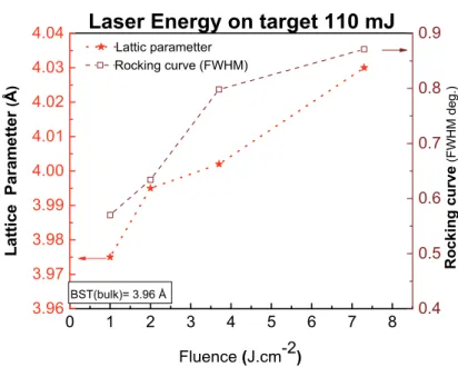
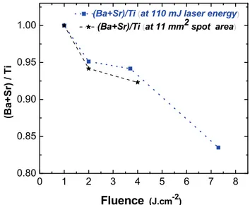
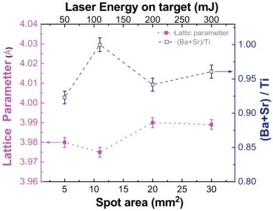
Figure 2.13: lattice parameter and rocking curve FWHM as a function of laser fluence.59 Figure 2.14: lattice parameter and rocking curve FWHM as a function of laser fluence.60 Figure 2.15: (Ba+Sr)/Ti ratio as a function of the laser fluence………60 Figure 2.16: lattice parameter and (Ba+Sr)/Ti ratio as a function of 1J/cm2 laser
fluence………..61 Figure 2.17: XRD patterns of, a.) rocking curve (-scan), b.) Phi scan, of BST-0.6 thin film on MgO single crystal substrate deposited by PLD at 2Hz and 50Hz laser repetition rate………64 Figure 2.18.a: BST films rocking curve and Phi scan FWHM as a function of laser repetition rate (2, 10, 20, and 50 Hz)………...65 Figure 2.18.b: BST films lattice parameter as a function of laser repetition rate (2, 10, 20, and 50 Hz)………..65 Figure 2.19.a: Rocking curve of BTO, BST-0.7, BST-0.6, and BST-0.3 grown on MgO substrate………..67 Figure 2.19.b: Scan (rocking curve) FWHM and Phi scan FWHM of BTO, BST-0.7, BST-0.6, BST-0.5, and BST-0.3 grown on MgO substrate………...68 Figure 2.20: Lattice parameter of (BTO, BST-0.7, BST-0.6, BST-0.5, BST-0.3, STO) thin films grown on MgO substrate. ………68 Figure 2.21: rocking curve (-scan) of BST thin films deposited on MgO substrate at deposition temperature 750, 800, 850, 900, and 950°C………71 Figure 2.22: rocking curve (FWHM), and Phi scan (FWHM) of BST thin films deposited on MgO substrate as a function of deposition temperature………...71 Figure 2.23: lattice parameter of BST thin films deposited on MgO substrate as a function of deposition temperature. ………73 Figure 2.24: XRD (θ–2θ) spectra of, a.) BST-0.6 grown on LaAlO3(100) substrate, and b.) BST-0.6 grown on Sapphire (0001) single crystal substrates. Also schematic diagram of the observed BST on Al2O3(0001)………77
Figure 2.25: XRD (θ–2θ) of BST-0.6 grown on alumina substrate……….….78 Figure 2.26: XRD (θ–2θ) spectra of a.) BST-0.6 grown on MgO (110) substrate, and b.) BST-0.6 grown on MgO (111) substrate……….79
CHAPTER 3
Figure 3.1 : Commonly used types of planar transmission lines (the substrate materials are denoted by gray areas, and conductors and ground planes by bold lines…………..85 Figure 3.2: Two-port network showing incident waves(a1, a2) and reflected waves (b1, b2) used ins-parameter definitions………...87 Figure 3.3: Schematic of coplanar waveguide (CPW) (side view)………..90 Figure 3.4: Schematic of coplanar interdigital capacitor (IDC) (top view)………..91 Figure 3.5: a) b) and c) Top and side view of the IDC; d) microwave electric field distribution in IDC...92 Figure 3.6: Description of the photolithography steps used to fabricate CPW devices on BST/MgO samples………....95 Figure 3.7:Cross section SEM images of SPR220 resist profile exposed with different energy density a) (100, 200, 300 and 400 mJ/cm2) using hard contact mode and
developed for 55s and b) (325, 350, 375 and 400 mJ/cm2) using vacuum contact mode
and developed for 60 sec………..96 Figure 3.8:Cross section SEM images of SPR220 resist profiles exposedat 300 mJ/cm2
and developed with different times (40, 50, 55 and 65 s)……….…96 Figure 3.9:Optical microscope image of IDC circuits with different gaps of 3, 6 and 12 µm fabricated on a BST/MgO sample………..…..99 Figure 3.10: SEM image of a 2 µm thick IDC finger with a 3 µm gap fabricated by lift-off on top of a BST thin film………99 Figure 3.11: the patterns for TRL calibration (thru, reflect, and line)………101 Figure 3.12: real and imaginary capacitance of IDC as a function of frequency and laser repetition rates, at zero bias………102 Figure 3.13: dielectric constant and the BST Loss tangent as function of frequency for different laser repetition rates, at zero bias voltage………...…..102 Figure 3.14: BST dielectric constant and Loss tangent of IDC as function of frequency, and applied voltages of 0 and 40 V. ……….104 Figure 3.15: Calculated tunability as a function of the applied voltages at different frequencies (1, 3, 6 GHZ), for a BST film deposited at 20 Hz laser repetition rate and an IDC with 3 µm gap………105
Figure 3.16: Tunability (measured at 2 GHz) as a function of the applied electric field for IDC circuits fabricated on the same BST sample with different gaps (3, 4, 8, 10 µm)...105 Figure 3.17: Dielectric constant and loss tangent (at 2GHz and 0V) as a function of the laser fluence at constant laser energy………..106 Figure 3.18: Tunability (at 2 GHz, 10 V.µm-1) and FOM as a function of the laser fluence
at constant laser energy………..107 Figure 3.19: Dielectric constant and loss tangent (at 2 GHz, 0 V.µm-1) as a function of
the laser fluence at constant spot size……….108 Figure 3.20: Tunability (at 2 GHz, 10 V.µm-1) and FOM as a function of the laser fluence
at constant spot size. ……….108 Figure 3.21: The tunability%, loss and FOM at 2 GHz as a function of the laser (spot size, energy) values keeping the laser fluence at 1 J/cm2. ………109
Figure 3.22: Dielectric constant and loss tangent (at 2 GHz, 0 V) as a function of the laser repetition rate………...111 Figure 3.23: Tunability (at 2 GHz and 10 V.µm-1) and FOM as a function of the laser
repetition rate………111 Figure 3.24: Dielectric constant (at 2G Hz, 0 V.µm-1) and loss tangent (at 2 GHz, 0 V.µm -1) of BTO, BST-0.7, BST-0.6, BST-0.5, BST-0.3, and STO thin films grown on MgO
substrate………112 Figure 3.25: Tunability (at 2 GHz, 10 V.µm-1) and Figure of Merit (FOM) of (BTO,
BST-0.7, BST-0.6, BST-0.5, BST-0.3, and STO) thin films grown on MgO substrate………113 Figure 3.26.a: dielectric properties of BST-0.6 thin film, dielectric constant and loss tangent (at 2 GHz, 0 V.µm-1) as a function of deposition temperature………114
Figure 3.26.b: Tunability (at 2 GHz, 10 V.µm-1) and FOM as a function of deposition
temperature………..114 Figure 3.27: a) Dielectric constant and loss tangent (at 2 GHz, 0V.µm-1) and b) Tunability
(at 2GHz, 10 V.µm-1) and FOM of BST-0.6 thin films grown on different substrate types:
CHAPTER 4
Figure 4.1: Omega Rocking curve (FWHM) as a function of Lattice parameter for the different sets presented in table 4.1 of BST-0.6. ………125 Figure 4 2: BST-0.6 tunability(at 2 Ghz, and 10 V/µm) as a function of the Omega rocking curve FWHM for the different sets presented in table 4.1………126 Figure 4.3: BST-0.6 tunability (at 2 GHz, and 10 V/µm) as a function of the measured lattice parameter for the different sets presented in table 4.1. The continuous and dotted lines correspond to the theoretical in-plane and out-of plane tunability (11 and 33) calculated for epitaxial films, using the Landau-Devonshire model………..…127 Figure 4.4: BST-0.6 tunability (at 2 Ghz, and 10 Vµm-1) as a function of the measured
dielectric loss for the different sets presented in table 4.1………..128 Figure 4.5: Lattice parameter of BST-0.6 thin films grown on MgO substrate with different thickness of BTO buffer layer (20 nm, 50 nm, and 100 nm)……….…133 Figure 4.6: Scan (rocking curve) FWHM and Phi scan FWHM of BST-0.6 thin films grown on MgO substrate with different thickness of BTO buffer layer (20 nm, 50 nm, and 100nm). ………133 Figure 4.7: Dielectric constant and loss tangent (at 2 GHz, 0 V.µm-1) of BST-0.6 thin
films grown on MgO substrate with different thickness of BTO buffer layer (20 nm, 50 nm, and 100 nm)………..134 Figure 4.8: Tunability and Figure of Merit (at 2 GHz, 10V.µm-1) of BST-0.6 thin films
grown on MgO substrate with different thickness of BTO buffer layer (20 nm, 50 nm, and 100 nm)………..135 Figure 4.9: Rocking curve of BST-0.6 thin films grown on MgO substrate with different buffer layer materials (BTO, BST-0.7, and STO). ………..138 Figure 4.10: lattice parameter of BST-0.6 thin films grown on MgO substrate with different material of the buffer layer (BTO, BST-0.7, BST-0.5, BST-0.3, and STO)…..138 Figure 4.11: Scan (rocking curve) FWHM and Phi scan FWHM of BST-0.6 thin films grown on MgO substrate with different material of the buffer layer (BTO, 0.7, BST-0.5, BST-0.3, and STO)………..139 Figure 4.12: Dielectric constant and loss tangent (at 2GHz and no bias) of BST-0.6 thin films grown on MgO substrate with different buffer layer materials (BST-x, with x=0, 0.3, 0.5, 0.7and 1)………..….140
Figure 4.13: Tunability and the Figure of Merit (at 2GHz, 10V.µm-1) of BST-0.6 thin films
grown on MgO substrate with different buffer layer materials (BST-x, with x=0, 0.3, 0.5, 0.7 and 1)………..…140 Figure 4.14: The lattice parameter of undoped BST and (Mg, Ni, Mo, Fe, Ti) doped BST thin films grown on MgO substrate, the green line correspond to position of undoped BST. ………145 Figure 4.15: Dielectric constant and loss tangent (at 2GHz, 0V.µm-1) of undoped BST
and (Mg, Ni, Mo, Fe, Ti) doped BST thin films grown on MgO substrate, the black and red lines correspond to position of undoped BST………146 Figure 4.16: Tunability (at 2GHz, 10 V.µm-1) and FOM of undoped BST and (Mg, Ni, Mo,
Fe, Ti) doped BST thin films grown on MgO substrate, the black and red lines correspond to position of undoped BST………147 Figure 4.17: ERDA results of Mg implanted 500nm thick BST-0.6 thin film at 50 KeV energy and 1X 10¹⁵ Mg+ ion /cm2 dose……….149
Figure 4.18: lattice parameter and rocking curve FWHM of Mg implanted BST-0.6 thin films with different post implantation annealing temperature (as implanted, 900C, 1000C, and 1150C)………151 Figure 4.19: Dielectric constant and losses of Mg implanted BST-0.6 thin films with different post implantation annealing temperature (as implanted, 900C, 1000C, and 1150C)……….152 Figure 4.20: Tunability and FOM of Mg implanted BST-0.6 thin films with different post implantation annealing temperature (as implanted, 900C, 1000C, and 1150C)…....152 Figure 4.21: lattice parameter of Mg implanted BST-0.6 thin films grown on MgO substrate with different implantation doses………...156 Figure 4.22: Dielectric constant and loss tangent (at 2GHz, 0V.µm-1) of BST-0.6 thin
films grown on MgO substrate as a function of the implantation dose……….157 Figure 4.23: Tunability and FOM (at 2 GHz, 10 V.µm-1) of BST-0.6 thin films grown on
MgO substrate as a function of the implantation dose………158 Figure 4.25: BST-0.6 tunability (at 2 Ghz, and 10 V/µm) as a function of the measured lattice parameter for the different sets presented in table 4.1 and 4.6. The theoretical in-plane and out-of in-plane tunability for epitaxial films (11 and 33), calculated using the Landau-Devonshire model, are plotted for comparison……….160 Figure 4.26: BST-0.6 tunability (at 2 Ghz, and 10 V/µm) as a function of the measured dielectric loss for the different sets presented in table 4.1.and 4.6………...……162
List of Tables
INTRODUCTION
Table I.1: Development and applications of ferroelectric material over the years………..4 Table I.2: Comparison of the properties of semiconductor GaAs, MEMs, and ferroelectric BST thin film varactors………5
CHAPTER 1
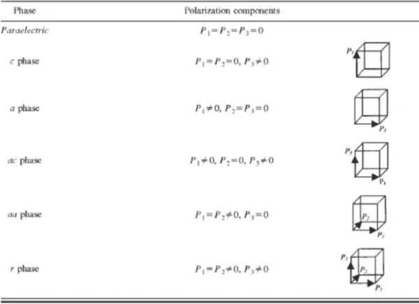
Table 1.1: The parameters for the calculation of the renormalized coefficients for BST films……….…26 Table 1.2: polarization components of the theoretically predicted phases in epitaxial ferroelectric thin films………27
CHAPTER 2
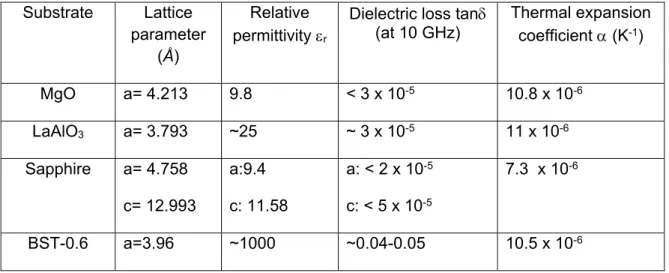
Table 2.1: Physical parameters of substrate materials commonly used in BST varactors. Note that the data are the room-temperature values………..…..43 Table 2.2: Laser spot area and laser energy were varied to maintain fixed laser fluence
at 1 J/cm2……….……61
Table 2.3: variation of lattice parameters and microstructure of the BST-0.6 thin films grown under different oxygen pressures……….75 Table 2.4: Structural properties of BST-0.6 thin films grown on different substrate types (MgO), (LaAlO3), (Sapphire), and (alumina)………78
Table 2.5: Structural properties of BST-0.6 thin films grown on different MgO substrate orientation (100), (110), and (111)………80 Table 2.6: PLD conditions for epitaxial BST thin film………..……….80
CHAPTER 3
Table 3.1: BST-0.6 dielectric constant, loss tangent (at 0 V), tunability and FOM (at 10 V.µm-1), of thin films grown under different oxygen pressures………..116
Table 3.2: Dielectric properties of BST-0.6 thin films grown on different MgO substrate orientations (100), (110), and (111)………119 Table 3.3: Structural and dielectric properties of epitaxial BST thin film………..119
CHAPTER 4
Table 4.1: Description of the sample sets. For each set the values of the studied parameter are mentioned and the typical values used for the deposition of the other sets are underlined………123 Table 4.2: Bulk ceramic and thin films deposited on MgO lattice parameter (bulk and a in Å)………...136 Table 4.3: Dielectric properties of (BST0.6/ BST0.3/ MgO), and (BST0.6/ BST0.5/ MgO)……….141 Table 4.4: ionic radius of Mg, Ni, Mo, Fe, and Ti……….144 Table 4.5: Dielectric properties of Mg implanted BST-0.6 thin films with implantation energy, 50 keV, and 100 keV………..155 Table 4.6: Description of the sample sets. For each set the values of the studied parameter are mentioned and the typical values used for the deposition of the other sets are underlined………159 Table 4.7: Comparison of the dielectric properties (losses, tunability, and FOM) of this work and recently published works of BST thin-film in GHz frequency range………….164
Glossary
Pulsed laser deposition PLD
Barium Strontium Titanate BST
Micro-electrical-mechanical systems MEMS
Monolithic microwave integrated circuits MMIC
Interdigital capacitor IDC
Barium titanate BTO
X-ray diffraction XRD
Scanning electron microscopy SEM
Rutherford backscattering spectroscopy RBS
Physical vapor deposition PVD
Chemical vapor deposition CVD
Coplanar waveguide CPW
Scattering parameters S-parameters
Conformal mapping method CMM
Partial-capacitance technique PCT
LIST OF TERMS
ε Dielectric constant
Tunability
FOM Figure-of-merit
tan δ Dielectric loss
a Lattice parameter
FWHM of the rocking curve
Tc Curie temperature
E Electric field
P Dielectric polarization
ε0 Permittivity of free space
χe Electric susceptibility um Misfit strain a1 Dielectric stiffness Qij Electrostrictive coefficients Sij Elastic compliances i Stress coefficients
γi3 Stress-related flexoelectric coupling coefficients ηi3 Converse flexoelectric coefficients
μ Flexoelectric coefficient
Tc* Strained-modified Curie temperature
Tferro Temperature for the ferroelectric transition
Tm Temperature of the maximum dielectric constant
h Plank’s constant
v Oscillation frequency
Thermal expansion coefficient
F Laser fluence
D Diffusion coefficient
INTRODUCTION
Telecommunication domain
Telecommunication is one of the great revolutions of modern times. Nowadays telecommunication includes a large variety of wired and wireless technologies such as radio and microwave devices as well as cable and fiber optics. This growing network of satellites, phones and computers allow the exchange of voice, image, data and video at an increasing speed. The telecommunications domain is still expanding and the industry's revenue represent a huge share of the global economy with service revenue, for the global telecommunications industry, estimated to be 5 trillion US$ in 2013. 1
Digital mobile communication is a great achievement of recent years because it gave people an extraordinary level of mobility with the rest of the world at its fingertip. The mobile revolution has started and the next generation of mobile and wireless communications technology is emerging. The new 3G and 4G services offer the opportunity for true broadband mobile services. The requirement for future mobile and wireless networks will include new technologies able to integrate device electronics and new material technologies at the same time. This implies new research challenges in order to optimize material properties and improvement of device design for the circuits integrating these materials.
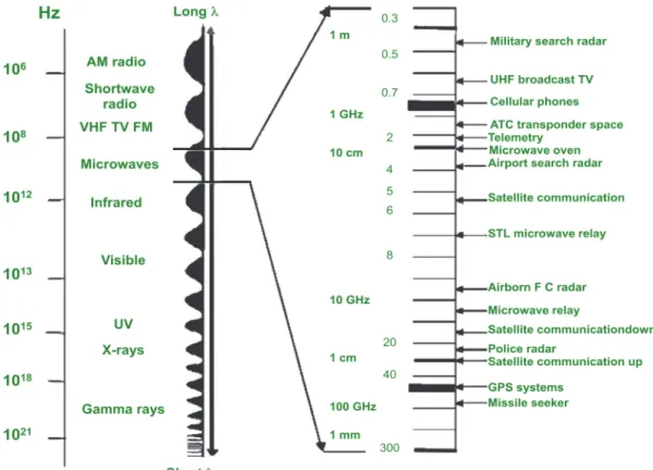
Fig. I.1 shows the position of microwave spectrum and the repartition of the different microwave bands (from 0.3 to 300 GHz) with the corresponding applications. This frequency range regroups most of wireless communication systems such as satellite communication or cellular phones which use microwave signals as a carrier. These electromagnetic waves correspond to electric length of few centimeters to few millimeters which allow compact device sizes and signal processing at high data speed. The signal processing in these devices is done through different element such as oscillators, amplifiers and tuners that uses dielectric resonators. With the recent evolution of transmitters and receivers towards more efficient bandwidth usage, the development of new dielectric material has become a large domain of research. 2
As illustrated on Fig. I.2, the number of papers published on dielectric resonator materials and technology and the number of patents filed during the last 40 years as constantly increased. More than 5000 papers have been published from 1969 to 2005 and more than 1000 patents were filed from 1975 to 2005 on the subject.
Figure.I.1: Microwave spectrum and application.2
Figure I.2: The number of papers published versus year of publishing, and the number of patents
A large portion of today’s research lies in the development of functional microwave materials in order to develop a new class of active devices for telecommunications. This research is mainly devoted to the synthesis and characterization of smart materials such as ferroelectrics which offer tunable dielectric constant under the application of an external field. These developments first require a clear understanding of the relation between structural and electrical characteristics of these materials, in particular deposited in thin film 3,4.
Ferroelectrics for telecommunications
In the quest for high-performances frequency agile (tunable) devices, ferroelectrics have many advantages such as: 5
1- Enabling the miniaturization of microwave components (dimensions are in mm), due to their high dielectric constant;
2- Enabling the integration in the thin film form with semiconductor microelectronic circuits;
3- Enabling functionalization of microwave components by the use of an external electric field which offers continuous and reversible variation of the material dielectric properties;
4- They also present high power handling and fast switching time.
Due to these unique properties, ferroelectric materials found applications in different field over the years (and particularly since the late 80s, as described in Table I.1).
For the case of tunable microwave applications, other technologies are explored, including ferrite, micro-electrical-mechanical systems (MEMS), and semiconductors. All these technologies present disadvantages that restrict their integration, especially for high frequency applications. Ferrites require the application of a magnetic field which is a technological challenge that increases the fabrication costs and the component size. They also offer slow tuning speeds and hysteresis on the material response. MEMS varactors have very low dielectric losses, however their response time is relatively slow compared to ferroelectrics or semiconductors and requires high operating voltage; they are also sensitive to environmental conditions such as air moisture, temperature and vibrations. Semiconductor technology such as GaAs varactors is presently dominant but present losses that are linearly increasing with frequency, thus limiting their applications
in tunable filters above 20 GHz. Even if semiconductor diodes have good tunability, fast tuning speed, small size and compatible with monolithic microwave integrated circuits (MMIC), they also present a large cost and low power handling capabilities.
Table I.1: Development and applications of ferroelectric materials over the years. 6, 7
1912 Ferroelectricity first described as a property of solids. 1944 Ferroelectricity discovered in ABO3-type perovskite BaTiO3.
1960s and 1970s FE semiconductor (PTC) devices developed.
FE thin films processing techniques started to emerged. mid-1980s Advancements in processing of complex ferroelectric oxides
and discovery of the high temperature superconductive oxides.
late 80s - Ferroelectric memory integrated with silicon
complementary metal-oxide semiconductor (CMOS). - Integration of microsensors with microelectronics,
emergence of the micro electro mechanical systems (MEMSs) area.
late 1990s - Introduction of polar thin films in portable telephone technologies. Mobile phones become a mass product.
- Development of BST ferroelectric material.
2010 A new family of ferroelectric materials: Me2Nb4O11 (Me = Na
and Ag) are developed.
2012 The first columnar ferroelectric liquid crystal is synthesized. Nowadays Ferroelectric films are being used in a number of
commercial, widespread products; these applications include memories, microwave electronic components, and devices with pyroelectric and piezoelectric micro-sensors/actuators.
In practice the choice of a particular technology will depend on the type of application, economic factors and material properties. Table I.2 shows a comparison between ferroelectric (BST thin film) and other competing technologies, namely semiconductor (GaAs) and MEMS.
Up to now, ferroelectric technology seems to present the most attractive characteristics with high tuning range at low voltages, high power handling, fast tuning speed and operation in a very large frequency range. The only drawback of these materials is their relatively high dielectric losses in the thin film form. For example, Barium Strontium Titanate thin films (BST) 5,8 , which is the most promising ferroelectric material for
microwave applications exhibit dielectric loss of about 0.04-0.05 in the GHz range whereas most of applications will require losses lower than 0.01 to be integrated in functional microwave devices. 9,10,11
Table I.2: Comparison of the properties of semiconductor GaAs, MEMs, and ferroelectric BST thin
film varactors.5 Semiconductor MEMS BST Tunability 2-6: 1a 1.5-3: 1b 2-4: 1 RF Loss (Q = 1 / loss tangent) 20-50 at 10GHz Very high 20-100 at 10GHz Control voltage <15 Va <50 Vb <15 V (parallel
plate type) Tuning speed 10-6 S 10-5 S 10-9 Sc
Reliability Gooda Poor Good
Cost High High Low
Power handling Poor Good Goodc
a taken from http://www.mbelectronique.fr/
b taken from Peroulis et al MTT-S Int. Microwave Symp. Digest Vol 2, p. 1117 (2003). c taken from Kozyrev et al Integr. Ferroelectr. Vol. 22, 329 (1998).
Statement of purpose
The current challenge for integrating ferroelectric thin film material such as Barium Strontium Titanate (BST) into microwave devices is to obtain low dielectric loss (tan δ) BST thin film and a large electric-field induced tuning at the same time. In this context, the main objective of this thesis is to study the influence of the film microstructure on the microwave characteristics of the BST material in order to better understand the mechanism behind dielectric losses and tunability and try to improve them.
In order to achieve this goal, we need first to understand the microstructure of the BST thin film and find out how the crystal quality (epitaxial, textured, or polycrystalline) influences the Figure of Merit (FOM, the ratio between the tunability and dielectric loss). We need to obtain different thin film characteristics using specific design of experiments and study the general correlation between microstructural and microwave properties of BST with 60% of barium (BST-0.6) thin film. This work will help to understand the mechanisms of dielectric loss and tunability and try to find ways to improve them for microwave devices applications.
This project is facing two major difficulties:
- First, achieving growth of epitaxial BST thin films. This requires careful optimization of the pulsed laser deposition (PLD) parameters in order to find the set of conditions for epitaxial growth.
- Second, fabricating interdigital capacitor (IDC) with small dimension (3 µm gap) and large thickness (2 µm thick) by photolithography, metallization and lift-off processes in order to characterize the dielectric properties of the fabricated BST thin films. This step requires an optimization of the microfabrication process in order to obtain high quality electrodes with a large aspect ratio.
Presentation of the thesis
This thesis starts with a general presentation of the telecommunication domain and briefly describes the new materials for telecommunications, and more specifically the ferroelectrics.
Chapter 1 presents the general properties of Barium Strontium Titanate, a ferroelectric material, in the context of microwave applications. The electrical properties of ferroelectrics, the mechanism of polarization and paraelectric/ferroelectric phases are presented in details. This chapter also compares the microwave properties of bulk and thin films (dielectric constant, tunability), and presents a review on Landau–Devonshire phenomenological model which provides a quantitative prediction for the dielectric properties of ferroelectrics. It also presents a phenomenological model for flexoelectricity, a theory developed to explain the dielectric constant behavior of inhomogeneously strained ferroelectric thin films. An introduction on the dielectric loss properties of BST (intrinsic and extrinsic contributions) can be found in the last part of the chapter.
The second chapter, entitled “epitaxial growth of BST thin films”, introduces the deposition of BST thin films. This chapter presents different growth modes (epitaxial and polycrystalline), the influence of the substrate, and different deposition techniques used for the epitaxial growth of BST on MgO single-crystal substrate in the literature. This section is followed by a description of the Pulsed Laser Deposition method (PLD), used to synthesize BST-0.6 thin films in this study, this includes the experimental setup and the influence of the different deposition technique parameters. The second part of this chapter concerns the material characterization methods, where the different diagnostics used to characterize the microstructural properties of the BST films are exposed. These diagnostics include scanning electron microscopy (SEM), atomic force microscopy (AFM), Rutherford backscattering spectroscopy (RBS) and X-ray diffraction (XRD) techniques. The last part of the second chapter presents experimental results on the microstructural properties of films deposited under different PLD conditions, namely the laser fluence, laser repetition rate, BST target composition, substrate temperature, oxygen background pressure, substrate material type and orientation.
The following chapter (Chapter 3, entitled “Microwave characterization of BST thin films”) is divided into three parts. The first part presents the domain of microwave with introductions to waveguides, scattering parameters, and thin film microwave parameters. The second part describes the microwave characterization device and method used in the present study to extract the dielectric constant, dielectric loss, tunability, and Figure
of Merit of BST thin film. This section includes devices fabrication (photolithography process optimization, microfabrication process), microwave diagnostic calibration, and interdigital capacitor (IDC) diagnostic description. In the last part of the chapter, the measured microwave properties of the films will be presented at the end of the chapter 2 and discussed. These results present the influence of different PLD deposition parameters (laser fluence, laser repetition rate, BST target composition, substrate temperature, oxygen background pressure, substrate material type and orientation) on the microwave properties of BST thin film.
The chapter 4 (“Correlation between microstructure and microwave properties of BST thin films”) presents general correlations between microstructural properties and the microwave properties of BST-0.6 thin film presented at the end of chapter 2 and 3. Different correlations (between the lattice parameter and rocking curve FWHM, the rocking curve FWHM and tunability, the lattice parameter and tunability and between dielectric loss and tunability) are presented and discussed in order to better understand the important material parameters for the tunability and a better understanding of the origin of the dielectric loss in BST-0.6 thin film. These observations are then used as a guide to optimize the BST-0.6 thin film for microwave applications, the goal being to obtain BST lattice parameter as close as possible to the bulk value while minimizing the film stress. This optimization, presented in the second part of the chapter, consists in the deposition of a buffer layer (thickness of a Barium Titanate (BTO) buffer layer, influence of the buffer layer material) and doping (through co-deposition of BST and a doping material by PLD and by ion implantation) and the related structural and microwave properties of epitaxial BST thin film. This chapter ends with a general synthesis on BST thin film properties (structural and electrical characteristics) regrouping all the different BST thin films synthesized during this study.
The thesis ends with the presentation of the conclusions and perspective of the presented work.
CHAPTER 1:
Barium Strontium Titanate, a ferroelectric
material for microwave applications
Barium Strontium Titanate is part of the ferroelectrics, a class of high dielectric permittivity materials characterized by a transition from a polar (ferroelectric) phase to a nonpolar (paraelectric) phase at a temperature at which their dielectric permittivity presents a maximum (called the Curie temperature). The term ferroelectricity was chosen by analogy with ferromagneticity: while ferromagnetic effect occurs in presence of a magnetic field, the ferroelectric phenomenon happens in the presence of an electric field. Below the Curie temperature (Tc) ferroelectrics exhibit a spontaneous electric
polarization and a hysteresis loop of the dielectric constant as a function of the electric field E; above Tc they present a continuous change of the dielectric constant as a
function of E. These unique properties make ferroelectrics very attractive for the conception of microwave devices and especially active devices in which the microwave signal could be controlled by an external voltage.
1.1. General properties of ferroelectrics
1.1.1. Pyroelectricity, Piezoelectricity, Ferroelectricity
Pyroelectrics are a class of materials in which heat can generate electricity or electricity can generate heat. Pyroelectricity is a phenomenon known for a very long time: the philosopher Theophrast described it in 314 bc in relation to a stone (supposedly tourmaline) that was able to attract bits of wood when heated. It took more than 20 centuries to relate this phenomenon to electricity and few more centuries to develop a theory explaining the observed effect. It is now well known that pyroelectricity is closely related to the crystallographic structure of the material. Many physicists studied this kind of materials and discovered other related properties. In 1880 Pierre and Jacques Curie discovered piezoelectrics, a class of materials in which mechanical stress can generate electricity or electric filed can generate mechanical stress. In 1921, Valasek discovered the ferroelectric phenomena in the Rochelle salt (potassium-sodium tartrate tetrahydrate, KNaC4H4O6–4 H2O), a colorless crystalline compound with an orthorhombic structure
ferroelectric compound was identified: Potassium-Dihydrogen Phosphate (KDP). And another decade later barium titanate (BaTiO3) was added to the list of ferroelectric
materials that is still growing nowadays.
Pyroelectric, piezoelectric or ferroelectric materials are characterized by a net electric polarization. In general, all materials undergo a small change in dimension when exposed to an external force, such as an electric field, a mechanical stress, or a change in temperature. Depending on the material structure, such a small change in dimension may result in a change in electric polarization and hence give rise to the occurrence of the ferroelectric, piezoelectric, or pyroelectric effects. Materials exhibiting these effects are polar and crystalline, or polycrystalline. The specific symmetry of the unit cell determines whether the crystal exhibits ferroelectric, piezoelectric, pyroelectric, or electro-optic effects.
Figure 1.1: Classification of crystals showing the classes with piezoelectric, pyroelectric, and ferroelectric effects.
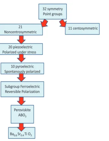
The existence of pyroelectricity in a material requires that its molecular structure have a nonzero dipole moment, no center of symmetry and must have either no axis of
rotational symmetry or a single axis of rotational symmetry that is not included in an inversion axis. On the basis of the symmetry elements, there are 32 point groups or classes. The 32 point groups are subdivisions of seven basic crystal systems, these seven basic crystal systems are triclinic, monoclinic, orthorhombic, tetragonal, trigonal (rhombohedral), hexagonal, and cubic.12 Of these 32 classes, 11 classes are
centrosymmetric and 21 classes are noncentrosymmetric possessing no center of symmetry. Only 20 classes of noncentrosymmetric crystals exhibit piezoelectric effects. Only 10 of these 20 classes possess spontaneous polarization, being permanently polar and thus exhibiting piezoelectric as well as pyroelectric effects. There is a subgroup within these 10 classes that possesses spontaneous polarization and reversible polarization and that can have ferroelectric, piezoelectric, and pyroelectric effects.
As shown on Fig. 1.1, Barium Strontium Titanate (or BST of formula BaxSr1-xTi O3)has a
perovskite structure and is one of the few ferroelectric materials that exhibit spontaneous polarization with applied electrical field due to the atomic displacement of the body-centered atom (Ti) in the perovskite (ABO3) structure.
Figure 1.2: Perovskites ABO3 with the atomic orbitals that contribute to covalent bonding (oxygen
atoms in the unit cell are labeled O1, O2, O3, the remaining oxygen atoms are related to those by the
repeat vectors of the crystal, indicated as a1, a2, a3). The px, py, pz orbitals of the three O atoms and
the dx2−y2, d3z2−r 2 orbitals of the B atoms that participate in the formation of covalent bonds in the
The chemical formula of perovskites is ABO3, where A is the easily ionized element (in
the case of BST, Ba or Sr atoms occupy the site A) and B is the element located at the center which is bonded to oxygen atoms (in case of BST, Ti atom occupies the site B). The basic unit cell is shown in Fig. 1.2 with the corresponding atomic orbitals. Bonding in the xy plane is accomplished through the overlap between the px and py orbitals of the first (O1) and second (O2) oxygen atoms, respectively, and the dx2−y2 orbital of B; bonding
along the z axis is accomplished through the overlap between the pz orbital of the third (O3) oxygen atom and the d3z2−r2 orbital of B. The A atoms provide the necessary number
of electrons to satisfy all the covalent bonds. Thus, the overall bonding involves both strong covalent bonds between B and O, as well as ionic bonds between the B–O units and the A atoms 8.
1.1.2. Mechanisms of polarization
In a dielectric subject to an electric field E, the dielectric polarization density P is defined as:
χ ………...………..Eq. 1.1
where ε0 is the electric permittivity of free space ( 8.85 10 / ) and χe is the electric susceptibility.
The electric susceptibility χe of a medium is hence a measure of how easily it polarizes in response to an electric field. It is related to the relative permittivity of the material εr by
χ 1 ………... Eq. 1.2
The electric displacement D is related to the polarization density P by
1 χ ……….. Eq. 1.3
The polarization P of a dielectric material with the density Nj is the sum of all the individual dipole moments pj :
∑ ……...………….. Eq. 1.4
The dipole moment induced by an electric field E can be expressed as: …………...……..…… Eq. 1.5
where α is the polarizability of an atomic dipole.
The relation between the susceptibility (χ) and the polarizability (α) is given by:
ε0χ = Njαj . ………...…… Eq. 1.6
In general, there are five different mechanisms of polarization which can contribute to the dielectric response:
Electronic polarization
This mechanism is common in all dielectric materials. By applying an electric field, the center of the negative charge within the atomic structure is shifted relatively to the position of the positive nucleus and creates a dipole. The electronic polarizability αe is temperature-independent. And large atoms have a large electronic polarizability.
Ionic polarization
This mechanism is observed in ionic crystals. By applying an electric field, the cations and anions will be displaced in opposite direction and will cause a net dipole moment. Orientation polarization
This mechanism only exists in materials that contain permanent dipoles moments. As an electric field is applied the dipole moments rotate to align themselves with the field. This type of polarization (due to alignment of permanent dipoles) is sensitive to thermal vibrations and will decrease as the material is heated.
Space charge polarization
This mechanism could exist in dielectric materials which show spatial inhomogeneities of charge carrier densities. It occurs when mobile charges within the material are impeded by interface such as grain boundaries and are not discharged at an electrode.
Domain wall polarization
The domain walls separate regions of different oriented polarization. The motion of a domain wall takes place when a strong electric field is applied to the material that favor domains orientation along the electric field lines.
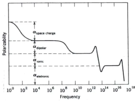
In a dielectric, the total polarization comes from the different mechanism contributions and is dependent on the frequency. Fig. 1.3 shows the typical polarizability of materials as a function of frequency.13 Electronic and ionic polarization are called intrinsic
contributions, they show contributions up to very high frequencies and exhibit resonance effects. The other mechanisms (orientation, domain walls, and space charge polarizations) are called extrinsic contributions and have a relaxation behavior. They tend to vanish as the frequency increases: above few tens of GHz, only the intrinsic contributions are present.
Figure 1.4: Real (dash line) and imaginary (plain line) part of the dielectric constant of BaTiO3 bulk
ferroelectric ceramics (identified as 1) and Ba0.25Sr0.75TiO3 (BST) bulk paraelectric ceramics
(identified as 2) as a function of frequency [from ref. 14]).
The dispersion of the dielectric response of each contribution leads to dielectric losses of the matter which can be mathematically expressed by a complex dielectric permittivity:
ε
ε
,iε
,,………...…… Eq. 1.7Dielectric losses are usually described by the loss tangent:
,,
,………...…… Eq. 1.8
Fig. 1.4 shows the real (’) and imaginary (’’) parts of the BaTiO3 and Ba0.25Sr0.75TiO3
bulk ceramics, measured as a function of the frequency (from 200 MHz to 60 GHz). It is evident from this figure that large variations of the dielectric properties are observed as a function of frequency with the presence of maxima with positions depending on the material composition.
1.1.3. Electrical properties of ferroelectrics
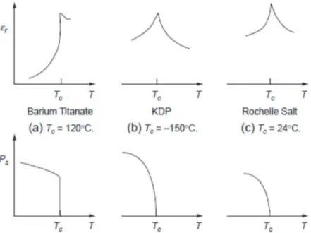
Figure 1.5: Schematic illustration of the variation of the dielectric constant r and the spontaneous
polarization of spontaneous polarization (Ps) as a function of temperature for three typical
ferroelectric crystals: (a) Barrium titanate (BaTiO3) with Tc = 120°C, (b) Potassium dihydrogen
phosphate (KDP, KH2PO4) with Tc = -150°C, and (c) Potassium Sodium tartrate-tetrahydrate
(Rochelle Salt, KNaC4H4O6-4H2O) with Tc = 24°C. 15
Ferroelectrics are pyroelectrics with a reversible spontaneous polarization. The direction of their polarization can be reversed by a sufficiently large electric field. They are characterized by their Curie temperature TC, which marks the transition between a polar
state (below TC, where they can exhibit pyroelectricity) and a nonpolar state (also called
paraelectric state, above Tc).15
The typical dielectric constant–temperature and polarization–temperature characteristics curves of three different ferroelectrics (BTO, KDP, and Rochelle salt) are shown in Fig. 1.5. This figure shows that the dielectric constant of these ferroelectric increases very rapidly to reach a maximum value at Tc and that this transition temperature can be very
different from one material to the other.
In the ferroelectric state (T < Tc), the material spontaneous polarization Ps usually increases rapidly just below the transition point and then gradually reaches a saturation
value at lower temperatures. When an electric field is applied on a ferroelectric in the ferroelectric state, the polarization P presents nonlinearities and a hysteresis as a function of the applied electric field E as shown on Fig. 1.6:
- Starting from the unpoled state and applying a small electric field, all the spontaneous
dipoles will align in the direction of the field and the polarization increases linearly with the field (from origin to point A).
- By further increasing the electric field all domains start to orient toward the direction of the field (from point A to point B) and the polarization increases nonlinearly.
- Above a certain field (and below the breakdown field), the polarization will reach a saturation state (from point B to point C), where almost all domains are aligned toward the direction of the poling field.
This process, inducing alignment of domain walls in the ferroelectric state is often called material poling.
- When the material is poled and if the electric field is gradually decreased to zero, the polarization will not go to zero but follow the path CBD, down to the remnant polarization value Pr (point D on the figure). The spontaneous polarization value Ps is defined as the intersection of line CB and the polarization axis.
Figure 1.6: Typical ferroelectric hysteresis loop.15
Going from positive electric fields to negative ones, the P-E plot will follow a hysteresis loop characterized by the remnant polarization Pr and the coercive field Ec values. Ec
corresponds to the field required to bring the polarization back to zero (distance 0R on the electric field axis). When the field is increased from negative values to zero, the
remanant polarization is reversed (point H), indicating a change in the direction of the material polarization. The hysteresis arises from the energy needed to reverse the metastable dipoles during each cycle of the applied field.
In the paraelectric state (T > Tc), the material has no spontaneous polarization and its
dielectric constant follows the Curie–Weiss relation r= C / (T-TC), where C is known as the Curie constant.16 When an electric field is applied, the polarization presents a
continuous increase (the dielectric constant decreases), followed by a saturation below material breakdown and goes back to zero when the applied field is removed.
1.1.4. Paraelectric and Ferroelectric phases
The basic electric field tuning mechanism of the permittivity can be represented by a simple mechanical spring model 17, as depicted in Fig1.7:
In the paraelectric phase (Fig.a,b)
I. The central ion oscillates about the equilibrium position and the free energy is characterized by a parabolic dependence.
II. An external electric field will shift the central ion from its equilibrium position to a new position and induce an electrical dipole.
III. When the external field is switched off the ion will go back to the equilibrium position.
In ferroelectric phase (Fig.c,d,e)
I. The central ion will shift left or right and the free energy is minimum at these positions.
II. The ion will remains in the new position (left or right) as long as no external forces are applied.
III. Under external DC field the central ion shift from left to right changing the direction of the polarization.
IV. Changing the direction of the external field will brings the ion back to its left position.
Figure1.7: Free energy of perovskites ABO3 in paraelectric (a, b) and in ferroelectric (c, d, e)
phases.17
1.2. Dielectric constant properties of BST
The two inverse permanent polarization states of ferroelectrics are very useful for applications such as non-volatile memory devices (the two states being used as the 0 and 1 binary states). But in the case of microwave devices, it is preferable to obtain a continuous change of the material properties as a function of the electric field, which occurs in the paraelectric state only. Moreover, dielectric losses are much higher in the ferroelectric state than in the paraelectric state.
The other key parameter for room temperature microwave applications is the tunability, defined as the ratio of the dielectric permittivity at zero electric field to the permittivity at a given electric field E0. The tunability is commonly described by:
………Eq 1.9
Among all the ferroelectric materials, Barium Struntium Titanate or BST-x of formula BaxSr1-xTiO3 is considered as the most promising material for electrically tunable
microwave devices applications. BST is a solid solution of SrTiO3 (STO) and BaTiO3
respectively. The adjustment of the fraction x of BaTiO3 into the solid solution is a way to
precisely define the Tc of BST. As the Ba atom substitute the Sr atoms in the STO unit
cell, the lattice parameter and Curie temperature linearly increase. In order to obtain a large tunability at room temperature, one needs to be just above ferroelectric-paraelectric phase transition. This corresponds to x fraction between 0.5 and 0.6. For instance the TC of Ba0.6Sr0.4TiO3 (BST-0.6) is about 5°C.18
1.2.1. Dielectric constant and tunability of bulk BST
Fig 1.8 shows the permittivity of bulk Ba0.6Sr0.4TiO3 material as a function of the electric
field at room temperature. The dielectric constant εr of the ferroelectric material has strong dependence on the applied electric field E0, it varies from about 10000 to 1000 (a
ratio of 1:10 corresponding to a tunability of 90%) for an electric field of 25 kV/cm (=2.5 V/µm).
Figure 1.8: Typical field dependence of the dielectric permittivity of Ba0.6Sr0.4TiO3 on the electric
1.2.2. Landau theory
19The Landau theory gives a model for the dielectric response of a bulk ferroelectrics, it is based upon an expansion of the Helmholtz free energy F with respect to the vector polarization P. For the situation where the polarization is in the direction of the electric field E applied to the material, the first two terms of this expansion are:
………Eq. 1.10a And from the equation of state
………Eq. 1.10b
it is possible to obtain a relation between the polarization and the electric field: ……….Eq.1.11
From Eq. 1.1 and 1.2, the material susceptibility is given by: χ such that χ ……...…….Eq.1.12
Hence, the relative dielectric permittivity of the material can be expressed as:
χ χ 0 ………Eq.1.13
Where χ 0 (at E=0) is the susceptibility given by
χ 0 ………Eq.1.14
According to the Landau theory, the coefficient of a ferroelectric is assumed to be a linear function of temperature and vanishes at the Curie-Weiss temperature Tc, it has the
expression:
| |
……….Eq. 1.15
where Tc and C are the Curie temperature and the Curie-Weiss constant respectively.
For ferroelectrics the Curie-Weiss constant C is about 105 K. Such a value implies high
values of the dielectric permittivity even far from the Tc. For example, at T = Tc +200 K,
from Eqs. 1.13 and 1.14 one can obtain χ 0 =500. This implies that the susceptibility of ferroelectrics (χ 1) can be approximated by .
From the value of χ 0 (or 0 , the Eq.1.13 gives the expression of χ as a function of P. This equation can also be expressed as a function of E (since χ , Eq. 1.1), which leads to a polynomial expression of the 3d order for χ :
Figure 1.9: Dependencies of electric-field and the dielectric constant for BST film.20
The parameters and being positive constants at a given temperature, this cubic equation has a negative discriminant and hence only one real solution for each electric field E. Fig. 1.10 graphically illustrates the calculation of for two values of r(0) and a β of 8 × 10⁹ J.C−4 m−5 (typical value for SrTiO
3). It shows that the Landau theory gives
a good representation of the dielectric constant variation as a function of the dielectric field for SrTiO3, with a fast decrease of the dielectric constant up to ~40 kV/cm, which
slows down above this value. It also shows that the amplitude of the variation depends on the starting value of the dielectric constant (at E=0): the higher 0 is, the higher is the variation (corresponding to the tunability).
Figure. 1.10: Field dependence of the dielectric permittivity plotted for β = 8×10⁹ JC−4m5 and for the
If we state that χ the tunability (Eq. 1.9) can be written as:
1 1 1 ……….Eq.1.17
This expression has the form where
1 3 χ 0 χ ... Eq.1.18
For weak electric fields χ χ 0 , n → 1 and is close to zero. For large electric fields n >> 1, gets closer to 1 (or 100 %). Since χ (or ) can be calculated for a given value E0, it is also possible to calculate E knowing the
parameters and of the ferroelectric. being temperature dependent, the Landau theory also allows calculating the tunability as a function of the temperature for a given electric field. In any case, it is sure that the tunability will be maximum for a given E0
when the temperature is as close as possible to the Curie temperature, the factor n being proportional to χ 0 =
| |.
1.2.3. Dielectric constant and tunability of BST thin films
Although ferroelectrics have found many applications in the bulk form (such as bulk acoustic wave resonators), in most of wireless applications, they need to be integrated as thin films in order to reduce the size and the cost of production of the active components. The problem until now for thin-film applications is that the material thin film properties are far from the one of bulk ceramics.
Dielectric Permittivity
Many groups have synthesized ferroelectric thin films since the last twenty years, and BST was one of the most investigated materials, but most of the BST thin films obtained present dielectric properties well below the ones of bulk ceramics. Fig. 1.11 compares the temperature dependence of the dielectric permittivity in BST-0.7 ceramic and thin film form. Whereas the bulk form presents a sharp peak at the Curie temperature, reaching dielectric constant values of ~20000, the thin film presents almost no transition or one that is completely flatten out and well below the expected Curie temperature with