HAL Id: hal-01807075
https://hal-univ-rennes1.archives-ouvertes.fr/hal-01807075
Submitted on 12 Jul 2018
HAL is a multi-disciplinary open access
archive for the deposit and dissemination of
sci-entific research documents, whether they are
pub-lished or not. The documents may come from
teaching and research institutions in France or
abroad, or from public or private research centers.
L’archive ouverte pluridisciplinaire HAL, est
destinée au dépôt et à la diffusion de documents
scientifiques de niveau recherche, publiés ou non,
émanant des établissements d’enseignement et de
recherche français ou étrangers, des laboratoires
publics ou privés.
Non-volatile resistive switching in the Mott insulator
(V1-xCrx)(2)O-3
M. Querre, J. Tranchant, B. Corraze, Stéphane Cordier, V. Bouquet, S.
Députier, Maryline Guilloux-Viry, M. -P. Besland, E. Janod, L. Cario
To cite this version:
M. Querre, J. Tranchant, B. Corraze, Stéphane Cordier, V. Bouquet, et al.. Non-volatile resistive
switching in the Mott insulator (V1-xCrx)(2)O-3. Physica B: Condensed Matter, Elsevier, 2018, 536,
pp.327-330. �10.1016/j.physb.2017.10.060�. �hal-01807075�
Non-volatile resistive switching in the Mott insulator (V1-xCrx)2O3
M. Querré
1,2, J. Tranchant
1, B. Corraze
1, S. Cordier
2, V. Bouquet
2,
S. Députier
2, M. Guilloux-Viry
2, M.-P. Besland
1, E. Janod
1and L. Cario
11 Institut des Matériaux Jean Rouxel (IMN), Université de Nantes, UMR CNRS 6502, 44322 Nantes (FRANCE) 2 Institut des Sciences Chimiques de Rennes (ISCR), Université de Rennes 1, UMR CNRS 6226, 35042 Rennes (FRANCE)
E-mail : [email protected]
Abstract
The discovery of non-volatile resistive switching in Mott insulators related to an electric-field-induced insulator to metal transition (IMT) has paved the way for their use in a new type of non-volatile memories, the Mott memories. While most of the previous studies were dedicated to uncover the resistive switching mechanism and explore the memory potential of chalcogenide Mott insulators, we present here a comprehensive study of resistive switching in the canonical oxide Mott insulator (V1-xCrx)2O3.
Our work demonstrates that this compound undergoes a non-volatile resistive switching under electric field. This resistive switching is induced by a Mott transition at the local scale which creates metallic domains closely related to existing phases of the temperature-pressure phase diagram of (V1-xCrx)2O3. Our work demonstrates also reversible resistive switching in (V1-xCrx)2O3
crystals and thin film devices.Preliminary performances obtained on 880 nm thick layers with 500 nm electrodes show the strong potential of Mott memories based on the Mott insulator (V1-xCrx)2O3.
Keywords: Mott insulators, V2O3, Mott transition, resistive switching, non-volatile memory, ReRAM.
1. Introduction
Resistive Random Access Memories (ReRAM) are considered as one of the most promising technologies for future non-volatile memories. They are based on resistive switching mainly related to two physical mechanisms: ionic electromigration (anionic for OxRAM and cationic for CBRAM) and thermochemical reactions (typically in NiO) [1, 2, 3]. But recently the insulator to metal transition (IMT) in Mott insulators has focused much attention due to its serious potential as an alternative mechanism for ReRAM [4]. Mott insulating state can be usually destabilized by pressure and doping into a correlated metal phase via an isostructural electronic phase transition, as shown for example in the temperature-pressure phase diagram of V2O3 in Fig. 1(a) [5].
However recent works [4, 6, 7, 8] have shown that electric field can also destabilize the Mott insulating state and trigger a non-volatile resistive switching in these materials. Studies performed on the chalcogenide compounds AM4Q8 (A=Ga,
Ge; M=Nb, V, Ta; Q=S, Se) have demonstrated that this resistive switching (RS) originates from an avalanche breakdown phenomenon [7] which causes the collapse of the paramagnetic Mott insulator state at the nanoscale [10] and results in the creation of granular conductive filaments [11].
This discovery on the chalcogenide AM4Q8 compounds
raises the question of the universal nature of this new type of non-volatile resistive switching. We have therefore sought such resistive switching in the most famous canonical narrow gap Mott insulator, namely (V1-xCrx)2O3. We report here that
this oxide Mott insulator exhibits a non-volatile resistive switching of the same physical nature as the AM4Q8
compounds. Moreover we show that the performances of a (V1-xCrx)2O3 memory cell obtained on a device mostly
compatible with microelectronics standards are very promising.
2. Material and methods
2.1. (V1-xCrx)2O3 crystals synthesis
V2O5 (Aldrich, > 99.6 %) powder was first dried at 400°C ,
then mixed with Cr2O3 (Prolabo, 99.9 %) in the 97.5 : 2.5
molar ratio, and then heat-treated at 900°C for 10h under a 95% Ar – 5% H2 gas flow. Half a gram of the obtained
(V0.975Cr0.025)2O3 powder was then placed in a silica tube
together with 40 mg of sulfur as a vapor phase transport agent. The tube was vacuum sealed, heated up to 1050°C in a temperature gradient (≈ 10°C/cm) furnace and then cooled down at -2°C/h to 900°C, before a faster cooling (-300°C/h) to room temperature. Energy Dispersive X-ray Spectroscopy analyses carried out on the obtained crystals (typical size 100 ´ 50 ´ 300 µm) indicate that the V / Cr ratio is close to the nominal value and show the absence of sulfur impurities in the crystals.
2.2. Thin film synthesis and device preparation
Thin films of (V0.95Cr0.05)2O3 were deposited by reactive
co-sputtering of V and Cr targets in Ar/O2 discharge [12],
leading to thicknesses in the 100-880 nm range. Post deposition annealing at 500°C in a reducing atmosphere yields crystallized and single-phased (V0.95Cr0.05)2O3 layers as
checked by X-Ray diffraction (XRD). In V2O3, deviation from
the ideal V/O ratio by 1.75 % lowers the magnetic ordering temperature (paramagnetic metal PM to antiferromagnetic insulator AFI transition, see Fig. 1(a)) from 155 K to 11 K [13]. But our (V0.95Cr0.05)2O3 thin films deposited on SiO2/Si
substrates and measured with four probes in a planar configuration exhibit a paramagnetic Mott insulator PMI – AFI transition temperature (158 K) very close to the expected one (175K), which indicates that they are almost stoichiometric. This prevents spurious electromigration processes associated to ionic diffusion and excludes potential OxRAM/CBRAM mechanisms. Devices based on a symetric TiN / (V0.95Cr0.05)2O3 / TiN MIM structure were subsequently
realized with via diameters in the 330 - 1600 nm range.
2.3. Electrical measurements
(V0.975Cr0.025)2O3 crystals were contacted with 17 μm gold
wires using a carbon paste (Electrodag PR-406) and then annealed in vacuum at 150 °C for 20 min to achieve a low contact resistance. The low-bias resistance was measured
using a high-impedance Keithley 236 source-measure unit. Thin film devices and crystals were connected in series with a load resistance Rload playing the role of current limiter and
ranging in the 10-80 % of the device or crystal resistance. The write-erase cycling measurements were performed using an Agilent 81150A pulse generator.
3. Results and Discussion
3.1. Resistive switching in (V1-xCrx)2O3 crystals
Figure 1(b) shows the resistance versus temperature (blue curve) measured on a (V0.975Cr0.025)2O3 single crystal grown by
the sulfur vapor transport method. Above 190K, the crystal shows an insulating behavior consistent with the expected PMI state. The transition from the PMI to the AFI phase occurs around 180 K which is again in good agreement with the value expected from the phase diagram (see Figure 1(a)). The crystal in series with a load resistance was subsequently subjected to an electric pulse (75V, 100µs at 155K). As shown in Figure 1(b), the application of this electric pulse induces a non-volatile decrease of the resistance R(T) by several orders of magnitude at low temperature (red curve). This observation reveals that the application of short electric pulses can induce a non-volatile metal-insulator transition in the Mott insulator (V0.975Cr0.025)2O3 which is reminiscent of the behavior of
AM4Q8 compounds [14].
Previous in-depth studies of GaTa4Se8 have unveiled
important features of the non-volatile resistive switching of the AM4Q8 family of compounds.This narrow gap Mott insulator
exhibits indeed an insulator to metal transition under pressure (at about 5 GPa) and becomes superconducting below
TC= 4-7K above 11 GPa [11,12]. In GaTa4Se8, Scanning
Tunneling Microscopy (STM) measurements have revealed that the non-volatile resistive switching is related to an electronic phase separation at the nanoscale [10,11]. The surface topography of pristine GaTa4Se8 crystals is
structureless, but after resistive switching some granular filamentary structures qualitatively oriented along the direction of the electric pulses appear on the surface. Spectroscopic (STS) experiments have confirmed the existence of electric-field-induced metallic nano-domains of about 30-70 nm within these granular filamentary paths. Moreover the presence of granular superconductivity at low temperature, reminiscent of the one observed under pressure, directly suggests the presence of compressed metallic nano-domains in transited crystals of GaTa4Se8 [11].
This hypothesis was further tested in the case of (V1-xCrx)2O3 using thetransition towards the AFI phase as a
probe. The phase diagram of this compound (see Fig. 1a) shows indeed that the transition temperature from the Mott insulating phase (PMI) to the AFI phase does not change much with composition or pressure. Conversely the huge variation observed under composition/pressure for the transition temperature from the metallic (PM) to the AFI phase may be used to characterized the formation under electric pulse of compressed metallic domains. Figure 1(b) compare the R(T) curves of the (V0.975Cr0.025)2O3 crystal in the pristine state (blue
curve) and after resistive switching (red curve). Both curves show the signature of the PMI-AFI transition around 180K; in the switched crystal, it corresponds to the transition of the (V0.975Cr0.025)2O3 matrix embedding the filamentary
Fig. 1 : (a) Theoretical phase diagram of (V1-xCrx)2O3 [5]. (b)
Evolution of resistance vs temperature of a (V0.975Cr0.025)2O3 crystal in
its pristine state and in a transited state. As expected the PMI-AFI phase transition occurs around 180 K in the pristine state (see blue dotted line in (a) and blue arrow in (b)). In the transited state a new transition occurs at 40 K suggesting the formation of compressed metallic domains (see red dotted line in (a) and red arrow in (b)). (c) Schematical drawing of the formation of a granular filamentary path in the transited state of a (V0.95Cr0.05)2O3 crystal containing some
compressed domains with a PM-AFI phase transition around 40 K as indicated by the red dotted line in (a).
conducting path (light blue regions in Fig.1 (c)). However a new transition is clearly observable around 40K in the R(T) curve of the switched (V0.975Cr0.025)2O3 crystal (in red).
According to the phase diagram of this system, this may be viewed as the PM ® AFI transition of (V0.975Cr0.025)2O3 under a
pressure of 30 kbar [17]. This is a clear indication of the creation of compressed metallic domains under electric field. After resistive switching the metallic domains would therefore correspond to (V0.975Cr0.025)2O3 domains under pressure, as
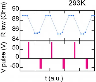
Fig. 2: Resistive switching cycles obtained at room temperature on large crystals of (V0.925Cr0.075)2O3 by applying a series of pulses
(+90V for the SET and -50V for RESET).
experiments, we may therefore infer, as sketched in Figure 1(c), that the Mott insulator compound (V1-xCrx)2O3 that has
experienced a resistive switching under electric field contains some conducting granular filamentary paths embedded in a pristine like matrix. Moreover these granular filamentary paths include some compressed regions that have undergone a Mott insulator to metal transition.
3.2. Reversible resistive switching in (V1-xCrx)2O3 crystals
Figure 2 reveals another interesting feature of the non-volatile resistive switching in (V1-xCrx)2O3. It shows that
reversible resistive switching may be obtained on crystal at room temperature using a series of voltage pulses (+90V for the SET and -50V for RESET). This observation is consistent with data obtained on AM4Q8 [6]. The RESET transition was
explained on the basis of a modeling work by the transition back of the metallic domains to the insulating state thanks to a thermal activation process enabled by self-Joule heating of the filament during the pulse [7, 16]. This reversible resistive switching opens the way to the use of the Mott insulator (V1-xCrx)2O3 as an active material of a non-volatile ReRAM
memory. However the ROFF/RON ratio on crystals is quite poor
(< 1.05), ROFF and RON being defined respectively as the
resistance values of high (OFF) and low (ON) resistance states. This is related to the large section of the crystal compared to the size of the conducting filamentary path embedded in this crystal. To enhance the ROFF/RON ratio it is therefore important
to design new devices with smaller electrode areas.
3.3 Electrical performances of (V1-xCrx)2O3 thin filmdevices
To further explore the potential for memory application, some devices in Metal-Insulator-Metal (MIM) structure with small electrode areas (vias) were prepared from well crystallized thin film of (V1-xCrx)2O3 Mott insulators (see
Figure 3).
As displayed in Fig. 4(a) in the case of a 880 nm thick (V0.95Cr0.05)2O3 film, the application of 3.5 V / 1.5 µs (SET
transition from the high to the low resistance state) and 4.5 V /
Fig. 3: (a) SEM cross-sectional picture and (b) XRD diagram of a 880 nm thick (V0.95Cr0.05)2O3 film. (c) Top view of a substrate used for
deposition of (V0.95Cr0.05)2O3 thin films and (d) SEM picture of a
bottom electrode with a via of 500 nm in diameter. (e) Cross-sectional schematic view of the device based on (V0.95Cr0.05)2O3 and (f)
corresponding back scattered electron SEM picture of the multi-layer.
250 ns (RESET transition) pulses to such device with 500 nm vias engenders resistive switching cycles with an average ROFF/RON close to 20. This ratio evolves linearly with the
inverse of the electrode surface 1/S, since vias of 330 nm and 1.6 µm diameter lead to average ROFF/RON ratios of 50 and 2,
respectively. Moreover, no significant effect of layer thickness on the ROFF/RON ratio was noticed, as ROFF and RON values
increase in the same proportions with film thickness. This scaling of ROFF/RON ratio with 1/S is conform to previous
observations on GaV4S8 thin films [4] and is consistent with
the quasi-dissolution of a granular metallic filament in a Mott insulating matrix. Higher ROFF/RON ratios are then expected for
electrode sizes lower than 330 nm. It must be noted that the resistive switching cycles obtained on a very thick layer (880nm, see Fig. 4(a)) without any initial forming definitely exclude any potential OxRAM mechanism, since the diffusion of oxygen vacancies on such distances is not realistic. Temporal retention of OFF and ON resistance states presented in Fig. 4(b) shows a very good stability of both states at room temperature. The slight increase of ROFF/RON ratio with time
Fig.4: (a) Resistive switching cycles obtained at room temperature on devices with 880 nm thick films of (V0.95Cr0.05)2O3 and 500 nm vias,
by applying 3.5V / 1.5 µs pulses for the SET and 4.5V / 250 ns pulses for RESET. (b) Data retention at room temperature, extrapolated to 10 years, for OFF (red circles) and ON (blue squares) states on a 880 nm thick film of (V0.95Cr0.05)2O3.
confirms previous measurements on GaV4S8 thin films [2, 17].
It has to be noted that resistive switching cycles could be obtained on the device after 12 days of retention test. Lastly, preliminary endurance results show that these devices can be cycled more than 1000 times.
4. Conclusions
We have demonstrated non-volatile resistive switching in the canonical Mott insulator (V0.95Cr0.05)2O3. Experiments
conducted on crystals reveal that this resistive switching is consistent with the formation of granular conducting filaments under electric field. These filaments contain metallic domains closely related to the correlated metallic phase observed under high pressure in the P-T phase diagram of (V1-xCrx)2O3. It
confirms therefore that the resistive switching in (V1-xCrx)2O3
is related to an electric field driven Mott transition at the local scale as observed previously in chalcogenide Mott insulators. Memory cell devices based on the Mott insulator oxide (V0.95Cr0.05)2O3 were fabricated with an excellent crystalline
quality of the layers. The demonstrated performances are competitive in terms of programming voltage / time. Moreover the increase of ROFF/RON ratio with miniaturization, and the
preliminary retention / endurance tests are very promising. These results definitely set (V1-xCrx)2O3 based Mott memories
as promising candidates among ReRAM solutions.
References
[1] F. Pan, S. Gao, C. Chen, C. Song, F. Zeng, Mater. Sci. Eng. R Rep. 83 (2014) 1–59.
[2] D.S. Jeong, R. Thomas, R.S. Katiyar, J.F. Scott, H. Kohlstedt, A. Petraru, C.S. Hwang, Rep. Prog. Phys. 75 (2012) 076502. [3] R. Waser, M. Aono, Nat. Mater. 6 (2007) 833–840.
[4] E. Janod, J. Tranchant, B. Corraze, M. Querré, P. Stoliar, M. Rozenberg, T. Cren, D. Roditchev, V.T. Phuoc, M.-P. Besland, L. Cario, Adv. Funct. Mater. 25 (2015) 6287–6305.
[5] D.B. McWhan, J.P. Remeika, Phys. Rev. B 2 (1970) 3734–3750. [6] L. Cario, C. Vaju, B. Corraze, V. Guiot, E. Janod, Adv. Mater.
22 (2010) 5193–5197.
[7] V. Guiot, L. Cario, E. Janod, B. Corraze, V. Ta Phuoc, M. Rozenberg, P. Stoliar, T. Cren, D. Roditchev, Nat. Commun. 4 (2013) 1722.
[8] P. Stoliar, P. Diener, J. Tranchant, B. Corraze, B. Brière, V. Ta-Phuoc, N. Bellec, M. Fourmigué, D. Lorcy, E. Janod, L. Cario, J. Phys. Chem. C 119 (2015) 2983–2988.
[9] P. Stoliar, L. Cario, E. Janod, B. Corraze, C. Guillot-Deudon, S. Salmon-Bourmand, V. Guiot, J. Tranchant, M. Rozenberg, Adv. Mater. 25 (2013) 3222–3226.
[10] V. Dubost, T. Cren, C. Vaju, L. Cario, B. Corraze, E. Janod, F. Debontridder, D. Roditchev, Adv. Funct. Mater. 19 (2009) 2800–2804.
[11] V. Dubost, T. Cren, C. Vaju, L. Cario, B. Corraze, E. Janod, F. Debontridder, D. Roditchev, Nano Lett. 13 (2013) 3648–3653. [12] M. Querré, E. Janod, L. Cario, J. Tranchant, B. Corraze, V.
Bouquet, S. Deputier, S. Cordier, M. Guilloux-Viry, M.-P. Besland, Thin Solid Films 617, Part B (2016) 56–62.
[13] Y. Ueda, K. Kosuge, S. Kachi, J. Solid State Chem. 31 (1980) 171–188.
[14] C. Vaju, L. Cario, B. Corraze, E. Janod, V. Dubost, T. Cren, D. Roditchev, D. Braithwaite, O. Chauvet, Adv. Mater. 20 (2008) 2760–2765.
[15] M.M. Abd-Elmeguid, B. Ni, D.I. Khomskii, R. Pocha, D. Johrendt, X. Wang, K. Syassen, Phys. Rev. Lett. 93 (2004). [16] R. Pocha, D. Johrendt, B. Ni, M.M. Abd-Elmeguid, J. Am.
Chem. Soc. 127 (2005) 8732–8740.
[17] D.B. McWhan, A. Menth, J.P. Remeika, W.F. Brinkman, T.M. Rice, Phys. Rev. B 7 (1973) 1920–1931.
[18] J. Tranchant, E. Janod, B. Corraze, P. Stoliar, M. Rozenberg, M.-P. Besland, L. Cario, Phys. Status Solidi A 212 (2015) 239–244.
[19] J. Tranchant, E. Janod, L. Cario, B. Corraze, E. Souchier, J.-L. Leclercq, P. Cremillieu, P. Moreau, M.-P. Besland, Thin Solid Films 533 (2013) 61–65.
Acknowledgements : The authors acknowledge SATT
Ouest-Valorisation, CNRS and “Region Pays de la Loire” for funding.