Semiconductor parameter extraction using
EBIC and Cathodoluminescence
by
Souhila SOUALMIA
A dissertation submitted for the degree of
Doctor of Science
Department of material science, College of Science, University of Batna
Ministère de l’enseignement Supérieure et de la Recherche Scientifique Université de Batna
Thèse
Présentée au Département de science de la matière Faculté de science
Pour l’obtention du diplôme de Docteur en Science
Option : physique des matériaux
par
Souhila SOUALMIA
Thème
Extraction des Paramètres de Semiconducteur en
Utilisant les Méthodes EBIC et Cathodoluminescence
Soutenue le : Juillet 2012
Devant la commission d’examen composée de:
M.Chahdi Professeur Université de Batna Président A.Bouldjedri Professeur Université de Batna Rapporteur A.Benhaya Professeur Université de Batna Rapporteur A.Bouabellou Professeur Université de Constantine Examinateur K.Bouamama Professeur Université de Sétif Examinateur Z.Ounenoughi Professeur Université de Sétif Examinateur
Dedication
ْفنل ركْشي امَنإف ركش نمو رفْكأ ْ أ ركْشأأ ينو ْبيل يِب لْضف نم ا ه" ميحرلا نمحرلا ه مسب َ إف رفك نمو ِس "ٌميرك ٌينغ يِب لمنلا( 04 )I dedicate this work to my dearest husband; without his constant help, close interactions and encouragement this work would not have been possible.
To my mother and the pure spirit of my dear father may the rahma of Allah be upon him.
To my dearest lovely daughter honey Amira, to all my family, my husband's family, and all my friends every where in the world.
First of all, my great thankfulness and praise to Allah; the Most Beneficent, the Most Merciful for the innumerable bounties and blessings.
I express my gratitude to my advisors Pr Abdelhamid Bouldjedri and Pr Abdelhamid Benhaya, for there support and guidance throughout the different phases of this dissertation.
I would like to greatly thank Pr Mohamed Chahdi President of the dissertation committee, and all the members of the dissertation committee: Pr A. Bouabellou , Pr K.Bouamama, Pr Z.Ouennoughi, and Dr Z.Ahmida ; For the time and the interest they gave to my work.
My warmest thanks are reserved for the joy of my life, my best friend; the one who can always bring back a smile on face, my husband, Dr Abdelouahab Bentrcia. I am highly indebted to him, for the constant help, support and encouragement. I appreciate his great effort in improving my writing skills and in revising my papers. I would like to highly thank him for his helpful guidance in my academic research and also in building my future.
I do not forget to highly thank Prof. Nouar Thebet from the KFUPM University for introducing me to a new field, for all his great guidance and help.
Special thanks are due to my friends: Salima Messadi and Afaf Djaraoui for their constant help in Administrative aspects within the University of Batna.
Most importantly, I would like to express my gratitude to my family especially my parents for there love and continuous prayers. My regards are also due to the rest of my family for their love and encouragement, and my husband's family.
Finally, I do not forget to thank my honey daughter Amira for the happiness and joy she added in my life. Thank you my love!!!
Abstract
The performance and functionality of semiconductor devices is directly affected by the transport properties of carriers, as such many techniques for the extraction of semiconductor parameters (i.e. the absorption coefficient α, the diffusion length L, the dead layer thickness Zt, the surface recombination velocity S, and the relative quantum efficiency Q) using the cathodeluminescence/EBIC in the Scanning Electron Microscopy (SEM) were developed. In this work we develop novel and effective approaches for the extraction of these semiconductor parameters directly from any theoretical/experimental steady state cathodoluminescence (CL) signal/ Electron Beam Induced Current (EBIC). Our extraction techniques based on Artificial Neural Networks ANN /genetic algorithms (GA) allow us to obtain simultaneously near – optimum values for the semiconductor parameters. Compared to other techniques in the literature, our approaches are found to be efficient and successful.
La performance et la fonctionnalité des dispositifs semi-conducteurs est directement affecté par les propriétés de transport des minoritaires, de nombreuses techniques pour l'extraction de ces paramètres de semi-conducteurs (tels que: le coefficient d'absorption α, la longueur de diffusion L, l'épaisseur de la couche isolatrice Zt, la vitesse de recombinaison de surface S, et le facteur de rendement quantique relative Q) pour les méthodes cathodoluminescence/ EBIC de Microscopie Electronique à Balayage (SEM) ont été développés. Dans ce travail, nous développons de nouvelles approches d'extraction de ces paramètres directement des signaux cathodoluminescence(CL) / Courant induit de faisceau électronique (EBIC) . Nos techniques d'extraction baser sur les réseaux artificiels de neurones ANN / algorithmes génétiques (GA) permettent l'obtention
simultanée des valeurs proche de l'optimale des paramètres de semi-conducteurs. Comparant avec des techniques trouvées dans la littérature, nos approches sont efficace et très réussites.
يع ن ا لقا لا ا شا ز جا ا تيلعاف ط , يلقاا ا حشلا اماح ل لق لا صئاصخ ىلع تعت ميق ا تسا اه اجنا مت ي ي ع ا ن , ابصتماا لبماعم مااب لا لي بس ىبلعل لبقا لا ا بشا اماعم ا تبسام دب بح لا بب لا مابج اا لبماعم , يحطبحلا ام بناا ع بس , ل اعلا ق طلا ا س , حلا ااقتناا ا ط زب ح لا ي تا لا ءاضاا \ به ببف اب ق ف ببن ت اا ربح لا س بس ي ل بين ت لاا بمزحلام زب ح لا ابيتلا اذ بي تا ءابضا ا ابم بشا م امابع لا ذبه ا تبسا بي ج بط اجنام ل علا \ بمزحلا ابم حتبحم ايت ف ببين ت لاا ببط لا ببي جلا ابب ق ط بتلا ىببلع اببساسا بب تعت اا ي ببصعلا ا ببشلا اببم ا خم طببص يعا \ ي يجلا ام ا لا س تقت ميقلا ىلع ا صحلا ام ىل لا ماع لا ذ ل ف ا اح ج لا طلام ن اقم بت با ابيل ا ق ط عاجن ا ت يلعاف جئات لا ااخ ام ا ت فا يلع لصح لا
Dedication
Acknowledgement Abstract iii Table of Contents v List of Figures ix List of Tables xii
Chapter 1 Introduction 14 1.1 Background 12
1.2 Aim of this Work 14 1.3 Thesis Organization 15 1.4 Thesis Contribution 17 Chapter references 18
Chapter 2 Scanning Electron Microscopy fundamentals 23 2.1 Introduction 23
2.2 Interaction of the incident electrons with the irradiated matter 24 2.2.1 Physical process 24
2.2.2 function of energy dissipation 26 2.2.3 electron range 27
2.2.4 generation of pairs 28 2.2.5 Generation volume 31 2.3 Cathodoluminescence (CL) 34 2.3.1 Physical process 34
2.3.2 Formation of the CL signal 36
2.3.3 Calculation of the CL signal using Hergert et al model 37 2.4 Electron beam induced current (EBIC) 42
2.4.1 Physical phenomena 42
2.4.2 Calculation of the EBIC in a normal collector p-n junction configuration 43 2.4.2.1 The charge collection probability of Donolato 44
2.4.2.2 Calculation of the EBIC 45 Chapter references 49
Chapter 3 Artificial Neural Networks 53 3.1 Introduction 53
3.4 Feedforward networks 57
3.4.1 Single layer feedforward networks 57 3.4.2 Multilayer feedforward networks 58
3.5 The learning process 59 3.6 The learning algorithm 59
3.6 The backpropagation algorithm 60
3.6 The Levenberg Marquardt algorithm 61 3.7 ANN for function approximation 62
3.7.1 System identification 63 3.7.2 Inverse modeling 64 Chapter references 64
Chapter 4 Genetic algorithms 66 4.1 Introduction 66 4.2 The GA operators 67 4.2.1 Selection 67 4.2.2 Crossover 67 4.2.3 Mutation 67 4.3 The GA parameters 68 4.3.1 Population options 68 4.3.2 Fitness scaling options 68 4.3.3 Selection options 69 4.3.4 Crossover options 69 4.3.5 Mutation options 69 4.3.6 Stopping criteria options 70
4.4 The continuous GA algorithm 71 Chapter references 73
Chapter 5 Semiconductor parameter extraction using artificial neural networks and exhaustive search 74
5.1 Introduction 74
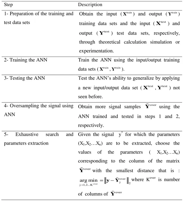
5.2 Parameter extraction based on ANN and exhaustive search 75 5.2.1 Preparation of the training and test data sets 75
5.2.2 Training the ANN algorithm 76 5.2.3 Testing the ANN algorithm 76
5.2.4 Oversampling of the signal using ANN 77
5.2.5 Parameter extraction through exhaustive search 77 5.3 Application to cathodoluminescence 79
5.3.2 Testing the algorithm 85
5.3.3 Oversampling of the CL signal 88 5.3.4 Exhaustive search 90
5.3.5 Effect of measurment noise 92 5.4 Application to EBIC 94
5.4.1 Training the ANN 95 5.4.2 Testing the algorithm 99 5.4.3 Oversampling of EBIC 102 5.4.4 Exhaustive search 105 5.5 Conclusion 106
Chapter references 107
Chapter 6 Semiconductor parameter extraction using artificial neural networks and inverse modeling 109
6.1 Introduction 109
6.2 Parameter extraction based on ANN and inverse modeling 110 6.2.1 Preparation of the training and test data sets 110
6.2.2 Training the ANN algorithm 111 6.2.3 Testing the ANN algorithm 111 6.3 Application to cathodoluminescence 112 6.3.1 Training the algorithm 112
6.3.2 Testing the algorithm 117 6.4 Application to EBIC 120
6.4.1 Training the algorithm 120 6.4.2 Testing the algorithm 124 6.5 Conclusion 126
Chapter references 127
Chapter 7 Semiconductor parameter extraction using genetic algorithms 129 7.1 Introduction 129
7.2 Parameter extraction using genetic algorithms 130 7.2.1 Initialize the parameters 130
7.2.2 Define the objective function 130 7.2.3 Apply the genetic algorithm 130 7.2.4 Extract the solution 131
7.3 Application to cathodoluminescence 133 Effect of the initial population size 138 7.4 Application to EBIC 139
Chapter references 143
Chapter 8 Conclusion and future work 144 8.1 Conclusion 144
8.2 Future work 145
Author publications 147 Appendix A 148
Figure 2.1: Schematic geometry of the initial steps of electron scatterings . 24 Figure 2.2: A schematic illustration of elastic and inelastic scattering of an incident electron with a sample's atom 25
Figure 2.3: Schematic diagram of signals generated due to electron beam interaction with bombarded specimen. 26
Figure 2.4: Monte Carlo simulation of the energy dissipation in a Silicon sample using the slowing down approximation of Bethe for various values of the incident energy beam. 30 Figure 2.5: Monte Carlo simulation showing the size of the interaction volume as a function of the energy beam (number of electrons is 250). 32
Figure 2.6: Monte Carlo simulation showing the size of the interaction volume as a function of the atomic number (number of electrons is 250 with initial energy of 15KeV). 32 Figure 2.7: Monte Carlo simulation showing the interaction volume as a function of the tilt angle (number of electrons is 250 with initial energy of 15KeV). 33
Figure 2.8: The three main approximations of the generation volume shape: (a) pear, (b) spherical, and (c) hemispherical. 33
Figure 2.9: Schematic illustration of intrinsic luminescence in direct (a) and indirect (b) semiconductors. 35
Figure 2.10: Schematic illustration of extrinsic luminescence: (1), (2) band-donor or acceptor, (3), (4) donor-acceptor. 35
Figure 2.11: Schematic illustration of the model employed for deriving CL signal. 36 Figure 2.12: CL signal calculated using the model of Hergert et al with a Wu and Wittry generation rate for a GaAs semiconductor: (a) dependence on diffusion length L, (b)
dependenceondeadlayerthicknessZt,and(c)dependenceonabsorpetioncoefficientα. 41 Figure 2.13: Different configurations used for EBIC measurements, the shades area represents the built-in potential: (a) and (c) are normal configurations, (b) and (d) are planar
configurations. 43
Figure 2.14: Normal collector configuration of a p-n junction, with x distance between the beam and the junction. 44
Figure 2.15: EBIC profiles for the region around the edges of a depletion layer located at 0.3μm:(a)differentvaluesofthediffusionlengthL(S=0),(b)differentvaluesofthesurface recombinationvelocity(L=3μm). 48
function, (c) Sigmoid function. 56
Figure 3.3: Feedforward network with a single layer. 58
Figure 3.4: Typical feedforward network with two hidden layers and an output layer. 58 Figure 3.5: ANN system identification. 63
Figure 3.6: ANN inverse modeling. 64
Figure 5.1: Training curve of the ANN (CL). 82
Figure 5.2: Percentage error between theoretical training CL signal and the training CL signal calculated by ANN. 83
Figure 5.3: Probability density function PDF(bars) and cumulative density function CDF (solid line) of the percentage error of the training set (CL). 84
Figure 5.4: Percentage error between the theoretical test CL signal and the test CL signal calculated by ANN. 86
Figure 5.5: PDF and CDF of the percentage error for the test set (CL). 87 Figure 5.6: Percentage error between the theoretical oversampled CL signal and the oversampled CL signal calculated by ANN. 90
Figure 5.7: PDF and CDF of the percentage error for the oversampled set (CL). 90 Figure 5.8:PDFandCDFofpercentageerroroftheparametersα,L,Zt,Q. 91
Figure 5.9:PDFandCDFofpercentageerroroftheparametersα,L,Zt,QwithaSNRof10 dB. 93
Figure 5.10: PDF and CDF of percentage erroroftheparametersα,L,Zt,QwithaSNRof20 dB. 93
Figure 5.11:PDFandCDFofpercentageerroroftheparametersα,L,Zt,QwithaSNRof30 dB. 94
Figure 5.12: Training curve of the ANN (EBIC). 96
Figure 5.13: Percentage error between theoretical training EBIC and the training EBIC calculated by ANN. 97
Figure 5.14: Probability density function PDF (bars) and cumulative density function CDF (solid line) of the percentage error for the training set (EBIC). 98
Figure 5.15: Percentage error between the theoretical test EBIC and the test EBIC calculated by ANN. 100
Figure 5.16: PDF and CDF of the percentage error for the test set (EBIC). 101
Figure 5.17: Percentage error between the theoretical oversampled EBIC and the oversampled EBIC calculated by ANN 103
Figure 5.18: PDF and CDF of the percentage error for the oversampled set (EBIC). 104 Figure 5.19: PDF and CDF of percentage error of the parameters L, S. 105
ANN for the training set (CL).. 115
Figure 6.3: Probability density function PDF (bars) and cumulative density function CDF (solidline)ofthepercentageerrorofL,α,S,Q,andZtforthetraining set 116
Figure 6.4: Percentage error between the theoretical parameters and the parameters calculated by ANN for the test set (CL). 118
Figure 6.5:PDFandCDFofthepercentageerrorofL,α,S,Q,andZtforthetestset. 119 Figure 6.6: Training curve of the ANN (EBIC) 122
Figure 6.7: Percentage error between theoretical training parameters and the parameters calculated by ANN (EBIC). 123
Figure 6.8: PDF (bars) and CDF (solid line) of the percentage error for the training set (EBIC). 123
Figure 6.9: Percentage error between the theoretical parameters and the parameters calculated by ANN for the test set (EBIC) 125
Figure 6.10: PDF and CDF of the percentage error of L, S of the test set 126
Figure 7.1: Flowchart of the proposed parameter extraction algorithm based on GA 132 Figure 7.2:CostsurfaceoftheobjectivefunctionofthetwoparametersLandα. 134
Figure 7.3: Convergence of the GA: (a) best and mean fitness, (b) average distance between individuals 135
Figure 7.4: PDF (bars) and CDF (solid line) of the percentage error for each of the parametersL,α,S,Q,andZt.. 137
Table 5.1: Summary of different steps of the parameter extraction algorithm based on ANN and exhaustive search 79
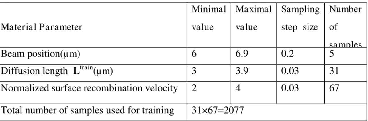
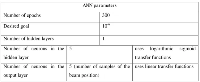
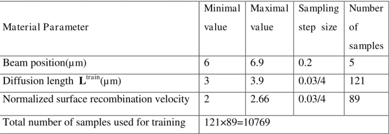
Table 5.2: Semiconductor parameters used for training (CL) 81 Table 5.3: ANN parameters used for training (CL) 82
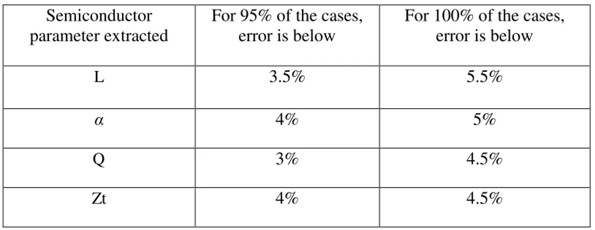
Table 5.4: Error for 95% and 100% of the training samples (CL) 84
Table 5.5: Semiconductor parameters used for testing the ANN (CL) 85 Table 5.6: Error for 95% and 100% of the test samples (CL) 87
Table 5.7: Semiconductor parameters used to obtain the oversampled CL signal 88 Table 5.8: Error for 95% and 100% of the oversampled samples (CL) 90
Table 5.9:Errorofthefourparametersα,L,Zt,Qfor95%and100%ofthecases 92 Table 5.10: Semiconductor parameters used for training (EBIC) 95
Table 5.11: ANN parameters used for training (EBIC) 96
Table 5.12: Error for 95% and 100% of the training samples (EBIC) 99 Table 5.13: Semiconductor parameters used for testing the ANN (EBIC) 99 Table 5.14: Error for 95% and 100% of the test samples (EBIC) 101
Table 5.15: Semiconductor parameters used to obtain the oversampled EBIC 102 Table 5.16: Error for 95% and 100% of the oversampled samples (EBIC) 104
Table 5.17: Error of the two parameters L, S for 95% and 100% of the cases (EBIC) 106 Table 6.1: Semiconductor parameters used for training (CL) 113
Table 6.2: ANN parameters used for training.(CL) 114
Table 6.3:PercentageerrorofthefiveparametersL,α,S,Q,andZtfor95%and100%ofthe training samples (CL) 117
Table 6.4: Semiconductor parameters used for testing the ANN (CL). 117
Table 6.5: Percentage error of thefiveparametersL,α,S,Q,Ztfor95%and100%ofthetest samples . 119
Table 6.6: Semiconductor parameters used for training (EBIC). 121 Table 6.7: ANN parameters used for training (EBIC). 121
Table 6.8: percentage error of the two parameters for 95% and 100% of the samples (EBIC). 124
Table 6.9: Semiconductor parameters used for testing the ANN (EBIC). 124
Table 6.10: Percentage error of the two parameters L and S for 95% and 100% of the samples. 126
Table 7.3:MaximumpercentageerrorofthefiveparametersL,α,S,Q,andZtfor95%and 100% of the runs, respectively 137
Table 7.4:MaximumpercentageerrorofthefiveparametersL,α,S, Q, and Zt for 95% and 100% of the runs, respectively, with different initial population size 139
Table 7.5: Lower and upper bounds of semiconductor parameters (EBIC) 140 Table 7.6: GA parameters (EBIC) 140
Table 7.1: Maximum percentage error of the two parameters L and S for 95% and 100% of the runs, respectively 141
Chapter 1
Introduction
Contents
1.1 Background ... 1.2 Aim of this work ... 1.3 Thesis organization ... 1.4 Thesis contributions ... chapter references ...
1.1
Background
The investigation of electronic and optical properties of semiconductors is of fundamental importance as the performance of electronic devices is dictated by the properties of the carriers inside the materials. The scanning electron microscopy has proven to be an effective, useful and nondestructive technique in the characterization of semiconductor materials. In scanning electron microscopy, Electron Beam Induced current (EBIC) and Cathodoluminescence (CL) have been extensively used as an analytical tool in the characterization of semiconductor materials. They have been widely used for the investigation of crystal defects in semiconductors [1-7] and for the extraction of defect free region semiconductor parameters such as: absorption coefficient (α), diffusion length (L), dead layer thickness (Zt), relative quantum efficiency (Q) and the normalized surface recombination velocity (S) [8-14]. The
extraction of these parameters is difficult because of there nonlinear and complex effect on the CL/EBIC signal, and the high interaction between theme.
The parameter extraction problem is a multi-minimum optimization problem [15,16] and it can be solved using several optimization techniques, which can be roughly classified into two categories: deterministic optimization algorithms (pseudo-objective function substitution method (POSM)[17], Levenberg-Marquardt [18], the gradient descent methods [19],… ) and stochastic optimization algorithms ( simulated annealing method (SA) [20], simulated 1-diffusion method (SD)[21], genetic algorithms (GA) [22, 23]…). These methods were applied to parameter extraction of semiconductor devices and integrated circuits [22-32].
Optimization algorithms tend to adjust the inputs such that the cost function, also known as the objective function, is either minimized or maximized (depending whether it is a minimization or a maximization problem). One of the largest problems in optimization is to determine whether the solution found is a global solution
(corresponds to finding the global minimum/maximum) or a suboptimum solution
(corresponds to finding the local minimum/maximum).
The parameter extraction can be described as an optimization problem as follows: suppose that a process f has an output y which is a function of a set of parameters x, that is: y = f(x). Given a process output measurement y′, the parameter extraction problem is equivalent to minimizing the error function E(x) with respect to the process parameters x, subject to a set of constraints C. The error function E(x) is a general error function between y′ and f(x), that is: E(x) = E(y′-f(x)) and it represents the objective function to be minimized. The optimization process determines the set of parameters x* that minimizes the objective function E(x) subject to the set of constraints C (i.e. the upper and lower bounds on parameters), that is:
subject to arg min ( ( ))E x C x x (1-1)
1.2
Aim of this work
The aim of this work is to extract the defect free region semiconductor parameters from the EBIC/CL signals using advanced signal processing techniques. Particularly, we are interested in the simultaneous extraction of related semiconductor parameters (α, L, S, Zt, Q) from any EBIC/CL; our novel approaches are based on powerful modeling and optimization techniques: Artificial Neural Networks and Genetic Algorithms. To the best of our knowledge, no work has been reported in this regard.
Artificial neural networks have many desirable properties such as: their ability to learn by example through training, their ability to generalize and predict, and finally their inherent parallel computation capability. These, characteristics suggest that they can be used for modeling of complex systems and processes and consequently motivated us to employ them for the modeling of the EBIC/CL signal generation process.
At the other hand, by being able to formulate the semiconductor parameter extraction problem as an optimization problem, suggests that powerful optimization techniques can be used to find near-optimum solutions with reasonable cost. This motivated us to explore the feasibility of using evolutionary optimization algorithms that exhibit many desirable properties such as, their moderate computational complexity and their excellent performance. Because genetic algorithms are the most popular evolutionary algorithms, we use them here for semiconductor parameter extraction.
1.3
Thesis organization
The dissertation is divided into the following chapters:
Chapter 1 gives a brief background about the semiconductor parameter extraction problem, describes the aim of the dissertation and its major contributions to the literature.
Chapter 2 talks about the fundamentals of CL and EBIC in the Scanning Electron Microscopy. The chapter also describes the Monte Carlo simulation of the electron beam interactions with the semiconductor material. Additionally, MATLAB related codes are reported in the Appendix.
Chapter 3 contains fundamentals of Artificial Neural Networks. Chapter4 contains fundamentals of Genetic Algorithms.
In chapter5 a new approach based on feedforward ANN and exhaustive search for the simultaneous extraction of related semiconductor parameters is developed.
In chapter6 a new approach for the simultaneous extraction of related semiconductor parameters based on feedforward ANN and inverse modeling is developed and described.
In chapter7 a new approach for the simultaneous extraction of related semiconductor parameters based on genetic algorithms is developed.
Chapter 8 consists of a conclusion that summarizes the results and the contributions of the dissertation, and discusses some recommendations for future work.
1.4
Thesis contributions
The major contribution of this work resides in the introduction of new signal processing techniques to the field of scanning electron microscopy which opens the door widely to the use of these techniques in other related fields. The main contributions of the dissertation are summarized into the following points:
Development of a new approach that is based on ANN and exhaustive search for the simultaneous extraction of related semiconductor parameters. Development of a new approach that is based on ANN and inverse modeling
for the simultaneous extraction of related semiconductor parameters.
Development of a new approach that makes use of Genetic Algorithms for the simultaneous extraction of related semiconductor parameters.
Chapter references
1- H, J, Leamy, "Charge collection scanning electron microscopy". J.Appl.Phys, 53(6). pp. R51-R80. 1982
2- C, Donolato. "On the theory of SEM charge collection imaging of localized defects in semiconductors". Optik 52No. 1. 19-36. 1978
3- A, Jackubowicz. "On the theory of electron beam induced current contrast from pointlike defects in semiconductors". J. Appl.Phys, 57(4), pp. 1194-1199, 15. 1985
4- A, Jackubowicz. "Theory of cathodoluminescence contrast from localized defects in semiconductors". J. Appl.Phys. 59(6). pp. 2205-2209. 15. 1986
5- A, Jakubowicz. "Theory of lifetime measurement with the scanning electron microscope in a semiconductor containing a localized defect: transient analysis". J. Appl.Phys. 58(4). pp 1483-1488. 1985
6- K, L, Pey. D,S,H, Chan. and J,C,H, Phang. "Cathodoluminescence contrast of localized defects part1. Numerical model for simulation, part2. defect investigation", Scanning Mmicroscopy. Vol. 9, pp. 355-380, No. 2. 1995 7- S, Hildebrandt. J, Schreiber. W, Hergert. H, Uniewsk. and H, S, Leipner.
"Theoritical fundamentals and experimental materials and defect studies using quantitative scanning electron microscopy-cathodoluminescence/electron beam induced current on compound semiconductors". Scanning microscopy. Vol. 12, No. 4 (pages 535-552). 1998
8- H, C, Casey. Jr, D, D, Sell. and K, W, Wecht "concentration dependence of the absorption coefficient for n-and p-type GaAs between 1.3 and 1.6 eV". Journal of applied physics, Vol. 46, No1. 1975
9- V, K, S, Ong. "A direct method of extracting surface recombination velocity from an electron beam induced current line scan. Review of scientific instruments", Vol. 69, No. 4. 1998
10- W, Hergert. P, Reck. L, Pasemann. And J, Schreiber "Cathodoluminescence measurements using the scanning electron microscope for the determination of semiconductor parameters". Phys. Stat. Sol. (a)101, 611. 1987
11- F, Koch. W, Hergert. G, Oelgart. and N, Puhlmann "determination of semiconductor parameters by electron beam induced current and cathodoluminescence measurements". phys. Stat. Sol. (a)109,261. 1989 12- S, Hildebrandt. J, Schreiber. W, Hergert. and V, I, Petrov, "Determination of
1-xPx (x=0.375, 0.78) from beam voltage dependent measurements of cathodoluminescence spectra in the scanning electron microscope". Phys. Stat. Sol. (a)110, 283. 1989
13- N, Puhlmann. G, Oelgart, "Semiconductor Characterization by means of EBIC, Cathodoluminescence, and photoluminescence". Phys. Stat. Sol. (a) 122,705. 1990
14- D, S, H, Chan. K, L, Pey. and J, C, H, Phang (1993) Semiconductor parameter extraction using cathodoluminescence in the scanning electron microscope. IEEE transactions on electron devices. Vol. 40. No. 8.
15- A, K, Hartmann. H, Rieger, "Optimization algorithms in Physics". Wiley-VCH Verlag Berlin GmbH. Berlin (Federal Republic of Germany) 1st edition. 2002.
16- R, L, Haupt. and S, E, Haupt, "Practical Genetic Algorithms". 2nd edituion. Jhon Wiley and Sons. INC. publications. New Jersey. 2004.
17- G, L, Tan. S, W, Pan. W, H, Ku. and A, J, Shey, "ADIC-2.C: A General-Purpose Optimization program Suitable for Integrated Circuit Design Applications Using the Pseudo Objective Function Substitution Method (POSM)". IEEE Transactions on computer aided design. Vol. 1. No. 11. pp. 1150-1163. 1988.
18- M, I, Lourakis. A, A, Argyros, "Is Levenberg-Marquardt the most efficient optimization algorithm for implementing bundle adjustment". Proceeding of the Tenth IEEE international conference on computer vision. Vol. 2, pp. 1526-1531. 2005.
19- S, Haykin, "Neural Networks; A Comprehensive Foundation". Prentice Hall, 2 edition. 1999
20- D, Bertsimas. and J, Tsitsiklis, "Simulated Annealing. Statistical Science". Vol. 8. No. 1. 10-15. 1993
21- T, Sakurai. B, Lin. and A, R, Newton, "Fast Simulated Diffusion: An Optimization Algorithm for Multiminimum Problems and Its Application to MOSFET Model Parameter Extraction". IEEE Transactions on computer aided design. Vol 11. No 2. pp. 228-234. 1992
22- G, Antoun. El-Nozahi, M. Fikry, W. Abbas, H. "A hybrid genetic algorithm for MOSFET parameter extraction". IEEE Canadian Conference on Electrical and Computer Engineering. 4-7 . vol.2. pp: 1111- 1114. 2003
23- Y, Li. "An automatic parameter extraction technique for advanced CMOS device modeling using genetic algorithm". Microelectronic Engineering. 84. 260–272. 2007
24- Y, S, Yu, "Parameter Extraction of Si-Based Single-Electron Transistor with Electrical Tunnel Barriers for Circuit Simulation". Journal of the Korean Physical Society. Vol. 47. pp. S547-S551. 2005
25- C, Scharff. J, C, Carter. and A, G, R, Evans, "New and fast MOSFET parameter extraction method". Electronics letters. Vol. 28 No. 21 pp. a2006-2008. 1992
26- P, R, Karlsson. K, O, Jeppson, "An efficient parameter extraction algorithm for MOS transistor models". IEEE Transaction on Electron Devices. Vol. 39. No. 9 2070-2076. 1992
27- Y, Hao. L, A, Yang. C, L, Yu, "An optimization technique for parameter extraction of ultra_deep submicron LDD MOSFET’s". Solid State Electronics 50.1540-1545. 2006
28- D, Busuioc, "Circuit model parameter extraction and optimization for microwave filters. Master thesis. University of waterloo". Ontario Canada. 2002.
29- H, Wang. H, Z, Yang. and G, Z, Hu, "Combinatorial Algorithms for BJT Model Parameters Extraction". ICSE’96 Proc. pp. 144-147. Penang, Malaysia. 1996.
30- K, Garwacki, "Extraction of BJT model parameters using optimization method". IEEE transactions on computer-aided design. Vol. 7. No. 8. pp. 850-854. 1998.
31- B, Liu. J, Lu. Y, Wang. and Y, Tang, "An effective parameter extraction method based on memetic differential evolution algorithm". Microelectronics Journal. Volume 39. Issue 12.. Pages 1761-1769. 2008.
32- R, A, Thakker. M, B, Patil. K, G, Anil, "Parameter extraction for PSP MOSFET model using hierarchical particle swarm optimization". Engineering Applications of Artificial Intelligence. Volume 22. Issue 2. Pages 317-328. 2009.
Chapter 2
Scanning Electron Microscopy Fundamentals
Contents
2.1 Introduction ... 2.2 Interaction of the incident electrons with irradiatted sample ... 2.3 Cathodoluminescence CL ... 2.4 Electron Beam Induced Current ... Chapter references ...
2.1 Introduction
The Electron Microscopy [1,2,3,4] was developed due to the limitations of
light microscopy [5], it has been an important tool for the study and analysis of different specimens, it permits the observation and characterization on a nanometer to
micrometer scale.
The Scanning electron microscopy SEM [1,2,3,4] is a type of Electron Microscopy, it
is one of the most widely used techniques in research and industry. Basically a beam of highly accelerated electrons that typically has an energy ranging from 0.5 KeV to 50 KeV bombard a sample to be examined; When they penetrate into the sample they undergo interaction processes (figure2-1) that may result in the loss of energy, change of direction, and the creation of secondary signals (electron signals or photon signals).
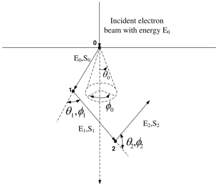
Incident electron beam with energy E0
0 0
1,
1
2,
2
0 1 2 E0,S0 E1,S1 E2,S2Figure 2-1. Schematic geometry of the initial steps of electron scatterings.
2.2 Interaction of the incident electrons with the irradiated matter
2.2.1 Physical process
Generally, the interaction processes that undergo the incident electrons can be grouped in two types [6]:
Elastic: in which only the trajectory of the incident electron changes while the kinetic energy and velocity remain constants. Elastic scattering results from the deflection of the incident electron by the positive charge of the nucleus of the atoms of the sample. It gives rise to high energy backscattered electrons. The cross section for elastic scattering obeys an inverse square dependence with the electron beam energy, and a squared proportional with the atomic number of the sample.
Inelastic: in which the incident electron lose significant and definite amount of energy, inelastic process occurs during the interactions of the incident electron with the electrons and atoms of the sample.
A schematic illustration of the elastic and inelastic interactions is illustrated in figure2-2. elastique
inelastique
Elastic scattering Inelastic scattering Generated signalFigure2-2. A schematic illustration of elastic and inelastic scattering of an incident electron with a sample's atom.
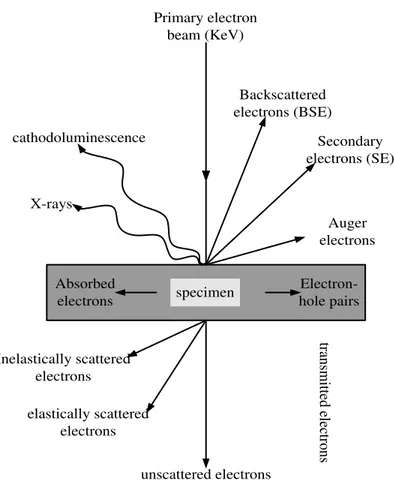
As a consequence of the inelastic interactions a wide range of secondary signals are produced, Figure2-3 illustrates these signals (The directions shown doesn't represent the physical direction of the signal).
Primary electron beam (KeV) Backscattered electrons (BSE) Secondary electrons (SE) Auger electrons cathodoluminescence X-rays Inelastically scattered electrons elastically scattered electrons unscattered electrons tra ns m itt ed e le ct rons Electron-hole pairs Absorbed electrons specimen
Figure 2-3. Schematic diagram of signals generated due to electron beam interaction with bombarded specimen.
2.2.2 Function of energy dissipation
Constantly the inelastic processes reduce the energy of a primary electron, finally to the point at which it is "captured". It is useful to study the energy loss of the incident electrons quantitatively as a function of the distance traveled and also the target composition (atomic number Z, atomic weight A, and density ρ). Bethe in 1933 derived the continuous energy loss approximation for all inelastic processes, the energy loss per unit of distance traveled by the incident electron dE/ds (the electron beam suffers a mean energy loss dE in penetrating a distance ds) is given by [7, 8]:
4 2 ( ) ln dE e aE eV NZ ds E J (2-1)
where E is the kinetic energy of the electrons, e is the electron charge, N is the number of atom's/cm3, and Z is the atomic number of the sample. Bethe gave for the constant a=2, J is a function of the atomic number and is given by [7, 8]:
( ) 11.5
J eV Z (2-2)
(2-2) can be expressed as follows:
4 2 2 ( ) ln 11.5 dE e E eV NZ ds E Z (2-3)
It is suitable to express the energy loss in the unit of KeV/ m, and in terms of the
atomic weight and density of the target material, (2-3) becomes [7, 8]: 174 7.83 ln dE Z E KeV ds AE Z m (2-4)
where, ρ(g/cm3) is the sample density, and A(g) is the atomic weight of the sample.
2.2.3 Electron range
As a result of the elastic and inelastic scatterings that the incident electrons undergo within the material, the original trajectories are randomized. The distance traveled between the point of entry and the final resting place of an incident electron undergoing inelastic scatterings is the Bethe range RB, it is defined from the Bethe
equation as follows [8,9]:
00 1 / B E R cm dE dE dS
(2-5)(2-5) overestimates the electron range because it neglects the effect of elastic scatterings. The effective depth to which energy dissipation extends is much smaller and it is known as Gruenrange or penetration range Re, it is a function of
the primary energy beam E0 and it is given by this general formula [10]:
0
( / )
R K E (2-6)
where ρ is the material density in g/cm3, K and α depends on the atomic number and E0. Everhart and Hoff, for example, proposed for K, α and R the values [10]:
1.75 0
( ) (0.0398 / )
R m E (2-7)
where E0 is in KeV.
Whereas kanaya and Okayam proposed the following expression [10]:
0.889 1.67 0
( ) (0.0276 / )
R m A Z E (2-8)
where A is the atomic weight in (g/mol), Z is the atomic number, and E0 is in
KeV.
2.2.4 Generation of pairs
The generation of electrons-holes pairs is an inelastic process escorting the penetration of electrons inside the semiconductor sample; we can define a function
,G r R describing the distribution of generated pairs in the volume. It corresponds to
the number of generated pairs per unit volume and unit time (cm-3.s-1) in the point spotted by the vectorr x y z( , , ). The parameter R here indicates the dependence on the energy beam.
Virtually, we don’t need to know the explicit form of the function G but only its projection on a plan. If the projection of G on the plan (xy), for example, is g(z) it
corresponds to the number of pairs generated per unit depth per unit time. It is given by the following formula [8,11] :
0 ( ) e h I dE g z qE dz (2-9)
where I0 is the incident electron beam current, q is electronic charge, Ee-h is the
mean energy required to create an electron-hole pair, and dE is the mean energy loss per depth dz.
If we normalize the mean energy loss to the energy beam, and the depth to the electron range we can define the depth-dose function as follows:
0 ( / ) ( / ) ( / ) d E E z R d z R (2-10)
The depth-dose function represents the number of electron-hole pairs generated
per electron of energy E per unit depth per unit time Equation (2-9) becomes: 0 0 ( ) ( / ) e h I E g z z R qE R (2-11)
In figure2-4 we reported the variation of the energy dissipation with the depth for different values of the incident energy beam using a Monte Carlo simulation (the code is detailed in Appendix A) in a silicon sample.
0 0.5 1 1.5 2 2.5 3 0 2 4 6 8 10 12 14 Z(μm) En e rg y d issi p a ti o n Eb=10KeV Eb=15KeV Eb=20KeV
Figure2-4. Monte Carlo simulation of the energy dissipation in a Silicon sample using the slowing down approximation of Bethe for various values of the incident energy
beam.
The choice of the generation function is important to get a good accuracy for semiconductor parameter measurements. Various analytical generation functions have been published; the most famous are:
Everhart and Hoff have proposed for the depth-dose function a polynomial expression [10,12]:
2 3
( /z R) 0.60 6.21( /z R) 12.40( /z R) 5.69( /z R)
(2-12)
It is the most used because of its simplicity. Wittry proposed a Gaussian function [13]
2 0 / ( /z R) Aexp z R u u (2-13)
Kyser proposed a modified Gaussian function [14]:
2 0 0 ( / ) ( / ) ( /z R) Aexp z R u Bexp b z R u u (2-14)
where, A, u0, Δu, B, b are constants.
The number of pairs created in the sample per unit time is the total generation
rate G0(s -1 ) [8]: 0 0 ( ) G
g z dz (2-15) 2.2.5 Generation volumeThe generation volume or interaction volume is the 3-dimentional space in which
primary incident electrons have enough energy to interact with the specimen. Its shape and its size are controlled by both elastic and inelastic interactions: if elastic
scatterings are the dominant interaction, electrons tend to scatter away from their
original direction which gives "width" for the interaction volume. However if
inelastic scatterings are the dominant interactions, electrons are less deviated; they
penetrate into the sample along their original trajectories and lose energy as they penetrate.
The two factors that can determine which interactions, elastic or inelastic, can dominate are the primary energy beam and the atomic number of the sample.
As the primary energy beam increases, the incident electrons penetrate into the sample along a path close to their incident direction, as they lose energy by inelastic scatterings the probability of elastic scatterings increase so they begin deflected into
the sample. Figure2-5 shows a Monte Carlo simulation (see Appendix A for the MATLAB code) of the generation volume as a function of the energy beam.
-1.5 -1 -0.5 0 0.5 1 1.5 0 0.2 0.4 0.6 0.8 1 1.2 1.4 1.6 1.8 2 -1.5 -1 -0.5 0 0.5 1 1.5 0 0.2 0.4 0.6 0.8 1 1.2 1.4 1.6 1.8 2 -1.5 -1 -0.5 0 0.5 1 1.5 0 0.2 0.4 0.6 0.8 1 1.2 1.4 1.6 1.8 2
5KeV 10 KeV 20 KeV
figure2-5. Monte Carlo simulation showing the size of the interaction volume as a function of the energy beam (number of electrons is 250).
Electrons entering a high atomic number sample are scattered away from their original directions. However in a low atomic number sample electrons penetrate into the sample and can lose energy by inelastic scatterings till their energy is such that the elastic scatterings can dominate. Figure2-6 shows a Monte Carlo simulation (see Appendix A for MATLAB codes) of the generation volume as a function of the atomic number of the target.
-2 -1.5 -1 -0.5 0 0.5 1 1.5 2 0 0.5 1 1.5 2 2.5 -2 -1.5 -1 -0.5 0 0.5 1 1.5 2 0 0.5 1 1.5 2 2.5 -2 -1.5 -1 -0.5 0 0.5 1 1.5 2 0 0.5 1 1.5 2 2.5 Si (Z=14) Ge (Z=32) Ag (Z=47)
figure2-6: Monte Carlo simulation showing the size of the interaction volume as a function of the atomic number (number of electrons is 250 with initial energy of
The tilt angle, which is the angle between the sample surface and the horizontal plane, determines the symmetry of the interaction volume; as the sample is tilted away from the horizontal the interaction volume appears asymmetric. Figure2-7 shows a Monte Carlo simulation (see Appendix A for MATLAB codes) of the generation volume as a function of tilt angle.
-0.8 -0.6 -0.4 -0.2 0 0.2 0.4 0.6 0.8 1 1.2 0 0.2 0.4 0.6 0.8 1 1.2 -0.6 -0.4 -0.2 0 0.2 0.4 0.6 0.8 1 -0.1 0 0.1 0.2 0.3 0.4 0.5 0.6 0.7 0.8 0.9 -0.4 -0.2 0 0.2 0.4 0.6 0.8 1 -0.1 0 0.1 0.2 0.3 0.4 0.5 0.6 0.7 0.8 Normal
incidence Tilt angle=30 0
Tilt angle=550
figure2-7. Monte Carlo simulation showing the interaction volume as a function of the tilt angle (number of electrons is 250 with initial energy of 15KeV).
From figure2-5,2-6 and 2-7 we can see that the boundaries of the generation
volume can not be well defined but only approximated. Generally the shape of the
generation volume is approximated to one of three main shapes: pear, spherical, or hemispherical shape (figure2-8).
Electron beam Electron beam Electron beam (a) (b) (c)
Figure2-8. The three main approximations of the generation volume shape: (a) pear, (b) spherical, and (c) hemispherical.
2.3 Cathodoluminescence (CL)
The cathodoluminescence (CL) analysis permits the evaluation of different properties of materials. For example; the CL spectroscopy can be used in the identification and measurement of luminescent center concentrations and distribution, the dependence of CL intensity on electron beam voltage is used to determine electronic properties (carrier diffusion length, surface recombination velocity…), CL maps can be used to find the concentration and distribution of defects (dislocations…).
2.3.1 Physical phenomena
The cathodoluminescence is the emission of photons from a solid supplied with
electron excitation or cathode rays. As mentioned earlier, the inelastic processes occurring during the penetration of the incident energetic electrons in the bombarded sample generate electron-hole pairs, the excess carriers diffuse inside the material and recombine, either by radiative or nonradiative processes.
The radiative recombination may be an intrinsic or extrinsic mechanism [10,15,16] :
Intrinsic luminescence results from the recombination of electrons and holes across the fundamental energy gap; it is an intrinsic property of the material. In indirect gap semiconductors the recombination must be accompanied by the simultaneous emission of a photon and a phonon to conserve the momentum. A schematic illustration of the intrinsic luminescence in direct and indirect semiconductors is presented in Figure2-9.
Conduction band Conduction band valenc e band valenc e band gap Energ y level gap Energ y level hnj=Efinal
-Einitial hnj=Efinal-Einitial
-Ephonon
Wave vector K Wave vector K
(a) (b)
Figure2-9 –Schematic illustration of intrinsic luminescence in direct (a) and indirect (b) semiconductors.
Extrinsic luminescence results from the radiative transitions involving shallow or deep energy states located within the forbidden band gap in both direct and indirect semiconductors. A schematic illustration of the extrinsic emission is reported in figure2-10. ga p Valence band conduction band Donors level Acceptor s level (4 ) (3 ) (2 ) (1 )
Figure2-10 –Schematic illustration of extrinsic luminescence: (1), (2) band-donor or acceptor, (3), (4) donor-acceptor.
2.3.2 Formation of the CL signal
Let us consider a semi infinite homogenous n-type semiconductor, bounded by the top surface (figure2-11), having minority carrier (holes) diffusion coefficient and life time Dp and , respectively, and surface recombination velocity vs. bombarded on
the top surface by an electron beam of energy E0.
Electron beam E0 (KeV)
g(r) Generation volume surface semiconductor x z
v
sD
p,
Figure2-11. Schematic illustration of the model employed for deriving CL signal.
The generation of photons is essentially governed by the stationary excess minority carriers concentration p(r); which in the steady state obeys the differential equation given by [16,17,18]: 2 ( ) ( ) ( ) 0 p p r D p r g r (2-16) where, g(r) is the generation rate per unit volume and unit time.
With the boundary condition at the top surface, that takes into account the surface recombination:
( ) ( ) p s dp r D v p r dz (2-17)
The generation of photons is essentially governed by the stationary excess minority carriers’ concentration p(r).
( ) CL r V p r I dV
(2-18) After radiative recombination occurs the emitted photons propagate inside the semiconductor, due to optical absorption and reflection losses not all generated photons are emitted; only a fraction of them is coming out from the material. Thus the total CL intensity; which is the number of photons emitted per unit time; is given by [10, 19, 20]: ( ) ( ) CL r V p r I F z dV
(2-19) where, r is the radiative recombination lifetime of the minority carriers, and F is thecorrection function for optical absorption and reflection losses.
2.3.3 Calculation of the CL signal using Hergert et al model
Many models were proposed for the calculation of the cathodoluminescence signal, using analytical approach [10, 20, 21, 22] or using Monte Carlo simulation [25]. We choose the model of Hergert et al [22-23-24] because of its simplicity. The details of that model are given now.
In this model the equation (2-19); which is the current of photons modified by the internal absorption of the luminescence radiation; is written as follows:
/ cos 0 ( ) 2 sin c z CL r V p r I d e dV
(2-20) where θc is the critical angle of the total reflection, and α is the absorptioncoefficient of the semiconductor.
The minority carrier density in (2-20) is obtained from the continuity equation in cylindrical coordinates: 2 2 2 1 1 1 ( , ) p p r p g r z r r r z L D (2-21)
The boundary conditions for the geometry of semi infinite semiconductor of figure2-11 are as follows:
0 ( 0) p s z p D p z z (2-22-a) ( ) 0 p z (2-22-b)
The electron-hole pairs due to absorption of internal luminescence are not taken into account.
To solve (2-21) a Hankel transform of order 0 is used; the Hankel transform and the inverse Hankel transform of minority carrier density are given by:
0 0 ( , ) ( , ) ( ) p z p r z J r rdr
(2-23-a) 0 0 ( , ) ( , ) ( ) p r z p z J r d
(2-23-b) where, J0is the Bessel function of first kind of order 0.This gives the following equation: 2 2 2 2 1 1 ( , ) ( , ) ( , ) d p z p z g z dz L D (2-24)
(2-24) is soled using Green's function, which leads to:
0 1 ( , ) ( , , ) ( , ) 4 p z G z z g z D
(2-25) where G(z,z', ) is the Greens function of (2-24).with: 0 0 1 ( ) ( ) rdrJ r
(2-26) where δ is the Dirac delta function.Equation (2-20) becomes as follows:
/ cos 0 0 0 sin ( , , 0) (0, ) c z CL r I d dz G z z g z e dz D
(2-27) The CL signal was then expressed by a universal function which depends only on the depth distribution g(z) as follows:1 1 0 ( ,x z ) e xzg z( z dz)
(2-28) and the CL signal is then given by:0 2 ˆ sin ( ) CL r I d F
(2-28) with: ˆ / cos (2-29-a)0 2 2 1 ( ) ( , ) , (1 ) 1 xZt G e Lx S F x x Zt Zt x L S L (2-29-b) where:
G0 is the total generation rate of the minority carriers.
nr r/( nr r) is the total life time with nr and r are the non radiative
and radiative life time of the semiconductor, respectively. L is the diffusion length of the excess minority carriers. g is the depth distribution function of the generation rate. Z is the distance from the surface.
S is the normalized surface recombination velocity given by: S= Vs/Vd. where Vs is the surface recombination velocity and Vd is the diffusion velocity given by: Vd=L/ .
The depth distribution of the energy dissipation is of Wu and Wittry, it is the modified Gaussian approximation of Kyser[14] reported in (2-14). It can be written as: 2 0 0 ( )u Aexp u u Bexp bu u u (2-30)
where: u=ρZ/R , ρ(g/cm3) is the density of the semiconductor material and Z is the depth.
The electron range R is:
3 1.7 0 2.56 10 ( ) ( ( ) / 30) R cm E KeV (2-31) For GaAs: u0=0.125, Δu=0.350, b=4, and B/A=0.4, the atomic number is 32,
and the critical angle is 160. Figure2-12 illustrates CL signals calculated using the approach described before.
0 5 10 15 20 25 30 35 40 0 0.5 1 1.5 2 2.5 3
energy beam KeV
C L s ig n a l (a rb it ra ry u n it s) ( a ) L=2µm L=4µm L=0.5µm L=1µm =0.1µm-1 Zt=0µm S=infinity 0 5 10 15 20 25 30 35 40 0 0.5 1 1.5 2 2.5 3
energy beam (KeV)
C L s ig n a l (a rb it ra ry u n it s) (b) Zt=1µm Zt=0.1µm Zt=0.5µm Zt=0µm L=1µm =0.1µm-1 S=infinity 0 5 10 15 20 25 30 35 40 0 0.5 1 1.5 2 2.5 3
energy beam KeV
C L s ig n a l (a rb it ra ry u n it s) =0.5µm-1 =0.1µm-1 =0.01µm-1=0µm-1 L=1µm Zt=0µm S=infinity (d)
Figure2-12. CL signal calculated using the model of Hergert et al with a Wu and Wittry generation rate for a GaAs semiconductor: (a) dependence on diffusion length L, (b) dependence on dead layer thickness Zt, and (c) dependence on absorpetion coefficient α.
2.4 Electron beam induced current EBIC
The electron beam induced current (EBIC) technique allows examining semiconductor materials and looking for features such as crystallographic defects, as well as giving information about the semiconductor parameters that characterize the material such as the diffusion length and the surface recombination velocity.
2.4.1 Physical phenomena
As mentioned earlier, the inelastic processes occurring during the penetration of the incident energetic electrons in the bombarded sample generate electron-hole pairs, the excess carriers diffuse inside the material, when the semiconductor sample contains internal electric field (p-n junction or Schottky junction) the charge carriers are separated by that field and minority carriers can therefore reach the junction by diffusion this results in a charge-collection current or electron beam induced current EBIC, which can be amplified and measured externally when an external circuit is connected to the ends of the junction.
The EBIC can be performed in one of two modes:
Planar configuration in which the junction (p-n junction or Schottky junction) is perpendicular to the electron beam.
Cross sectional or normal configuration in which the junction (p-n junction or Schottky junction) is parallel to the electron beam.
w w w w Electron beam E0 Electron beam E0 Electron beam E0 Electron beam E0 I I I I x z (a) (a) (d) (c) (b)
Figire13. Different configurations used for EBIC measurements, the shades area represents the built-in potential: (a) and (c) are normal configurations, (b) and (d) are
planar configurations.
2.4.2 Calculation of the EBIC current in a normal-collector p-n junction
configuration
One of the most used configurations is the normal p-n configuration, the electron beam scanned over the surface and the steady state EBIC is measured as a function of the distance xb between the junction and the beam position (figure2-14.).
x z
Initial electron beam
with initial energy E0
Generatio n volume n-type semiconductor p-type semiconductor I xb
Figure2-14. Normal collector configuration of a p-n junction, with x distance between the beam and the junction.
2.4.2.1 The charge collection probability of Donolato
The model of Donolato [27] for the charge collection probability which is the EBIC due to a point source is detailed in this section.
In this model the presence of the back surface of the diode is neglected (sample thickness considered infinite) and the transport of the minority carriers generated by the electron beam in the neutral material (n type) is described by the steady state diffusion equation (2-16) [27].
According to [27], the configuration of figure2-14 has translational invariance along the y axis, in the sense that the contribution to the collected current of any source element doesn’t depend on its y coordinate. Thus the collected current depends only on the projected generation on the xz plane:
( , ) ( , , ) g x z g x y z dy
(2-32)Equation (2-16) becomes: 2 ( , ) ( , ) ( , ) 0 p p x z D p x z g x z (2-33)
The boundary conditions on the surface and at the junction plane are:
0 at 0 . at 0 p x p S p z z (2-34-a) (2-34-b) with S the normalized surface recombination velocity.
The solution of (2-33) is then:
0 0 ( , ) ( , ) ( , , , ) p x z dx g x z G x x z z dz
(2-35)where G(x,x',z,z') is the Green's function for equation (2-33) satisfying the boundary conditions (2-34).
The charge collection probability i(x',z') at a point (x',z') is :
0 0 ( ', ') G |x i x z D dz x
(2-36)Finally Donolato calculated the charge collection probability as follows:
2 0
2
( , ) exp( ) exp( ) sin( )
( ) S k i x z x z kx dk S
(2-37)where =1/L , L is the diffusion length of minority carriers, k is a constant, and
=(k2+ 2
)1/2.
For more details about calculation of (2-37) the reader is referred to [27].
2.4.2.2 Calculation of the EBIC current
The approach proposed in [28,29] is used for the calculation of the EBIC profiles:
First, the current is divided into three regions as proposed by Czaja [28]: the n-region, the depletion n-region, and the p-region. In each region the current is a convolution of the generation volume distribution g(x,z) and the charge collection probability i(x,z) with the assumption that the charge collection within the depletion region is unity. The EBIC current when the beam is located at a point x' is then given by: 0 0 0 ( ) ( , ) ( , ) ( , ) ( , ) ( , ) p n n p x x x x I x g x x z i x z dxdz g x x z dxdz g x x z i x z dxdz
(2-38)where: xn and xp are the edges location of the depletion region and the x axis in
(2-37) starts from the depletion region edge.
Then, a generation volume distribution proposed by Donolato is used to calculate the EBIC profiles, it is given by [28,29,30]:
2 2 2 ( / ) ( ) exp 2 , 2 ( , ) z R r g r R z R z R (2-39) where:R is the electron range related to the energy beam as follows:
1.75 2 0 ( ) ( ) 4 10 E KeV R m (2-40) ρ(g/cm3
) is the density of the sample. 2
is the standard deviation of the Gaussian distribution given by:
2 2 3
( ,z R) 0.36d 0.11z /R
(2-41)
( /z R)is the depth distribution, it follows the polynomial of Everhart and Hoff: 2 3 0.6 6.21( / ) 12.4( / ) 5.69( / ) 0 / 1.1 ( / ) 0 / 1.1 z R z R z R z R z R z R (2-42)
According to (2-32) the equation (2-39) becomes:
2 2 ( / ) ( , ) exp 2 2 z R x g x z R (2-42)
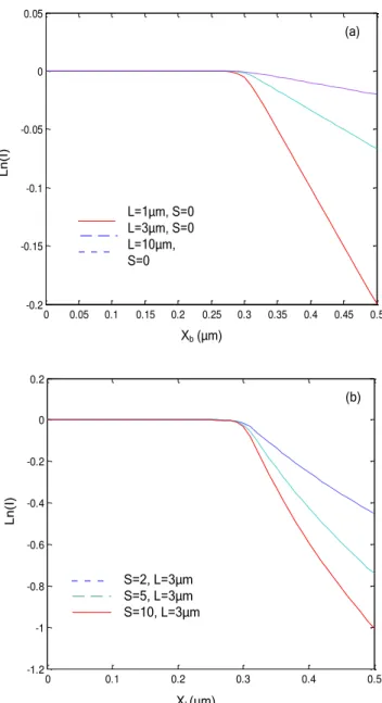
Figure2-15 illustrates EBIC profiles in a normal collector configuration calculated using the approach described above. The sample material is silicon (density of 2.33 g/cm3), and the beam radius is of 10 nm.
0 0.05 0.1 0.15 0.2 0.25 0.3 0.35 0.4 0.45 0.5 -0.2 -0.15 -0.1 -0.05 0 0.05 L=1Njm, S=0 L=3Njm, S=0 L=10Njm, S=0 L n (I ) (a) Xb (Njm) 0 0.1 0.2 0.3 0.4 0.5 -1.2 -1 -0.8 -0.6 -0.4 -0.2 0 0.2 S=2, L=3Njm S=5, L=3Njm S=10, L=3Njm L n (I ) (b) Xb(Njm)
Figure 2-15- EBIC profiles for the region around the edges of a depletion layer located at 0.3μm: (a) different values of the diffusion length L (S=0), (b) different values of the
Chapter references
1- I. M. Watt, "The principles and practice of electron microscopy", Cambridge
University Press, 2nd edition 1997.
2- D. B. Williams, C. B. Carter, "Transmission electron microscopy a textbook for materials science", Springer 2nd edition 2009.
3- S. J. B. Reed, "Electron Microprobe Analysis and Scanning Electron Microscopy in Geology ", Cambridge University Press 2nd edition 2005. 4- L. Reimer, H. Kohl, "Transmission Electron Microscopy, physics of image
formation", Springer 5th edition 2008.
5- R. Oldfield, "Light Microscopy an illustrated guide", Wolfe Publishing 1994. 6- D. A. Newbury, D. C. Joy, P. Echlin, C. E. Friori, and J. I. Goldstein,
"Advanced scanning electron microscopy and X-ray microanalysis", Plenum
Press, New York, 1986.
7- W. Williamson, Jr. and G. C. Duncan, "Monte Carlo simulation of nonrelativistic electron scattering" Am. J. Phys, 54(3), March 1986.
8- N. Tabet, ''Contribution a l'étude des propriétés électriques de volume et des joints de grains dans le germanium application de la méthode du courant induit par faisceau d'électrons EBIC", a thesis submitted for the degree of Doctor of
Philosophy, university of Paris Sud, Centre d'Orsay, 1988.
9- Course note:"Electron Microprobe Analysis by wavelength dispersive X-ray spectrometry", MIT Electron Microprobe Facility.
10- B. G. Yakobi, D. B. Holt, "Cathodoluminescence microscopy of inorganic solids", Plenum Press, New York, 1990.
11- G. Thomas, "Electron microscopy and structure of materials: proceedings",
12- J. Jimenez, "microprobe characterization of optoelectronic material", Taylor &
Francis, 2003.
13- S. Tanuma, K. Nagashima, "Evaluation of an improved absorption correction based on the Gaussian ionization distribution model for quantitative Electron Probe Microanalysis", Mikrochimica Acta [Wien], 299-313, 1983.
14- E. Napchan, "Electron and Photon matter interaction :energy dissipation and injection levels", Revue de Physique Appliqué, colloque C6, supplément au n0 6, tome 24, juin 1989.
15- C. Lamberti, "Characterization of semiconductor heterostructures and nanostructures", Elsevier, Oxford, UK 2008.
16- S. M. Sze, and K. K. Ng, "Physics of semiconductor devices", Wiley, 3rd edition, 2007.
17- D. Donolato, "On the theory of SEM charge-collection imaging of localized defects in semiconductors", Optik, 52(1978/79), No.1, 19-36.
18- F. Berz, and H. K. Kuiken, "Theory of life time measurements with the scanning electron microscope: steady state", Solid State Electronics, vol.19, pp.437-445.
19- A. Jakubowicz, "Transient cathodoluminescence of semiconductors in a scanning electron microscopy", Journal of applied physics. 58(11), pp 4354-4359, Dec 1985.
20- A. Jakubowicz, "Theory of cathodoluminescence contrast from localized defects in semiconductors", Journal of applied physics. 59(6), pp 2205-2209, March 1985.
21- T. S. Rao-Sahib and D. B. Wittry, "Measurment of diffusion lengths in p-type Galium Arsenide by electron beam excitation", Journal of applied physics. 40(9), pp 3745-3750, 1969.
22- W. Hergert, S. Hildebrandt, L. Pasemann, "Theoretical investigations of combined EBIC, LBIC, CL and PL experiments", Phys. Status. Solidi, (a) 102, 819(1987).
23- W. Hergert, and L. Pasemann, "Theoretical study of the information depth of the cathodoluminescence signal in semiconductor materials", Phys. Status.
Solidi, (a) 85, 641(1984).
24- W. Hergert, P. Reck, L. Pasemann, and J. Schreiber, "Cathodoluminescence measurements using the scanning electron microscope for the determination of semiconductor parameters", Phys. Status. Solidi, (a) 101, 611(1987).
25- J. C. H. Phang, K. L. Pey, D. S. H. Chan, "A simulation model for cathodoluminescence in the Scanning Electron Microscopy". IEEE
transactions on electron devices, vol 39(4), Apr 1992.
26- C. J. Wu, D. B. wittry, "investigation of minority-carrier diffusion lengths by electron bombardment of Schottky barriers". J. App. Phys, Vol. 49. (5). May. 1978.
27- C. Donolato, "On the analysis of diffusion length measurements by SEM",
Solid State Electronics, Vol. 25, No. 11, pp. 1077-1081, 1982.
28- Kurniawan. O, Ong. V. K. S, "Choice of generation volume models for electron beam induced current computation", IEEE Transactions on Electron
29- O. Kurniawan , "device parameters characterization with the use of EBIC", Phd thesis (supervisor Pr O. V. Ong), Nanyang Technological University, 2008.
30- Nouar. Tabet, "Contribution a l'étude des propriétés électriques de volume et des joints de grains dans le germanium application de la méthode du courant induit par faisceau d'électrons EBIC", Phd thesis, University of Paris Sud centre d'Orsay.