HAL Id: hal-01582538
https://hal.archives-ouvertes.fr/hal-01582538
Submitted on 6 Sep 2017
HAL is a multi-disciplinary open access
archive for the deposit and dissemination of
sci-entific research documents, whether they are
pub-lished or not. The documents may come from
teaching and research institutions in France or
abroad, or from public or private research centers.
L’archive ouverte pluridisciplinaire HAL, est
destinée au dépôt et à la diffusion de documents
scientifiques de niveau recherche, publiés ou non,
émanant des établissements d’enseignement et de
recherche français ou étrangers, des laboratoires
publics ou privés.
Copyright
Nicolas Chevalier, Olivier de Sagazan, Alain Le Corre, Hervé Folliot, Mehdi
Alouini
To cite this version:
Fethallah Taleb, Salvatore Pes, Cyril Paranthoen, Christophe Levallois, Nicolas Chevalier, et al..
Enhancement of VCSEL Performances Using Localized Copper Bonding Through Silicon Vias. IEEE
Photonics Technology Letters, Institute of Electrical and Electronics Engineers, 2017, 29 (13), pp.1105
- 1108. �10.1109/LPT.2017.2703599�. �hal-01582538�
Abstract— We report on a new cost effective, with a low
temperature budget and simple bonding process on silicon, presenting efficient heat spreading and great potentialities in integration. This process is based on a thick electro-plated copper bonding layer through silicon vias and is expected to reduce significantly the bonded device internal temperature. We apply this process to realize 1.55 µm emitting vertical-cavity surface-emitting lasers. We demonstrate continuous wave operation from room temperature up to 55°C, an internal temperature reduction of 13°C, and we estimate a decrease of 30% of the overall device thermal impedance.
Index Terms—bonding processes, thermal management, wafer
scale integration, Vertical-cavity-surface-emitting-laser
I. INTRODUCTION
ONDING technologies have encountered over the years growing interests and developments, covering a wide panel of applications. Starting from the 3D integration in microelectronics, bonding processes are commonly used in the fabrication of micro electro-mechanical systems [1], in heat flow management for high power transistors or photonic devices [2], [3], and more recently in the emerging development of silicon photonics and heterogeneous integration of III-V compounds on a mature silicon platform [4] [5] [6]. In most cases, the bonding of two (or more) different (or not) substrates allows improving the device performances, or the emergence of new components and functionalities which would otherwise not be possible.
Among the different bonding approaches, Van Der Waals (VDW) and polymer adhesive bonding are commonly used
This work was supported by Agence Nationale de la Recherche and Direction Générale de l'Armement within the ANR-ASTRID HYPOCAMP project (grant ANR-14-ASTR-0007-01) and a DGA-MRIS/Région Bretagne fellowship (grant ARED-VELOCE 8917).
F. Taleb, S. Pes, C. Paranthoen, C. Levallois, N. Chevalier, A. Le Corre, O. Durand, H. Folliot, M. Alouini are with UMR FOTON, CNRS, INSA de Rennes, Université de Rennes 1, F-35708 Rennes, France (email : [email protected], [email protected], [email protected], [email protected], [email protected], [email protected], [email protected], [email protected])
O. De Sagazan is with UMR IETR, CNRS, Université de Rennes 1, F-35042 Rennes, France (email : [email protected])
attractive. Both technologies enable to bond individual chips or whole wafers onto silicon substrates , with the constraint to process extremely flat surface in the case of the VDW method (commonly SiO2 layers are used in conjunction with chemical
mechanical polishing technologies (CMP)) [7], whereas the polymer adhesive bonding technique is less restrictive on the surface roughness when adhesive layers such as benzocyclobutene (BCB) are used. [6]. Considering these two bonding methods, III-V materials based devices such as lasers and photodiodes have been successfully bonded onto silicon photonic platforms [4] [5] [6]. In both cases the thermal management is still an important challenge, which may limit the overall device performances, mainly because of the poor thermal conductivity of the insulated layers used for the bonding. When the thermal budget of the bonded devices is too large, as in the case of InP-based vertical-(external)-cavity surface-emitting lasers (V(E)CSELs), metallic bonding on a diamond substrate or the use of a metallic heat-spreader have been reported to drastically improve the device performances [8], [9]. Nevertheless, in this case, the integration with silicon microelectronic or photonic platforms is mechanically not possible. As an alternative, the flip-chip process, consisting in bonding devices to silicon via metallic bumps, has been developed with success, leading to significant improvements in VCSEL performances, along with the benefits of the silicon platform integration [10]. Recently, we have proposed a new hybrid bonding process, called the TSHEC process (standing for Trough Silicon Holes Electroplated Copper bonding), which combines the advantages of the integration on a silicon platform, with the thermal improvement inherent to the use of a copper metallic bond layer acting as a localized efficient heat-spreader and contact layer [11]. In this letter we apply this process to the fabrication of InP-based VCSELs operating at telecommunication wavelength. We report improvements of VCSEL performances, and we present experimental evidences showing significant reduction of the device thermal impedance below 1000 K/W, as expected according to finite element method (FEM) simulations. These results evidence the potentialities of the TSHEC process, allowing the hybrid integration of virtually any photonic or microelectronic device on a silicon platform, while keeping a thermally efficient, cost-effective and simple process.
Enhancement of VCSEL performances using
localized copper bonding through Silicon vias
F. Taleb, S. Pes, C. Paranthoen, C. Levallois, N. Chevalier, O. De Sagazan, A. Le Corre, H. Folliot
and M. Alouini.
realized according to the TSHEC process is depicted in Fig. 1. It mainly consists of two distinct parts. The first one is the host silicon substrate, on which matrices of 3x3 square holes have been realized by anisotropic wet etching, with typical dimensions of 200x200 µm2 and 700x700 µm2 on both sides of the substrates. The second part is the VCSEL structure, designed to operate under optical pumping. It consists in 9 strained InGaAsP quantum wells, distributed over three optical standing wave anti-node positions, and emitting at 1.52 µm, grown by gas source molecular beam epitaxy on InP(001) substrate. A red shift of 30 nm has been considered for the design of the cavity mode resonance, in order to obtain a VCSEL emission at 1.55 µm during room temperature operation of the device. A first hybrid distributed Bragg reflector (H-DBR), consisting in 3.5 periods of amorphous silicon (aSi) and amorphous silicon nitride (aSiN) dielectric layers, completed by a final 200 nm-thick gold layer, is deposited, with a theoretical reflectivity of 99.66%. Dry etching is performed on the H-DBR to form circular mesas with diameters varying from 20 µm up to 100 µm. A metallic layer of Ti/Au is then deposited on the whole substrate, acting as the electrode for a next electroplating step.
Fig. 1. Cross section view of the TSHEC VCSEL.
At this stage, a 3 µm-thick BCB layer is spin-coated on the processed InP substrate. The silicon host and InP substrates are aligned one to each other to center the H-DBRs within the 200x200 µm2 wide silicon holes. Both substrates are then brought into contact and the BCB is cured to finalize the pre-bonding step. A dry etching step is performed through the silicon backside (presenting the 700x700 µm2 wide holes) to remove the unprotected BCB from the metallic layer, leaving the H-DBRs uncovered, as shown on the Fig. 2 (a). Then, electroplating is performed on the metallic layer through the holes, leading to a partial filling of the silicon vias with a 50 µm thick Cu layer, and completely covering the H-DBRs (which in the following will be called BDBR for buried H-DBR), as shown on Fig. 2(b). This copper layer enables a robust mechanical link with the silicon substrate while also promoting the heat spreading from the device, thereby acting as a localized and efficient heat sink. Note that this copper layer can be also used as contact layer if an electrical pumping scheme is implemented for such devices. Following this step, the whole InP substrate is removed by a combination of mechanical and chemical etching, down to an InGaAs stop
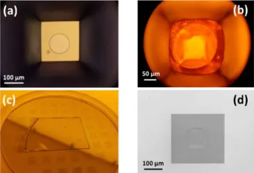
Fig. 2(c) presents a picture of a quarter of 2 inches VCSEL wafer bonded onto the silicon substrate just after the substrate removal. It shows a uniform mirror like surface, presenting none defects like air gap or unbounded related “bubbles” or any scribe lines. Also, we can notice apart from the VCSEL sample several 3×3 black square patterns corresponding to the silicon holes matrices which remain not used in this case. It is worthwhile to notice also that the TSHEC technique has no limitation in terms of size for the processed wafers, allowing bonding a complete 2-inches (or more) wafer on a corresponding Si host substrate.
Fig. 2 : Images representing the 100 µm diameter H-DBR VCSEL fabrication according to the TSHEC process at different step : (a) after the BCB dry etching and (b) after the Cu electroplating (both views through a silicon hole), (c) whole wafer after the InP substrate removal, (d) SEM image of a 400×400 µm² InP VCSEL die on silicon at the end of the process.
This half VCSEL structure is completed by the deposition of the top DBR, consisting in four pairs of aSi/aSiN with a theoretical reflectivity of 99.3 %. The process is completed by the definition of VCSEL individual dies (400×400 µm²), as shown on Fig. 2(d), according to conventional photolithography steps and dry etching of the DBR and InP layers.
III. TSHECVCSEL CHARACTERIZATIONS
VCSEL devices have been characterized under optical excitation, with a 980 nm continuous wave (CW) laser diode, focused on a 15-20 µm in diameter spot (1/e² waist size). Temperature is controlled with a Peltier module controller. Measurements are performed on VCSEL devices presenting different BH-DBR diameters, from 20 up to 100 µm, and belonging from the same 3×3 matrix (see Fig. 2(c)). This very restricted surface (6.7 mm²) enables to exclude any MBE related microcavity and/or DBR thicknesses inhomogeneity.
Fig. 3 (a) and (b) represent the VCSEL light output power as a function of the absorbed pump power (LL characteristic) measured at different device temperature and for two VCSELs integrating a BH-DBR diameter of 100 µm and 20 µm respectively. Note that for all measurements, a peculiar
attention has been paid to the VCSEL optical excitation, in order to maintain a single transverse mode emission, as evidenced by the Fig. 3 (a) and (b) inset representing typical single transverse mode near field intensity and spectrum measured from VCSELs. This peculiar point is important for reliable LL curves, but also for the estimation of the thermal impedance measurements, which will be presented later in the paper. As shown on Fig .3 (a), the 100 µm BH-DBR VCSELs exhibits laser operation from room temperature up to 50°C, with a typical threshold power of 9 mW and a maximal output power of 2.5 mW, measured respectively at 16°C. The external quantum efficiency is decreasing from 0.6 down to 0.45 with temperature increasing from 16°C up to 50°C. Fig 3(b) represents the same LL characteristics in the case of the 20 µm BH-DBR VCSEL. At 16°C, a smaller threshold of 6 mW is obtained with a 2 mW maximal output power. From 16°C up to 50°C, a low efficiency of 0.08 is measured, being constant in the whole temperature range.
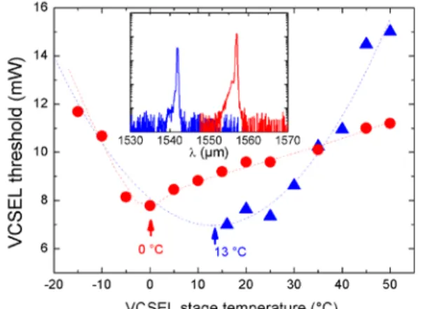
We attribute this lower value to the experimental set-up itself, considering that this 20 µm diameter BH-DBR and the incident pump spot are very close in size to each other. This might induce an overestimation of the real absorbed power, which may mainly explain the lower slope efficiency for the 20 µm diameter BH-DBR VCSEL, rather than any other additional detrimental effect. Nevertheless, from this experiment, we can retain that in comparison with the 100 µm BH-DBR, the 20 µm BH-DBR VCSEL threshold is lower. Fig. 4 represents both VCSELs threshold power as a function of the VCSEL stage temperature, from 50°C down to -15°C. For temperatures lower than the dew point (Tdew≈15°C),
measurements have been performed under an oversaturated nitrogen atmosphere. Note that in the case of the 20 µm BH-DBR VCSEL, measurements in the low temperature range have not been performed, because such small devices have been partly destroyed with an unintended exposure to moisture. As a usual procedure on VCSEL [6] [9], we proceed to a simple second order polynomial fit to estimate that the minimum threshold is achieved at a temperature of 13°C for such a device. For the 100 µm BH-DBR VCSEL, the
minimum threshold is measured at a temperature of 0°C. Also, Fig. 4 inset represents the optical emission spectra of both VCSELs, measured respectively at 13 °C and 0 °C. The 20 µm BH-DBR VCSEL (blue spectra) presents a 15 nm blueshift in comparison with the 100 µm one. Both measurements clearly indicate that the VCSEL internal temperature is lower in the case of the 20 µm BH-DBR, enabling to get a smaller wavelength emission when the matching between the modal gain and the cavity resonance is achieved. These results can be ascribed to an experimental evidence of a better heat spreading from the device when a smaller BH-DBR is combined with the TSHEC process.
Fig. 4 : VCSEL threshold power as a function of the VCSEL stage temperature for the 100 and 20 µm BH-DBR VCSELs (red dots and blue triangles respectively). Red dotted curve is only for eye-guiding, the blue dotted curve is a second order polynomial fit. In inset, the VCSEL emission spectra measured at 0°C and 16°C for the 100 µm and 20 µm BH-DBR VCSEL (red and blue), respectively.
Going further, the thermal properties of VCSEL devices have been investigated thanks to Finite Element Modelling (FEM) calculations. According to the VCSEL design depicted on Fig. 1, the thermal impedance (Rth) is extracted from FEM
simulations for different BH-DBR diameters, by measuring the internal VCSEL temperature gradient when a 15 µm-diameter heat spot of 15 mW is absorbed within the active layer. In Fig. 5 is represented the result of such simulations. The case in which a 3 µm-thick large-area BCB layer is used for the device bonding on Si (blue circles) is compared to case in which the TSHEC process is used (dark squares). In the first case, a large thermal impedance of 2800 W/K is deduced for a 100 µm BH-DBR, which is getting even worse when the BH-DBR diameter is reduced. This is mainly due to the bad thermal conductivity of the BCB layer, in comparison with the one offered by the combination of the BH-DBR and the localized copper heat-spreader. Indeed, in the case of the TSHEC design, for devices presenting a BH-DBR larger than 50 µm, a reduced and constant thermal impedance of 1250 W/K is deduced. This is mainly limited by the BH-DBR thermal impedance itself, the reflector being composed by dielectric materials. Reducing the BH-DBR diameter below 50 µm favors the heat flow spreading from the VCSEL device towards the copper layer across the InP layers surrounding the pumped area. As a consequence, from this simulation we deduced a decrease of 11°C for the 20 µm BH-DBR device maximal internal temperature in comparison with the 100 µm
Fig. 3 : CW VCSEL output power as function of the absorbed pump power measured at different temperatures (from 16°C up to 50°C) for (a) the 100 µm and (b) the 20 µm BH-DBR VCSEL. Insets correspond to typical near field intensity profile and spectrum measured at 16°C from VCSELs with an output power emission of 1.5 mW.
close to the 13°C previously presented on Fig. 4. As a first glance, the overall tendency obtained with the FEM modeling is fully in agreement with the previously presented experimental data and the assumptions considering superior thermal performances of the TSHEC process when smaller BH-DBR is used.
To appreciate the benefits of the TSHEC process, we compare the FEM simulations with the experimental results we obtain from our devices. The red stars on the Fig. 5 are the experimental values of the VCSEL Rth we deduce from the
linear redshift of the VCSEL emitting wavelength with respect to the temperature (∆𝜆 Δ⁄ 𝑇), and the absorbed power (∆𝜆 Δ𝑃⁄ 𝑎𝑏𝑠),measured at 16°C(not shown) [9]. For large BH-DBR diameters of 80 and 100 µm, we measured a Rth of
1000-1050 K/W, which is close to the one calculated by FEM simulations. For a BH-DBR diameter of 50 µm, a clear decrease of the Rth is measured down to 740 W/K, evidencing
better heat spreading. It is followed by an increase for the 20 µm BH-DBR. Once again, as previously discussed for such small BH-DBR diameter, we considered this unexpected increase of Rth for the 20 µm diameter BH-DBR to be mainly
the consequence of the optical pumping set up. This value has to be considered with precaution, if we take into account the above experimental evidences showing the superior thermal properties of this 20 µm BH-DBR VCSEL.
IV. CONCLUSION
We demonstrate 1.55 µm VCSEL CW operation with improved thermal performances, by applying a new process to bond the device on a silicon platform. This process consists in bonding a semiconductor active region (but virtually any semiconductor material) on a Si host platform, through the use of electroplated Cu through Si vias acting as localized micro-heat sinks, enabling a robust bonding of the devices as well as benefiting from improvements in the thermal impedance of the
reduction of 13°C. We estimate that this process enables to decrease the thermal resistance for this VCSEL device by 30%. Following this proof-of-concept demonstration of this TSHEC bonding process, and since it is fully compatible with optical or electrical pumping schemes, other devices suffering from a high thermal budget can successfully been tested, such as high power lasers and LEDs, or high power transistors. Finally, as this process bonding uses a silicon host substrate, it can be envisaged to implement some chip functions on the silicon platform, such as a temperature monitoring or a device driver, to further improve the device integration.
REFERENCES
[1] M. Lapisa, G. Stemme, and F. Niklaus, “Wafer-Level Heterogeneous Integration for MOEMS, MEMS, and NEMS,” IEEE J. Sel. Top. Quantum Electron., vol. 17, no. 3, pp. 629–644, May 2011.
[2] K. K. Chu et al., “High-Performance GaN-on-Diamond HEMTs Fabricated by Low-Temperature Device Transfer Process,” 2015, pp. 1–4.
[3] S. T. Keller, A. Sirbu, V. Iakovlev, A. Caliman, A. Mereuta, and E. Kapon, “85 W VECSEL output at 1270 nm with conversion efficiency of 59 %,” Opt. Express, vol. 23, no. 13, p. 17437, Jun. 2015.
[4] M. Lamponi et al., “Low-Threshold Heterogeneously Integrated InP/SOI Lasers With a Double Adiabatic Taper Coupler,” IEEE Photonics Technol. Lett., vol. 24, no. 1, pp. 76–78, Jan. 2012.
[5] N. Hattasan, A. Gassenq, L. Cerutti, J.-B. Rodriguez, E. Tournie, and G. Roelkens, “Heterogeneous Integration of GaInAsSb p-i-n Photodiodes on a
Silicon-on-Insulator Waveguide Circuit,” IEEE Photonics Technol.
Lett., vol. 23, no. 23, pp. 1760–1762, Dec. 2011.
[6] E. P. Haglund et al., “Silicon-integrated
short-wavelength hybrid-cavity VCSEL,” Opt. Express, vol. 23, no. 26, p. 33634, Dec. 2015.
[7] J. M. Fedeli et al., “Development of Silicon Photonics Devices Using Microelectronic Tools for the Integration on Top of a CMOS Wafer,” Adv. Opt. Technol., vol. 2008, pp. 1–15, 2008.
[8] Z. Zhao et al., “Cost-Effective Thermally-Managed 1.55 µm VECSEL With Hybrid Mirror on Copper
Substrate,” IEEE J. Quantum Electron., vol. 48, no. 5, pp. 643–650, May 2012.
[9] T. Grundl et al., “Record Single-Mode, High-Power VCSELs by Inhibition of Spatial Hole Burning,” IEEE
J. Sel. Top. Quantum Electron., vol. 19, no. 4, pp.
1700913–1700913, Jul. 2013.
[10] K. S. Kaur, J. Missinne, and G. Van Steenberge, “Flip-chip bonding of vertical-cavity surface-emitting lasers using laser-induced forward transfer,” Appl. Phys. Lett., vol. 104, no. 6, p. 061102, Feb. 2014.
[11] F. Taleb et al., “Substrate bonding using electroplated copper through silicon vias for VCSEL fabrication”,
Proc IEEE Indium Phosphide Related Material (IPRM)
2014.
Fig.5 : Thermal impedance of the VCSEL calculated for different BH-DBR diameters, when a 3 µm-thick BCB layer is used for the bonding (blue circles), and in the case of the TSHEC process (dark squares). Red stars are experimental values deduced from experiments on several tested VCSEL samples.