This is an author-deposited version published in: http://oatao.univ-toulouse.fr/ Eprints ID: 8951
To cite this version:
Cisse, Alioune and Vidal, Paul-Etienne and Massiot, Gregor and Munier, Catherine and Carrillo, Francisco Numerical modelling of a high temperature power module technology with SiC devices for high density power electronics. (2012) In: PCIM Europe, Power Electronics - Intelligent Motion - Renewable Energy - Energy Management, 8-10 may 2012, Nuremberg, Germany.
O
pen
A
rchive
T
oulouse
A
rchive
O
uverte (
OATAO
)
OATAO is an open access repository that collects the work of Toulouse researchers and makes it freely available over the web where possible.
Any correspondence concerning this service should be sent to the repository administrator: [email protected]
Numerical modelling of a high temperature power module
technology with SiC devices for high density power
elec-tronics
Alioune Cissé1, 2, *, Gregor Massiot1, Catherine Munier1, Paul-Etienne Vidal2, Francisco Carrillo2
1EADS France – Innovation Works, 12 rue Pasteur 92152 Suresnes, France
2University of Toulouse - INP Toulouse – LGP, 47 avenue d’Azereix 65016 Tarbes, France *Tel.: +33 (0) 5 62 96 61 62
*E-Mail: [email protected]
Abstract
This paper presents the development of a new packaging technology using silicon carbide (SiC) power devices. These devices will be used in the next power electronic converters. They will provide higher densities, switching frequencies and operating temperature than current Si technologies. Thus the new designed packaging has to take into account such new constraints. The presented work tries to demonstrate the importance of packaging de-signs for the performance and reliability of integrated SiC power modules. In order to in-crease the integrated density in power modules, packaging technologies consisting of two stacked substrates with power devices and copper bumps soldered between them were pro-posed into two configurations. Silver sintering technique is used as die-attach material solu-tion. In order to assess the assembling process and robustness of these packaging designs, the thermo-mechanical behaviour is studied using FEM modelling. Finally, some recommen-dations are made in order to choose the suitable design for reliable power modules.
1.
Introduction
The emergence of wide band gap semiconductors such as SiC enables power converters to operate at high switching frequency with better power conversion efficiencies and at temper-atures beyond 200°C. The switching frequency defines primarily the size of passive compo-nents, such as inductors and transformers, used in converters for transient storage and filter-ing. A significant weight reduction can be expected. Moreover, the cooling requirements are much less stringent, and wide band gap semiconductors allow us to reduce the cooling sys-tem, leading to improvements in power density. This also contributes to the expected weight reduction.
To achieve the high density integration requirements for SiC power devices, classical alu-minium wire bonding is replaced by copper bump interconnection in the superposition of two substrates in a sandwich. Firstly, bump interconnections have a larger diameter than the wire bonds and hence less parasitic inductance. They also offer the potential of lower resistance. The current capability is also increased. Secondly, they offer two thermal paths to dissipate the heat to the substrates. They play the role of thermal drain and stand-off elements be-tween substrates for electrical isolation after gel filling [1]. This packaging solution improves the electrical and thermal characteristics, reduces the packaging size and present more power integration possibilities [2]. In order to realize reliable sandwich packaging, several high temperature solder alloys using low temperature processes are identified. Among these processes, there is the nano or micro-paste silver sintering technique. These processes could minimize the thermo-mechanical stresses and increase the reliability in high tempera-ture operation [3]. In this work, the sintered silver is studied as solder joint to ensure the die-attach and also the bump interconnections. The process combines a low pressure to de-crease the porosity ratio in the joint and a fixed temperature profile between 275°C and 325°C during 10 min. The temperature is chosen according to the metal powder.
The objectives of this paper are to assess the reliability of sandwich packaging technologies. Thus their thermo-mechanical behaviours were calculated and compared under thermal cy-cling between -40°C and +185°C. These results take into account the residual stresses in-duced by the sintering process at 275°C.
2.
Assembly technologies
2.1.
Sandwich packaging
The sandwich packaging consists in stacked substrates with semiconductor devices be-tween them. The solder bump technique is used to realize the device top-side interconnec-tions such as flip-chip BGA interconnects [4]. If the process is made by soldering, it usually requires three successive reflow phases and hence three different solder alloys with different melting temperatures. For the new high temperature power module, the successive reflow phases constitute an issue. For example, the range of available temperatures for the as-sembly process is much smaller, because the semiconductor devices have a maximum pro-cess temperature. This is of course directly linked with solder alloys allowed. To bypass the difficulty, the proposed packaging technology consists in using low temperature sintering in-stead of soldering, with silver paste. This assembly process is applied to minimize the ther-mal stresses induced by a multi-reflow process. However, particular designs are required to ensure large contact areas so as to achieve reliable assemblies, and to reduce the thermo-mechanical stresses concentration in the bump interconnections during the assembling pro-cess.
2.2.
Silver sintering process
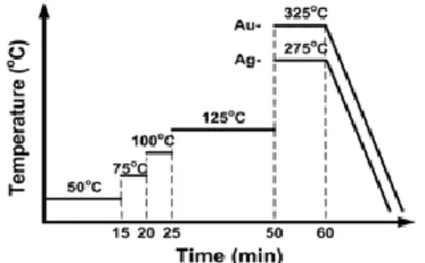
Low temperature sintering technique is an approach for high temperature lead-free solders. This technique uses silver paste as die-attach and bump solder. It can be achieved by three ways. The first way consists in using a silver micro-paste which is heated at 250°C with an applied hydrostatic pressure from 20 MPa to 40 MPa to increase the joint density [5]. The second way consists in using silver particles of a nano-scale. In such solution [6], the addi-tional organic components such as solvent were selected so as to eliminate the applied pressure. In this case, silver nano-paste can be heated at 275°C to 325°C under standard atmospheric pressure and thus the density of sintered silver can reach 80% of bulk silver. Figure 1 shows the nano-silver sintering profile on gold (Au) and silver (Ag) metallization which is used in this study.
Fig. 1. Nano-paste silver sintering profile on Au and Ag final metal on devices [7]
The advantage of this technique is that once the silver nano-paste is sintered, it will have a high melting point such as bulk silver (961°C). Therefore this technique allows successive sintering operations. Consequently, the issue of using several eutectic solder alloys is re-moved. Another sintering technique has been newly developed by Heraeus and uses a silver micro-paste especially created for small die area less than 50 mm2. In such case no pres-sure is required and the sintering process is simplified. It could be in a single step.
3.
Numerical design and modelling
3.1.
Packaging designs
Assembly configurations
The assembly configuration selection is defined based on the assembly technology review literature. They allow higher integration levels and double-side cooling to improve the ther-mal management. The copper bump may vary in shape and size as illustrated in figure 2.
AMB SUBSTRATE AMB SUBSTRATE SiC DEVICE COPPER BUMP SINTERED SILVER AMB SUBSTRATE AMB SUBSTRATE SiC DEVICE COPPER BUMP SINTERED SILVER AMB SUBSTRATE AMB SUBSTRATE SiC DEVICE COPPER BUMP SINTERED SILVER AMB SUBSTRATE AMB SUBSTRATE SiC DEVICE COPPER BUMP SINTERED SILVER (a) (b)
Fig. 2. Elementary packaging designs for finite element models : Spherical copper bump (a) and
cy-lindrical copper bump (b)
The geometries of elementary packaging structures are based on standard thicknesses used also in automotive and railway power modules. The power SiC devices are 440.4 mm3, ceramic substrates are 660.64 mm3, the metallization is 200 µm height, the consid-ered solder joints thickness is100 µm, truncated spherical bump is diameter 2 mm height 1.5 mm and cylindrical bump is diameter 1 mm length 1 mm.
Materials, thermal and mechanical parameters
The materials used in these packaging studies are SiC for power devices, silicon nitride (Si3N4) for ceramic substrates with copper (Cu) as metallization and silver as sintered joint. The thermal and mechanical properties of these materials were extracted from literature re-garding their thermal conductivity, coefficient of thermal expansion, Young’s modulus, Pois-son’s ratio …etc [8, 9], as presented in table below.
Properties Cu SiC Si3N4 Sintered Ag [9]
(W.K-1.m-1) 398 130 60 416
(kg.m-3) 8850 3210 3290 104
(10-6.K-1) 17.3 4.8 3.3 19.6
C (J.kg-1.°C-1) 380 800 800 230
E (GPa) 128 460 310 See table below
0.36 0.18 0.27 0.37
Yield Stress (MPa) 98.7 610 - -
Temperature (°C) -40 0 25 60 120 150 E (GPa) 9.01 7.96 6.28 4.52 2.64 1.58
3.2.
Finite element modelling
Materials constitutive law and parameters
The model of the sintered silver joint is simulated with Anand’s unified visco-plastic constitu-tive model [9]. Equations (1), (2) and (3) give the formulation of Anand’s model [10]. It mod-els the inelastic deformation behaviour of the silver joint used as die-attach and solder bump interconnection.
m
s
RT
Q
1sinh
exp
(1), n RT Qe
s
s
ˆ
* (2),
01
*.
1
*s
s
sign
s
s
h
h
a (3) Where
is the inelastic strain rate, is the inelastic strain, Q is the activation energy, A is the pre-exponential factor, is the multiplier of stress, m is the strain rate sensitivity, R is the gas constant, s is the coefficient of deformation resistance, is the equivalent stress and T is the absolute temperature. The quantitys
*represents a saturation value of s. sˆ is a coefficient for the saturation value of deformation resistance. h is a strain hardening function.To complete the nine parameters of Anand’s visco-plastic model (see table below) [9], there are: the initial value of deformation resistance s0, the hardening constant h0, the strain rate
sensitivity of saturation value n and the strain rate sensitivity of hardening a. These parame-ters were identified between -40°C and 185°C.
s0 (MPa) Q (J.mol-1) A (s-1) m h0 (MPa) sˆ (MPa) n a
2.768 47442 9.81 11 0.6572 15800 67.389 0.00326 1
They have been assigned through the input for VISCO107 element in ANSYSTM software for the simulation.
Thermal cycling load
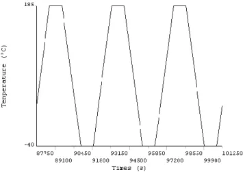
The packaging process and endurance are assessed using finite element method for two bump configurations as shown in figure 3. In order to evaluate the robustness of these pack-aging designs, their thermo-mechanical behaviour is studied under 3 thermal cycling loads as shown in figure 3, taking into account the validity temperature range of previous Anand’s parameters. The profile begins at 25°C initial temperature, the ramp rate is 10°C/min and the dwell times are 15 min at -40°C and 185°C.
Fig. 3. Thermal cycling profiles: -40°C, +185°C
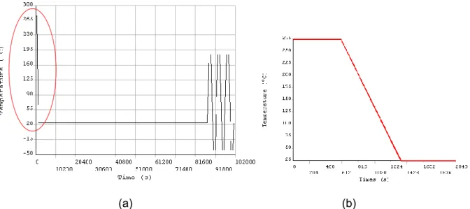
Assembling process coupled with thermal cycling load
The simulation takes into account the residual stresses induced by the assembling process. In this paper only the last step of the silver sintering process is also simulated as shown in figure 4(b). That means a dwell time of 10 min at 275°C and a ramp rate of 20°C/min before starting the 3 thermal cycles described in figure 3. Thus a stress relaxation is applied after the sintering process during 24 hours at 25°C. After what, the thermal cycling load between -40°C and 185°C is conducted (figure 4(a)).
(a) (b)
Fig. 4. Thermo-mechanical stress profile applied for simulation (a), zoom on assembling profile (b)
3.3.
Simulation results
The stress distribution and the total mechanical strain are plotted after the assembling pro-cess and also at the end of the thermal cycling load. Thus the thermo-mechanical behaviour of each bump configuration is compared after assembling process and thermal cycles.
5(a)
5(b)
Fig. 5. Stress distribution [Pa] 5(a) and mechanical strain 5(b) in cylindrical bump after assembling
process
= 34 MPa
6(a)
6(b)
Fig. 6. Stress distribution [Pa] 6(a) and mechanical strain 6(b) in cylindrical bump at the end of 3
thermal cycles
7(a)
7(b)
Fig. 7. Stress distribution [Pa] 7(a) and mechanical strain 7(b) in spherical bump after assembling
process
= 34 MPa
= 0.7%
= 3 MPa
8(a)
8(b)
Fig. 8. Stress distribution [Pa] 8(a) and mechanical strain 8(b) in spherical bump at the end of 3
ther-mal cycles
3.4.
Influence of Solder bump geometry on packaging behaviour
The simulation results show that the maximal strains are located in the silver sintered joints. Thus, the bump joint interface seems to be the more critical zone in the packaging. However, it can be noted that the spherical bump joint presents less strain level than a cylindrical one (=0.12% against =0.7%) after the assembling process, as shown on figures 5(b) and 7(b). At the end of thermal cycling loads, these values remain stable at respectively 0.12% and 0.7% (figures 6(b) and 8(b)).
Concerning the stress distribution, the cylindrical bump joint presents a maximal stress of about 34 MPa after the sintering process and also 34 MPa at the end of thermal loads ures 5(a) and 6(a)). While the spherical bump joint presents a maximal stress of 3 MPa (fig-ures 7(a) and 8(a)). These results show that the maximal stress distribution in the spherical configuration were more than 10 time lower than the cylindrical one. The results also confirm the evolution of the total mechanical strain during the thermal cycling loads. For each bump design, the stress-strain evolution is similar during the thermal-mechanical constraints. The bump designs with large contact areas appear to be suitable for sandwich packaging using silver sintered as solder joint solution (figure 2(a)).
4.
Conclusion
The objective of this study was to evaluate new packaging technologies for high temperature and high power density SiC devices. In this study, these technologies were simulated with new developed materials and assembling process. The influence of die-attach and solder bump configurations were studied in order to meet the power applications requirements. In order to increase the power density, a technology consisting of two stacked substrates with power devices soldered between them, was proposed with good perspectives. The
de- = 3 MPa
velopment of the new silver sintering techniques allows us to remove the use of several sol-der alloys.
Hence, to assess reliable sandwich packaging, FEM modelling and simulation were con-ducted on two packaging configurations to evaluate and compare the thermo-mechanical behaviours. These calculations take into account the residual stresses induced by the as-sembling process.
It could be noted that the solder bump design plays a fundamental role in the packaging as-sembly and reliability. Then, the results point-out the use of truncated spherical solder bump as the better solution.
5.
Literature
[1] Calata, J. N., Bai, J. G., Liu, X., and, al.,, “Three dimensional packaging for power semiconductor devices and modules,” IEEE Transactions on Advanced Packaging, Vol. 28, no. 3, pp. 404-412,
August 2005.
[2] M. Mermet-Guyennet, “New structure of power integrated module,” CIPS 2006, Naples, June
2006.
[3] Bai, G., “Low-Temperature Sintering of Nanoscale Silver Paste for Semiconductor Device Inter-connection,” PhD thesis, Virginia Polytechnic Institute and State University, Blacksburg, Virginia,
October 2005.
[4] X. Liu, S. Haque, and G.-Q. Lu, “Three-dimensional flip chip on flex packaging for power electron-ics application,” IEEE Trans. Adv. Packaging, vol. 24, no. 1, pp. 1–9, Feb. 2001.
[5] Z. Zhang and G. Q. Lu, “Pressure-assisted low-temperature sintering of silver paste as an alterna-tive die-attach solution to solder reflow,” IEEE Trans. Electron. Packaging. Manufacture, vol. 25,
no. 4, pp. 279–283, Oct. 2002.
[6] Zhang, Z., J. N. Calata, J. G. Bai, and G-Q. Lu. “Nanoscale Silver Sintering for High-Temperature Packaging of Semiconductor Devices.” in Proc. of 2004 TMS Annual Meeting & Exhibition. 2004.
Charlotte, NC.
[7] Guo-Quan Lu, J. N. Calata, G. Lei, and X. Chen, “Low-temperature and Pressure less Sintering Technology for High-performance and High-temperature Interconnection of Semiconductor Devic-es,” 8th. Int. Conf. on Thermal, Mechanical and Multi-physics Simulation and Experiments in
Mi-cro-Electronics and Micro-Systems, EuroSime 2007
[8] MatWeb, “The Online Materials Database” www.matweb.com .
[9] Yu D. J., Gang C., Wang Z., and G-Q. Lu, “Applying Anand model to Low-Temperature sintered nanoscale Silver paste chip attachment,” Trans. On Materials and Design, 30: p. 4574 – 4579,
2009.
[10] J. Wilde, K. Becker, M. Thoben, W. Blum, T. Jupitz, G. Z. Wang, Z. N. Cheng, “Rate dependent constitutive relations based on Anand model for 92.5Pb5Sn2.5Ag solder,” IEEE Transactions on

![Fig. 6. Stress distribution [Pa] 6(a) and mechanical strain 6(b) in cylindrical bump at the end of 3 thermal cycles](https://thumb-eu.123doks.com/thumbv2/123doknet/3629694.106724/7.892.156.729.108.576/fig-stress-distribution-mechanical-strain-cylindrical-thermal-cycles.webp)
![Fig. 8. Stress distribution [Pa] 8(a) and mechanical strain 8(b) in spherical bump at the end of 3 ther- ther-mal cycles](https://thumb-eu.123doks.com/thumbv2/123doknet/3629694.106724/8.892.168.724.105.578/fig-stress-distribution-mechanical-strain-spherical-bump-cycles.webp)
