i
UNIVERSITÉ DE SHERBROOKE Faculté de génie
Département de génie électrique et de génie informatique
ON THE ORIGIN OF UV LASER-INDUCED
QUANTUM WELL INTERMIXING IN III-V
SEMICONDUCTOR HETEROSTRUCTURES
SUR L‘ORIGINE DE L‘INTERDIFFUSION DE
PUITS QUANTIQUES PAR LASER UV DANS DES
HETEROSTRUCTURES DE SEMI-CONDUCTEURS
III-V
Thèse de Doctorat
Spécialité : Génie électrique
Neng LIU
Jury: Prof. Jan J. DUBOWSKI (directeur) Prof. Vincent AIMEZ (Rapporteur) Prof. Amr S. HELMY
Prof. J. Thomas DICKINSON
i
SUMMARY
Photonic integrated circuits (PICs) which combine photonic devices for generation, detection, modulation, amplification, switching and transport of light on a chip have been reported as a significant technology innovation that simplifies optical system design, reduces space and power consumption, improves reliability. The ability of selective area modifying the bandgap for different photonic devices across the chip is the important key for PICs development. Compared with other growth methods, quantum well intermixing (QWI) has attracted amounts of interest due to its simplicity and effectiveness in tuning the bandgap in post-growth process. However, QWI has suffered problems of lack of precision in achieving targeted bandgap modification and uncontrollable up-taking of impurities during process which possibly degrade the quality of intermixed material.
In this thesis, we have employed excimer laser to create surface defects in the near surface region (~ 10 nm) of III-V e.g. InP and GaAs, based QW microstructure and then annealing to induce intermixing. The irradiation by ArF and KrF excimer lasers on the QW microstructure was carried out surrounded by different environments, including air, DI water, dielectric layers (SiO2 and Si3N4) and InOx coatings. To propose a more controllable UV laser QWI technique,
we have studied surface defects generation and diffusion with various surface/interface characterization methods, like AFM, SEM, XPS and SIMS, which were used to analyse the QW surface/interface morphology and chemical modification during QWI. The quality of processed QW microstructure was represented by photoluminescence measurements and luminescence measurements of fabricated laser diodes.
The results shows that excimer laser induced amounts of surface oxides on the InP/InGaAs/InGaAsP microstructure surface in air and the oxygen impurities from oxides layer diffused to the active region of the QW microstructure during annealing, which enhance intermixing but also reduce the PL intensity. When irradiated in DI water environment, no obvious excessive oxygen impurities were found to diffuse to the active regions and the surface stoichiometry has been restored after intermixing. InOx with large coefficient of
ii
to increase the compressive strain in active region and enhance the PL intensity to maximum 10 times on sample irradiated in DI water.
On microstructure coated with dielectric layers, bandgap modifications were always found on samples whose dielectric layers were ablated and InP surface was modified by excimer laser. On sample coated with 243 nm SiO2 layer, the PL shifts were found on sample without
ablation of the SiO2 layer when irradiated by KrF laser. However, the InP interface
morphology was modified, interface oxides were generated and oxygen impurities have diffused inside on the irradiated sites. The enhancements of interdiffusion on both non irradiated and irradiated sites of sample coated with InOx layer have verified the importance of
oxides in QWI.
The laser diodes fabricated from KrF laser intermixed material have shown comparable threshold current density with as grown material with PL shifted by 133 nm. Combined aluminum mask, we have created uniform 70 nm PL shifts on 40 μm x 200 μm rectangle arrays which presents UV laser QWI potential application in PICs.
In addition, excimer lasers have been used to create self organized nano-cone structures on the surface of InP/InGaAs/InGaAsP microstructure and enhance the PL intensity by ~1.4x. Excimer lasers have selective area modified wettability of silicon surface based on laser induced surface chemical modification in different liquid environments. Then the fluorescence nanospheres succeeded to specific pattern functions with silicon surface.
Key words: quantum well intermixing, excimer laser, InP/InGaAs/InGaAsP
iii
RÉSUMÉ
Les circuits photoniques intégrés qui combinent des dispositifs photoniques pour la génération, la détection, la modulation, l'amplification, la commutation et le transport de la lumière dans une puce, ont été rapportés comme étant une innovation technologique importante qui simplifie la conception du système optique et qui réduit l'espace et la consommation de l'énergie en améliorant ainsi la fiabilité. La capacité de modifier la bande interdite des zones sélectives des différents dispositifs photoniques à travers la puce est la clé majeure pour le développement de circuits photoniques intégrés. Comparé à d'autres méthodes d‘épitaxie, l‘interdiffusion de puits quantiques a attiré beaucoup d'intérêt en raison de sa simplicité et son efficacité en accordant la bande interdite durant le processus de post-épitaxie. Cependant, l‘interdiffusion de puits quantiques a subi des problèmes reliés au manque de précision pour modifier convenablement la bande interdite ciblée et à l‘incontrôlabilité de l‘absorption des impuretés au cours du processus qui peut dégrader la qualité du matériel interdiffusé.
Dans cette thèse, nous avons utilisé les lasers excimer pour créer des défauts à proximité de la surface (~ 10 nm) des microstructures à base de puits quantiques III-V (par exemple InP et GaAs) et pour induire l‘interdiffusion après le recuit thermique. L'irradiation par les lasers excimer (ArF et KrF) des microstructures à puits quantiques a été réalisée dans différents environnements, y compris l'air, l'eau déionisée, les couches diélectriques (SiO2 et Si3N4) et
les couches d‘InOx. Pour proposer un bon contrôle de la technique d‘interdiffusion de puits
quantiques par laser excimer, nous avons étudié la génération et la diffusion de défauts de surface en utilisant différentes méthodes de caractérisation de surface/interface, comme l'AFM, SEM, XPS et SIMS qui ont été utilisées pour analyser la modification de la morphologie de surface/interface et la modification chimique de la microstructure de ces puits quantiques. La qualité des microstructures à puits quantiques étudiées a été représentée par des mesures de photoluminescence et de luminescence des diodes lasers ainsi fabriqués.
Les résultats montrent que le laser excimer induit des quantités d'oxydes de surface dans les surfaces des microstructure à puits quantiques InP/InGaAs/InGaAsP dans l'air et des
iv
impuretés d'oxygène des couches d'oxydes diffusées dans la région active de la microstructure lors du recuit, ce qui améliore l‘interdiffusion mais réduit l'intensité de la photoluminescence. Par contre, l‘irradiation dans un environnement d'eau déionisée n‘a pas démontrée de diffusion des impuretés évidentes d'un excès d'oxygène vers les régions actives mais la stœchiométrie de surface a été restaurée après l‘interdiffusion. L‘InOx a été trouvé avec un
grand coefficient de dilatation thermique dans la microstructure interdiffusé qui était supposé d‘augmenter la contrainte de compression dans la région active et ainsi d‘augmenter l'intensité de photoluminescence de 10 fois dans l‘échantillon irradié dans l'eau déionisée.
Concernant les microstructures avec une couche diélectrique, la modification de la bande interdite a été toujours réalisé sur des échantillons dont les couches diélectriques été irradié et la surface de InP a été modifié par le laser excimer. Pour l'échantillon avec une couche de 243 nm de SiO2, les variations de la photoluminescence été mesurées sans l‘ablation de cette
couche de SiO2 lors de l'irradiation par le laser KrF. Cependant, la morphologie de l'interface
d‘InP a été modifiée, les oxydes d'interface ont été générés et les impuretés d'oxygène se sont diffusées à l'intérieur des surfaces irradiées. Les améliorations de l‘interdiffusion dans les deux surfaces non irradiées et irradiés de l'échantillon couvert de couche d‘InOx ont
démontré l'importance des oxydes dans l‘interdiffusion des puits quantiques.
Les diodes laser fabriquées à partir d‘un matériau interdiffusé par un laser KrF ont montré un seuil de courant comparable à celui des matériaux non interdiffusés avec un décalage de photoluminescence de 100 nm. En combinant un masque d'aluminium, nous avons créé un déplacement uniforme de photoluminescence de 70 nm sur une matrice rectangulaire de 40 μm x 200 μm ce qui présente un potentiel d‘application de l‘interdiffusion des puits quantiques par les lasers excimer dans les circuits photoniques intégrés.
En outre, les lasers excimer été utilisés pour créer des structures de nano-cônes auto-organisées sur des surfaces de microstructure de InP/InGaAs/InGaAsP en augmentant l'intensité de PL par ~ 1.4 fois. Les lasers excimer ont été aussi utilisés pour modifier la mouillabilité sélective des zones d‘une surface de silicium par une modification chimique de surface induite par laser dans différents milieux liquides. Ainsi, la fluorescence des
v
nanosphères a été réussie pour des fonctions de configuration spécifique avec une surface de silicium.
Mots clés: Interdiffusion de puits quantiques, laser excimer, microstructure
vi
Acknowledgements
Firstly, I would like to thank sincerely to my thesis advisors Jan J. Dubowski, Professor from the Département de génie électrique et génie informatiques of the Université de Sherbrooke, for the quality of his patient, nice and professional supervision. His unconditional support and the experience and knowledge he shared with me insured the success of the different phases of my work. Without his guidance and encouragements, I would never have finished my PhD thesis.
I would also like to express my deepest thanks to Professor Tom Dickinson, from Department of Physics, in Washington State University, Professor Amr S. Helmy from Department of Electrical and Computer engineering of the University of Toronto, and Professor Vicent Aimez from Département de génie électrique et génie informatiques, Université de Sherbrooke for managing time to read the whole thesis exhaustively.
I would like to thank Professor JJ He of Zhejiang University, in China, who recommended me come to Université de Sherbrooke for my PhD studying. In addition, thanks to his discussion with me of some collaboration projects during my PhD projects.
I would like express gratitude to Dr Khalid Moumanis, the manager of the laboratory for Quantum Semiconductors and Photon-based BioNanotechnology, who helped and encouraged me when I met difficulties in my PhD studying. Many thanks to all the previous and present colleagues in my group for their friendly discussions and helps.
I would like to thank all the technicians in Centre de Caractérisation des Matériaux (CCM) of Université de Sherbrooke, especially Sonia Blais, who has taught me a lot about XPS. I would like to thank the technicians in École Polytechnique Laboratoire de service pour analysis de surface des materiaux, Montréal, especially Suzie Poulin, who helped me to collect SIMS measurements.
I also thank the rest of the academic and support staff of the previous Centre de recherche en nanofabrication et nanocaractérisation (CRN2) and present Interdisciplinary Institute for Technological Innovation (3IT) at the Université de Sherbrooke as well as the other
vii
undergraduate and graduated students with whom I had the chance to interact during the last five years.
I thank the Merit Scholarship Program for Foreign Student, Fonds de recherche du Québec - Nature et technologies, for providing a graduate student scholarship.
I would like to thank all my Chinese friends in Sherbrooke during last five years, no matter wherever you are. You have given me a lot of happiness during my staying in Sherbrooke.
Finally, I would like to say sincerely ‗Thank you‘ to my family in China. Thanks for their continuous encouragement during last five years.
Neng
viii
Table of Contents
SUMMARY ... i
RÉSUMÉ ... iii
Acknowledgements ... vi
Table of Contents ... viii
List of Figures ... xi
List of Tables ... xvi
Chapter 1 Introduction ... 1
1.1 Photonic integrated circuits... 1
1.2 UV laser QWI ... 4
1.3 Project description ... 6
1.4 Contribution of this research ... 7
1.5 Thesis Structure ... 9
1.6 Bibliography ... 10
Chapter 2 Background information ... 13
2. 1 Laser-matter interaction ... 13
2.1.1 Laser induced temperature estimation ... 14
2.1.2 Laser induced surface morphology modification ... 19
2.1.3 Laser induced surface chemical modification... 23
2.2 Quantum well intermixing ... 25
2.2.1 General considerations ... 25
2.2.2 Quantum semiconductor ... 26
2.2.3 Principle of quantum well intermixing ... 28
2.2.4 Point defects influence on QWI ... 29
2.2.5 Strain influence on QWI ... 33
2.3 Summary ... 40
2.4 Bibliography ... 41
Chapter 3 Experimental Procedures ... 48
3.1 Excimer laser irradiation techniques ... 48
3.1.1 Excimer lasers and beam homogenization ... 48
3.1.2 Sample chamber and positioning ... 50
3.2 Studied heterostructures ... 51
3.2.1 InP based full laser QW microstructure ... 51
3.2.2 RAC82: InP based QW microstructure with shallow cap region ... 52
3.2.3 T0808: InGaAsP/GaAs QW microstructure ... 53
3.3 Rapid thermal annealing ... 54
3.4 Characterization methods... 55
3.4.1 Photoluminescence measurements... 55
3.4.2 Surface Morphology Characterization ... 57
3.4.3 Surface and interface chemical characterization ... 62
3.5 Summary ... 71
3.6 Bibliography ... 71
Chapter 4 Surface morphology of III-V semiconductor microstructures irradiated with excimer lasers and blueshift amplitudes ... 74
ix
4.1 Surface morphology of InP/InGaAs/InGaAsP microstructures irradiated in air by
excimer laser with a small number (N
100) of pulses ... 744.2 Surface morphology of InP/InGaAs/InGaAsP microstructures irradiated in air by excimer laser with large number (N
100) of pulses ... 774.2.1 Abstract ... 77
4.2.2 Introduction ... 78
4.2.3 Experimental details... 79
4.2.4 Results and discussion ... 80
4.2.5 Conclusion ... 89
4.2.6 Acknowledgments... 90
4.3 Surface morphology of InP/InGaAs/InGaAsP microstructures coated with dielectric layers and irradiated with ArF and KrF excimer lasers ... 90
4.3.1 Samples coated with SiO2 and irradiated with ArF laser ... 90
4.3.2 Samples coated with SiO2 and irradiated with KrF laser ... 93
4.3.3 Sample coated with Si3N4 layer irradiated by ArF laser ... 97
4.4 Surface morphology of InP/InGaAs/InGaAsP microstructure irradiated in DI water with ArF anf KrF excimer lasers ... 98
4.5 Blueshifting amplitude in InP/InGaAs/InGaAsP microstructure irradiated in air and through SiO2, Si3N4 cap layers... 100
4.6 Summary ... 102
4.7 Bibliography ... 103
Chapter 5 Excimer laser induced surface chemistry modification of InP/InGaAs/InGaAsP QW microstructures ... 106
5.1 XPS analysis of KrF laser irradiated InP/InGaAs/InGaAsP microstructures coated with SiO2 layer ... 106
5.2 Chemical evolution of InP/InGaAs/InGaAsP microstructures irradiated in air and deionized water with ArF and KrF lasers ... 112
5.2.1 Abstract ... 112
5.2.2 Introduction ... 113
5.2.3 Experimental details... 114
5.2.4 Results and Discussions ... 115
5.2.5 Conclusions ... 127
5.2.6 Acknowledgements ... 128
5.3 XPS analysis of KrF laser irradiated on InP/InGaAs/InGaAsP microstructures coated with InOx layers ... 129
5.4 Summary ... 131
5.5 Bibliography ... 132
Chapter 6 Excimer laser induced quantum well intermixing amplitudes in III-V microstructures ... 138
6.1 QWI amplitudes in InP/InGaAs/InGaAsP microstructures coated with different oxides and irradiated with excimer lasers ... 138
6.1.1 InP/InGaAs/InGaAsP microstruture coated with SiO2 ... 140
6.1.2 InP/InGaAs/InGaAsP microstructure coated with Si3N4 ... 142
x
6.2 Study of excimer laser induced interface chemical modification InGaAs/InGaAsP/InP
laser microstructures in DI water and air by SIMS... 146
6.3 KrF laser induced QWI in GaAs based QW microstructure... 157
6.3.1 Experiment ... 158
6.3.2 Results and discussions ... 158
6.4 Summary ... 160
6.5 Bibliography ... 161
Chapter 7 Laser diodes in KrF laser QWI InGaAs/InGaAsP/InP microstructures ... 165
7.1 KrF laser QWI for integrated laser diode fabrication ... 165
7.1.1 Experimental ... 165
7.1.2 Results and discussions ... 165
7.2 Laser diode fabricated on KrF laser intermixed material ... 168
7.3 Summary ... 170
7.4 Bibliography ... 171
Chapter 8 Conclusions and perspectives ... 173
8.1 Conclusions ... 173
8.2 Future work ... 176
8.3 Bibliography ... 177
Chapitre 8 Conclusions et perspectives ... 178
8.1 Conclusions ... 178
8.2 Les travaux futurs ... 181
8.3 Bibliographie... 182
Appendix: Study of excimer laser control Si wettability in different aqueous environments ... 183
A.1 Si wettability and bionfunctionization ... 183
A.2 Contact angle measurement ... 187
A.3 Selective area in situ conversion of Si (001) hydrophobic to hydrophilic surface by excimer laser irradiation in hydrogen peroxide ... 188
A.3.1 Abstract ... 188
A.3.2 Introduction ... 189
A.3.3 Experimental ... 190
A.3.4 Results and discussions ... 192
A.3.4.5 Selective area immobilization of biotinylated nanospheres ... 200
A.3.5 Conclusion ... 201
A.3.6 Acknowledgement ... 202
A.4 Excimer laser assisted chemical process for formation of hydrophobic surface of Si (001) ... 202
A 4.1 Abstract ... 202
A 4.2 Introduction ... 203
A 4.3 Experimental ... 204
A 4.4 Results and Discussion... 204
A 4.5 Conclusion ... 208
A 4.6 Acknowledgement ... 209
A.5 Summary ... 209
xi
List of Figures
Figure 1. 1 Top view of a PIC chip fabricated on the Si platform [S. Jain, et al. 2011]. ... 3 Figure 1. 2 UV or excimer laser irradiation of a QW heterostructure allows selective area QWI [J. J. Dubowski 2003]. ... 5 Figure 2. 1 Reflectance (𝑅) and absorption (𝛼) and and of GaAs, InP and Si as a function of incident light photon energy extracted from reference [H. Philipp, et al. 1963, S. S. Vishnubhatla, et al. 1968] and [D. E. Aspnes, et al. 1983, D. Smith, et al. 1985] ... 14 Figure 2. 2 Geometry model (Temperature profile) of InP sample during KrF laser irradiation in air at 124 mJ/cm2 ... 16 Figure 2. 3 Time dependent temperature of InP sammple irradiated by KrF laser at 124mJ/cm2 in air (a) and DI water (b) ... 17 Figure 2. 4 Static temperature dependence on z of InP sample during KrF laser irradiation in air at 124 mJ/cm2 ... 18 Figure 2. 5 Time dependent temperature of SiO2 and InP surface of InP sample coated with
240 and 150 nm SiO2 layer irradiated by KrF laser at 124 mJ/cm2. ... 18
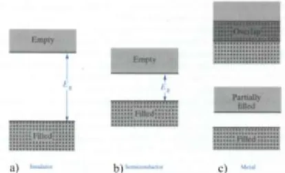
Figure 2. 6 (a) Light specularly reflecting from flat surface; (b) Multiple reflection from textured surface enhanced coupling into the material [P. Campbell 1993] ... 21 Figure 2. 7 SEM image of laser direct writing texturing features on Si substrate (a) before and (b) after etching of laser induced damage; (c) spontaneous formed Si surface features processed in vacuum with 800 nm, 100 fs pulses.(d) Square region of a Si wafer textured with spontaneously forming quasi-periodic microstructures appears black in contrast to the unprocessed regions [L. A. Dobrzanski, et al. 2008] ... 22 Figure 2. 8 Typical bands profiles at 0K for a) insulator b) semiconductor and c) metal [B. G. Streetman, et al. 1995] ... 26 Figure 2. 9 Schematic of QW band structure ... 27 Figure 2. 10 Energy level, 𝐸𝑛, and wavefunctions, 𝜑𝑛, in the infinite well [B. G. Streetman,
et al. 1995] ... 28
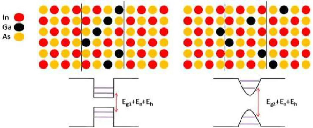
Figure 2. 11 Schematic of the band-structure and epitaxy of a non-processed vs. a QWI InGaAs/GaAs QW. ... 28 Figure 2. 12 Simulation of composition profile (a) and conduction band (b) of interdiffused In0.53/Ga0.47As/InP QW with group III and V interdiffusion with identical rates for 𝑳𝒅 =0, 10,
20, 30, 40Å. ... 29 Figure 2. 13 Point defect assisted diffusion. a) Vacancy initiated diffusion, b) an interstitial kicks an atom out of its lattice site, c) diffusion channelling through interstitial jumps [J. D. Plummer 2009]... 30 Figure 2. 14 Illustration of different point defects in a GaAs lattice. V stands for vacancy, i for interstitial for subtitutionnal, while the notation AB signifies that the atom A occupies the site of an atom B ... 31 Figure 2. 15 Valence band structure calculated for tensile, unstrained and compressive strained of InGaAs well grown on InP [A. R. Adams 2011]. ... 35 Figure 2. 16 Strain variation of identical interdiffusion v.s. interdiffusion length across a QW structure on the different positions: (a) well center (b) well close to the interface (c) barrier close to the interface (d) barrier center [H. Djie, et al. 2004]. ... 36 Figure 2. 17 View of oxygen adsorption on the InP (100). In, P, O, are indicated by brown, pink, and red spheres, respectively [K. Santosh, et al. 2013]. ... 40
xii
Figure 3. 1 Schematic of excimer laser (ArF & KrF) irradiation setup ... 50
Figure 3. 2 ArF (a) and KrF (b) laser beam profiles ... 50
Figure 3. 3 Schematic cross-section of the investigated InP/InGaAs/InGaAsP microstructure (M1580) ... 51
Figure 3. 4 Schematic cross-section of the investigated InP/InGaAsP/InGaAsP microstructure (ZJU) ... 52
Figure 3. 5 Schematic cross-section of the investigated InP/InGaAs/InGaAsP microstructure (RAC82) ... 53
Figure 3. 6 Schematic cross-section of the investigated T0808 InGaAsP/GaAs quantum well microstructure ... 53
Figure 3. 7 Photograph of RTA setup ... 54
Figure 3. 8 Typical experimental set-up for PL measurements ... 56
Figure 3. 9 Schematic of atomic force microscope... 58
Figure 3. 10 Multimode SPM ... 59
Figure 3. 11 SEM set up ... 60
Figure 3. 12 Schematic Olympus IX71 inverted microscope ... 61
Figure 3. 13 Illustration of XPS concept [B. V. Crist 2010] ... 62
Figure 3. 14 AXIS Ultra DLD XPS ... 64
Figure 3. 15 Schematic of SIMS components [I. Probe 2007] ... 67
Figure 3. 16 TOF-SIMS IV instrument... 69
Figure 3. 17 Principle of FTIR [I. Sanchonx 2011] ... 70
Figure 4. 1 AFM image of InP/InGaAs/InGaAsP irradiated by ArF laser at 82 mJ/cm2 in air ... 75
Figure 4. 2 AFM image of non irradiated and irradiated sites in by ArF laser in air after RTA ... 76
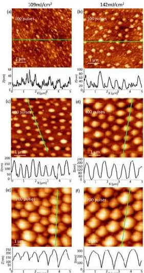
Figure 4. 3 Optical micrograph of the surface of an InP/InGaAs/InGaAsP microstructure irradiated with 400 pulses of a KrF laser at 142 mJ/cm2 (a), along with high magnification images of the central (b) and edge (c) regions. ... 80
Figure 4. 4 AFM images of the central (a) and the edge (b) regions of a site irradiated with 400 pulses of the KrF ... 81
Figure 4. 5 Microscopic images of KrF laser irradiated sites at 109 mJ/cm2 (left panel) and 142 mJ/cm2 (right panel) with 100, 400 and 700 pulses. ... 81
Figure 4. 6 AFM images and profiles along indicated lines in the central region the KrF laser irradiated sites at 109 mJ/cm2 (left panel) and 142 mJ/cm2 (right panel). ... 82
Figure 4. 7 Average height (a), size (b) and period (c) of self-organized nanostructures vs. pulse number of the KrF laser operating at 109 mJ/cm2, 124 mJ/cm2 and 142 mJ/cm2. ... 83
Figure 4. 8 PL peak intensity map and profile of the KrF laser irradiated spots with 400 pulses at 109 (a) and 142 mJ/cm2 (b). ... 85
Figure 4. 9 Normalized PL intensity of the site central region vs. pulse number when irradiated with the KrF laser at 109 mJ/cm2, 124 mJ/cm2 and 142 mJ/cm2. The inset shows PL spectra observed from the as-grown QW microstructure and the central region of the laser irradiated sites. ... 86
Figure 4. 10 AFM images and profiles along indicated lines of the central region of the ArF laser sites irradiated at 95 mJ/cm2 with (a) 400 pulses and (b) 700 pulses. ... 87
xiii
Figure 4. 11 Average size, period and height of the nano-cone structures (a) and normalized PL intensity (b) in the central region of the ArF laser irradiated sites at 95 mJ/cm2. ... 88 Figure 4. 12 AFM image of bulk InP irradiated with 400 (a) and 700 (b) pulses of the KrF laser operating at 142 mJ/cm2. ... 89 Figure 4. 13 Room temperature PL maps and microscopic pictures of a series of spots on SiO2 (50 and 150 nm thick) coated QW microstructures irradiated with ArF laser at 76
mJ/cm2... 91 Figure 4. 14 AFM image of SiO2 layer (a) and InP surface revealed after SiO2 removed (b).
The SiO2 coated as-grown material and irradiated with ArF laser at 76 mJ/cm2 underwent
RTA at 700 C for 2 min. ... 92 Figure 4. 15 Surface morphology of the InP cap layer exposed to the ArF laser radiation in the region where SiO2 was removed. ... 93
Figure 4. 16 Microscopic images of samples coated with 243 nm thick layer of SiO2 and
irradiated with KrF excimer at 124 mJ/cm2 (after RTA). ... 93 Figure 4. 17 AFM micrographs of SiO2 (a) and InP (b) layer of non irradiated sites and
irradiated sites ... 95 Figure 4. 18 High magnification InP surface morphology of irradiated sites with 25 pulses after RTA and removing SiO2 layer... 95
Figure 4. 19 The RMS roughness of the InP layer irradiated with different pulses of the KrF at 124 mJ/cm2, followed by the RTA step. The results are shown after the SiO2 layer has
been removed. ... 96 Figure 4. 20 SEM image of InP/InGaAs/InGaAsP QW sample (M1580) coated with a 243 nm thick layer of SiO2 before KrF laser irradiation (a) and after irradiated with 25 pulses at
124 mJ/cm2 (b). ... 97 Figure 4. 21 Microscopic picture of InP/InGaAs/InGaAsP microstructure coated with 40 nm (a) and 80 nm (b) Si3N4 layer after ArF laser irradiation at 70 mJ/cm2. ... 98
Figure 4. 22 AFM image of non irradiated sites and sites irradiated by ArF laser in DI water ... 98 Figure 4. 23 AFM image of non irradiated sites and sites irradiated with ArF laser in DI water and after RTA... 99 Figure 4. 24 PL map of the sample irradiated by KrF laser at 124 mJ/cm2 and RTA. ... 101 Figure 4. 25 Room temperature PL map of InP/InGaAs/InGaAsP sample coated with (a) 40 nm and (b) 80 nm Si3N4 after ArF laser irradiation and RTA. ... 101
Figure 5. 1 Si 2p (a), (d), O 1s (b), (e) and C 1s (c), (f) XPS spectra of no irradiated site and site irradiated with 25 pulses by KrF laser at 124mJ/cm2 ... 108 Figure 5. 2 In 3d 5/2 (a, b, c, d) and P 2s (e, f, g,h) XPS spectra of the SiO2 layer, SiO2-x/InP
interface 1, SiO2-x/InP interface 2 and the InP layer following KrF laser irradiation and RTA.
... 110 Figure 5. 3 XPS depth profiles of O, Si, C, In, N, P, Ga and As in non-irradiated (a) and laser irradiated (b) SiO2/InP/InGaAs/InGaAsP microstructures following their RTA. ... 112
Figure 5. 4 PL shift dependence in the InP/InGaAs/InGaAsP microstructure on the laser pulse number after (a) ArF and (b) KrF laser irradiation in air and DI water that was followed by the RTA step. ... 116 Figure 5. 5 In 3d 5/2 and P 2p XPS spectra of as grown sample (a), (d), irradiated by ArF laser at 82mJ/cm2 with 50 pulses in air (b), (e) and in DI water (c), (f). ... 118
xiv
Figure 5. 6 C 1s and O 1s XPS spectra of as grown sample (a), (d) and sample irradiated by ArF laser at 82mJ/cm2 with 50 pulses in air (b), (e) and in DI water (c), (f). ... 120 Figure 5. 7 Expanded O 1s XPS spectra of as grown sample (a) and sample irradiated by ArF laser at 82mJ/cm2 with 50 pulses in air (b) and in DI water (c)... 121 Figure 5. 8 In 3d 5/2 and P 2p XPS spectra of as grown sample (a), (d) and sample irradiated by ArF laser at 82mJ/cm2 with 50 pulses in air (b),(e) and DI water (c),(f), followed by the RTA step. ... 122 Figure 5. 9 C 1s and O 1s XPS spectra of as grown sample (a), (d) and sample irradiated by ArF laser at 82mJ/cm2 with 50 pulses in air (b),(e) and DI water (c),(f), followed by the RTA step. ... 123 Figure 5. 10 Dependence of XPS atomic concentration of InP and surface adsorbates on pulse number in the samples irradiated with ArF laser in DI water (a), in air (b) and after RTA of the sample irradiated in DI water (c) and in air (d). ... 124 Figure 5. 11 TOF-SIMS oxygen concentration depth profile in as grown sample, and in samples irradiated with ArF laser in DI water and in air before (a) and after (b) RTA at 700°C for 2 minutes. ... 126 Figure 5. 12 Dependence of XPS atomic concentration of InP and surface adsorbates on pulse number in the sample irradiated with KrF laser in DI water (a), in air (b) and after RTA of the sample irradiated in DI water (c) and in air (d). ... 127 Figure 5. 13 O 1s and In 3d XPS spectra of InOx layer coated sample before and RTA. .... 130
Figure 5. 14 In 3d 5/2 and P 2p XPS spectra of sample coated with 10 nm InOx layer
irradiated by KrF laser with 2 and 10 pulses. ... 131 Figure 6. 1 Net PL shifts dependence on RTA time ... 139 Figure 6. 2 Net blueshift amplitude dependence on the pulse number of the KrF laser at 124 mJ/cm2 and RTA (InP/InGaAs/InGaAsP QW microstructure)... 140 Figure 6. 3 SIMS profiles of O, Si, P, Ga, As and In InP/InGaAs/InGaAsP microstructure coated with a 243 nm thick layer of SiO2 after KrF laser irradiation and RTA ... 142
Figure 6. 4 Expanded view of SIMS analysis of InP/InGaAs/InGaAsP microstructure coated with 243 nm SiO2 layer after KrF laser irradiation and RTA ... 142
Figure 6. 5 Dependence of amplitude of blueshift on pulse number of samples without Si3N4
and caoted with 40 nm Si3N4 layer after ArF laser irradiation and RTA. ... 143
Figure 6. 6 Blueshift of as grown and samples coated with different thickness InOx layers
dependence on RTA temperatures ... 144 Figure 6. 7 SIMS measurement of as grown samples from M1580 microstructure before and after RTA ... 144 Figure 6. 8 SIMS results of sample coated with 40 nm InOx layer before and after RTA at 725◦C for 2 minutes ... 145 Figure 6. 9 PL shift dependence on pulse number of as grown sample (0 nm) and samples coated with 10 and 40 nm InOx layer irradiated by KrF laser at 124mJ/cm2 ... 145
Figure 6. 10 SIMS results of sample coated with 40 nm InOx layer after KrF laser irradiation
with 10 pulses and before and after RTA at 725°C for 2 minutes ... 146 Figure 6. 11 PL spectra of as grown material and sites irradiated in air (a) and DI water (b) following the RTA step. ... 151 Figure 6. 12 In 3d5/2 XPS spectra of sample irradiated by ArF laser at 82 mJ/cm2 with 50
xv
Figure 6. 13 P (—), O (---), As (—) and InO (—) intensity profiles in the microstructure after RTA of as grown sample (a) and samples irradiated by ArF laser at 82mJ/cm2 with 50 pulses in air (b) and DI water (c) investigated by ToF-SIMS... 155 Figure 6. 14 Calculated strain dependence in the 32 nm blueshifted InGaAs/InGaAsP QW region on the thickness, d, of the InOx stressing layer. ... 156
Figure 6. 15 PL map of sample (T0808) irradiated in DI water (a) and air (b) by KrF laser and RTA at 825 °C measured PLM ... 159 Figure 6. 16 PL map measured by HI-PLM of investigated sample after KrF laser QWI and RTA... 160 Figure 7. 1 PL spectra of as grown material, irradiated with 75 and 100 pulses by KrF laser at 153 mJ/cm2 in air and RTA ... 166 Figure 7. 2 PL map of the sample before KrF laser QWI. The ―1440 nm‖ signal is an arbitrary background corresponding to the region with the negligible PL emission. ... 166 Figure 7. 3 PL map (left) and PL scanning profile (right), line from A to B, of InGaAs/InP QW microstructure after KrF laser irradiation at 156 mJ/cm2 with 200 pulses through Al film mask with 40 μm x 200 μm windows and RTA at 700°C for 2 minutes. ... 167 Figure 7. 4 Detailed PL map and scanning line of small windows of InGaAs/InP QW microstructure after KrF laser irradiation at 156 mJ/cm2 with 200 pulses and RTA at 700 °C for 2 minutes ... 168 Figure 7. 5 PL map of a ZJU sample after KrF laser irradiation at 156 mJ/cm2 and RTA. Sites A and B irradiated with 75 pulses (80 nm net blue shift) and sites C and D with 150 pulses (120 nm net blue shift). ... 168 Figure 7. 6 Emission spectra (a), L-J curve (b) and I-V (c) of LD devices fabricated in the QWI (Sample 1-3) and RTA as grown sample and RTA only sample. ... 170
xvi
List of Tables
Table 2. 1. Thermal and mechanical properties of GaAs, InP and Si ... 16 Table 2. 2 Thermal properties of water, air and SiO2 ... 19
Table 2. 3 Index of CTE (α), 𝐸𝑓 and 𝜐𝑓 are the Young modulus and the Poisson coefficient, σin is the initial stress... 37
Table 3. 1 Spin-orbit splitting j values and peak area ratios. ... 65 Table 4. 1 RMS roughness on non irradiated site and irradiated sites by KrF laser in air ... 77 Table 4. 2 RMS roughness on non irradiated site and irradiated sites by ArF (I) and KrF (II) laser in DI water ... 100 Table 5. 1 Atomic percentage of elements of non irradiated sites and irradiated by KrF laser with 25 pulses ... 106 Table 6. 1 Blueshift amplitude vs. thickness of the SiO2 layer for non-irradiated QW
microstructures. ... 141 Table 6. 2 XPS P/In ratio in the as grown InP-covered InGaAs/InGaAsP/InP microstructure and ArF irradiated sites before RTA. ... 153 Table 6. 3 XPS P/In ratio in the as grown InP-covered InGaAs/InGaAsP/InP microstructure and ArF irradiated sites after 2 min RTA at 700 C. ... 153 Table 7. 1 Laser diode fabrication steps ... 168 Table A. 1 Parameters of Si used in calculation of spatial and transient temperature profiles. ... 193 Table A. 2 Atomic percentage and CA of as-received, etched and KrF laser processed Si samples with 100 and 500 pulses of 250 mJ/cm2. ... 199 Table A. 3 Atomic percentage and CA of as-received, etched and ArF laser processed Si samples with 100 and 500 pulses of 65 mJ/cm2. ... 199
1
Chapter 1 Introduction
1.1 Photonic integrated circuits
The explosive ―Moore‘s Law‖ development of integrated electronics devices along with the similarly explosive development of the Internet, has contributed to demand for communication systems providing increased bandwidth and flexibility at lower cost [R. Nagarajan, et al. 2005]. Optical communication systems can satisfy these demands, as they provide low-dispersion and low-loss (0.2 dB/km) transmission enabling higher-bit-rate and longer-distance data transport with reduced repeater spacing over that of electrical coaxial lines [G. P. Agrawal 2010]. Such systems consist of active components, used for light generation, detection, modulation and amplification, as well as passive components that serve as point-to-point links in the form of fibers or waveguides, wavelength multiplexers, wavelength demultiplexers, polarisers, isolators and switchers. A majority of present communications systems are assembled using discrete optoelectronic components as building blocks. However, there are several shortcomings with this method. The dominant optical loss is coupling loss between fiber and waveguide during communication between discrete components. The other drawback is the high cost involved with packaging discrete components separately. A reduction of the packaging cost can be accomplished by placing two or more optoelectronic chips into one package, but the device-to-device coupling issue still exists.
A new generation of high-functionality photonic integrated circuits (PICs) which combine generation, detection, modulation, amplification, switching and transport of light on a single chip can reduce power dissipation, cost and size. The monolithic integration of multiple optoelectronic devices onto a single chip eliminates the device-to-device coupling problem. Fewer packages are required as multiple components can be placed on a single chip within one package. Also, the reliability increases due to the elimination of possible mechanical movements among the elements of an optical train and the reduced driving currents allowed by the reduction in optical coupling loss between elements.
However, the integration of III-V semiconductor PICs does not develop along as the silicon-based integrated circuits (IC). There are severals factors that have contributed to this relatively
2
slow scaling of the PIC. In a PIC, there is a wide range of functions that need to be served, including light generation, amplification, modulation, detection and guiding. To optimize performance of each function, different material structures are likely required in the different components serving these functions. This is a difficult task for the common 2-dimensional growth and processing platforms used for device fabrication. This means that after the first growth, lithography and etching steps are applied on the sample before putting it back in the epitaxial reactor to make a second growth. Since growth processes are long, and the etching treatments can generate a considerable amount of defects at the surface and edges of the wafer, such a technique can be expensive with low production rates. The defects embedded in the interfaces formed during etching procedures often cannot be removed during the consecutive growth and they become responsible for diminishing quality of the devices [R. Nagarajan, et al. 2005, M. Smit, et al. 2007]. The growth techniques developed for multibandgap engineering include butt-joint regrowth, selective area growth, offset quantum wells and dual quantum wells [E. J. Skogen, et al. 2005]. Besides the common drawbacks discussed before, butt-joint regrowth has a difficulty in achieving high-quality interface that would avoid reflections and losses in axial waveguides [J. Binsma, et al. 1997]. The selective area growth technique is less flexible to achieve multibandgap wafer [B. Mason, et al. 1998]. The offset quantum wells and dual quantum wells approach suffers from limited quantities bandgaps on one platform [M. Aoki, et al. 1993]. Consequently, quantum well intermixing (QWI) has been investigated as one of the most promising approaches for the cost-effective fabrication of PICs [W. Laidig, et al. 1981, J. H. Marsh 1993, E. J. Skogen, et al. 2005, S. B. Estrella, et al. 2012]. It allows for the strategic, post growth, tuning of the quantum well (QW) band edge by inducing atomic interdiffusion between the well and barrier materials. This technique enables the generation of multiple QW bandgap on a chip without difficult growths steps or discontinuities in axial waveguide. QWI offers more design flexibilities than the offset QW method [B. Mason, et al. 1998] and offers a simpler fabrication scheme than the butt-joint regrowth method [J. Binsma, et al. 1997] or selective area growth method [M. Aoki, et al. 1993]. The known methods of QWI include impurity induced intermixing [W. Laidig, et al. 1981], impurity-free vacancy diffusion [J. Teng, et al. 2002], ion implantation induced QWI [V. Aimez, et al. 2002], and visible [J. Epler, et al. 1986], IR [B. S. Ooi, et al. 2004] and UV [J. J. Dubowski 2003] laser induced QWI. QWI obtained by annealing
3
of selective area coated QW wafers with different oxides, nitrides and fluorides (fabricated by conventional thin film deposition techniques) has also been investigated [P. Deenapanray, et al. 2002, A. Francois, et al. 2006].
To illustrate the QWI use in PICs application, scientists have first fabricated and studied external cavity laser diodes with integrated passive waveguides generated by impurity induced disordering in 1992 [S. Andrew, et al. 1992]. Then, high performance devices fabricated in QWI material, e.g. widely tunable, negative chirp, 10 Gb/s transmitter, sampled grating distributed Bragg reflector (SG-DBR) laser and electro absorption modulator (EAM) on QWI platform [E. J. Skogen, et al. 2005]. The band-edge of the EAM can be blue-shifted by QWI such that it maintains a high absorption coefficient, reasonable insertion loss and without severe degradation to the exciton peak. The passive component band-edge can be further blue-shifted for minimum loss [E. J. Skogen, et al. 2005]. Plasma bonding techniques have been used to bond the integrated laser-EAM device with already patterned tuned bandgap on to patterned SOI (silicon-on-insulator) substrate, as shown in Figure 1.1. Four bandgaps were generated on a single chip and used to realize a multi-channel distributed feedback (DFB) laser array and lasers-EAM modulators. A 150 µm long taper following the EAM is used to transit the optical mode from the III-V semiconductor to the Si. Thirteen CW operational lasers with 40-70 mA threshold current and four-channel laser-EAM arrays with 2 GHz bandwidth were fabricated [S. Jain, et al. 2011].
4
Characterization of intermixed material has typically been carried out by measuring optical properties of the intermixed material and photonic devices fabricated on the intermixed platforms [J. H. Marsh 1993, E. Li 2000]. Photoluminescence (PL) has frequently been employed to investigate QW bandgap modification and provides information about surface and interface modification/damage during the intermixing step [J. H. Marsh 1993]. The measurement of the laser diode threshold current increment also provides the information about the density of defects and modified quantum confinement in the intermixed active region [V. Aimez, et al. 2002]. To measure the atom or defect diffusion inside the QW microstructure, secondary ion mass spectroscopy (SIMS) was used to compare atomic profile depths of QW before and after QWI [J. Teng, et al. 2002]. In order to reduce the damage of the active region of QW in the intermixing, many studies focus on creating surface defects by means of capped stressor layers and low energy ion implantation. High resolution X-ray photoelectron spectroscopy (XPS) has been used to analyse the surface defects creation on non-stoichemical InP surface during ion induced QWI [C. Xu, et al. 2009]. In addition, XPS can also be used to study the indepth atom diffusion profile of QW [P. Deenapanray, et al. 2002, S. Barik, et al. 2007]. As the surface and interface morphology modification is directly related to these chemical modifications, the surface morphology investigation with atomic force microscope (AFM) and scanning electron microscope (SEM) can be used to verify the surface defect generation and diffusion process [D. G. Deppe, et al. 1988, J.-S. Lee, et al. 1998].
1.2 UV laser QWI
Despite significant advancements, QWI technology has remained the subject of ongoing investigation triggered, e.g., by the lack of precision in achieving targeted amplitudes of bandgap shifting, and it has suffered from unintentionally introduced impurities present on the surface of processed wafers. Such impurities could influence the QWI amplitude attempted with ion implantation, plasma exposure or with layers of different oxides, nitrides, fluorides, etc. Uncontrolled presence of impurities will also lead to the reduced quality of the QWI material and compromised performance of devices made from such material. In that context, the application of a strongly absorbed UV laser radiation for surface modification of III-V QW microstructures offers the possibility to investigate the role of surface impurities and that of chemical
5
composition of a laser-fabricated layer, typically thinner than 10 nm, in the QWI process. The UV laser QWI approach (UV-QWI), originally discussed in [J. J. Dubowski 2003], employs an excimer laser (= 248 nm) to alter the near-surface region (~10 nm) of the QW microstructure, as shown in Figure 1.2. The goal of this step is to create a ―reservoir‖ of defects at the surface of a QW microstructure. Another form of the alteration could be chemical in nature, resulting from the irradiation in different environments. Processing with shaped UV laser beams, or using a mask projection technique, provides a direct method to achieve selective area processing required for manufacturing of PIC. Following the UV laser exposure, the QW microstructure needs to be annealed at a temperature sufficient to drive defects from the reservoir into the vicinity of the QW region where the intermixing (between well and barrier material) will take place. This step is carried out in a rapid thermal annealing (RTA) oven. In addition to driving impurities and/or point defects towards the QW region, typically located less than 2 m below the surface, the high-temperature treatment could change the chemical composition of the laser-fabricated layer and induce/reduce stress in the QW region related to the presence of such a layer. Excimer laser has already been employed in the microelectronics industry for high resolution optical lithography. Thus, these tools could be relatively easily accommodated for industrial processes involving QWI.
Figure 1. 2 UV or excimer laser irradiation of a QW heterostructure allows selective area QWI [J. J. Dubowski 2003]. UV laser QWI is applicable in both InP and GaAs based QW and QD microstructures. In InP based QWs microstructures, the UV-QWI process is based on the localized generation of point defects through UV laser pulse absorption. The excess concentration of point defects promotes intermixing between the barriers and wells during the annealing step. The blueshift strongly depends on the fluence and pulse number. A phenomenological model was developed to fit the
6
wavelength shift dependence up to 125 nm, which indicates that UV laser QWI technique is more efficient in defect generation than pulsed laser induced QWI [J. Genest, et al. 2008a]. Excimer laser QWI was also reported to induce significant blueshifts due to laser modification of surface chemistry of InP cap material irradiated in various environments, including air, DI water and dielectric layer coating [N. Liu, et al. 2011a, N. Liu, et al. 2013]. In GaAs based QW microstructure, the UV laser QWI process leads to the suppression of intermixing in InAlGaAs/AlGaAs/GaAs and AlGaAs/GaAs heterostructures due to stress from surface oxides initiated by UV laser irradiation and developed during the RTA step [J. Genest, et al. 2007a]. The short wavelength of the surface modifying laser radiation and the relatively shallow location of the QW allow suppression of QWI with a spatial resolution as high as 1 μm [J. Genest, et al. 2007b]. Thus, excimer laser has the potential to offer a highly efficient and controllable method of QWI.
1.3 Project description
The goal of the project was to investigate the role of excimer lasers in fabricating high-quality QWI material. The QW microstructures material mainly studied in this project are InP/InGaAs/InGaAsP microstructures with QW active region below surface cap layer around 76 nm or 1.5 µm. As dielectric layers of SiO2 and Si3N4 are popular in semiconductor optoelectronic
devices fabrication, we have studied properties of InP/InGaAs/InGaAsP microstructure coated with such layers and irradiated with an excimer laser before RTA. Furthermore, deionized water (DI) environment is known to be chemically ―simple and clean‖ that could reduce the uptake of contamination of air environment during laser irradiation. For that reason, it was interesting to investigate if UV laser QWI by irradiating QW wafers in DI water environment could lead to the fabrication of the QWI material with improved optical properties. In our preliminary studies, we also found that UV laser created indium oxide (InOx) played an important role in the QWI
process. Following this lead, in this thesis I have investigated the QWI effect in QW microstructures coated with InOx and irradiated with excimer laser. As the surface defects
generation and surface chemical and morphology alteration could depend on the energy of laser emitted photons, two different wavelengths excimer lasers, ArF and KrF lasers, were used in this research. In addition, both InP (full and partially laser diode QW) and GaAs (partially laser diode
7
QW) based QW microstructures were investigated. The surface and interface formation during excimer laser irradiation and annealing were mainly measured by AFM. The surface and interface chemical modifications and atoms diffusions during process were characterized by surface XPS, indepth XPS and SIMS. The optical properties of all the QW microstructures after UV laser QWI were mainly characterized by PL measurements as well as by investigating luminescence quality from laser diodes fabricated in the intermixed full laser diode QW microstructures.
In summary, this thesis was addressed to study the mechanism of excimer laser QWI in III-V semiconductor microstructures and propose a novel controllable UV laser QWI recipe leading to the fabrication of high quality wafers required in the fabrication of PICs.
1.4 Contribution of this research
1.4.1 Excimer laser induced QWI in InP/InGaAs/InGaAsP microstructures coated with different dielectric layers
Liu, N., Moumanis, Kh., and Dubowski, J. J. ArF excimer laser-induced quantum well
intermixing in dielectric layer coated InGaAs/InGaAsP microstructures, 4th Pacific
International Conference on Applications of Lasers and Optics (PICALO), Wuhan, China, March 23-25, 2010, PICALO 2010 Conference Proceedings, ISBN:978-0-912035-56-7, article number: M404, (2010);
Liu, N., Moumanis, Kh., and Dubowski, J. J. Surface morphology of SiO2 coated
InP/InGaAs/InGaAsP microstructures following irradiation with the ArF and KrF excimer lasers, Photonics West Conference: Laser Application in Microelectronic and
Optoelectronic Manufacturing (LAMOM) XVI, San Francisco, USA, January 22-27, 2011, (Oral Presentation), Proceeding of SPIE, Vol. 7920, 7920C, (2011);
Liu, N., Blais, S. and Dubowski, J. J. Surface and interface study of SiO2-x coated
InP/InGaAs/InGaAsP semiconductor laser microstructures processed in the soft KrF laser irradiation regime, Pacific RIM Laser Damage 2011: Optical Materials for High
Power Lasers, Shanghai, China, November 6-9, 2011, Proceeding of SPIE, Vol. 8206, 820609, (2012);
8
1.4.2 UV laser QWI of InP/InGaAs/InGaAsP microstructures irradiation in air and DI water
Liu, N., Moumanis, Kh., Blais, S. and Dubowski, J. J. : XPS study of
InP/InGaAs/InGaAsP microstructures irradiated with ArF laser in air and deionized water, Photonics West Conference: Synthesis and Photonics of Nanoscale Material IX,
San Francisco, USA, January 21-26, 2012, Proceeding of SPIE, Vol. 8245, 82450E, (2012);
Liu, N. and Dubowski, J. J.: Chemical evolution of InP/InGaAs/InGaAsP microstructures
irradiated in air and deionized water with ArF and KrF lasers, Applied Surface Science
270, 13, 16-24, (2013);
Liu, N., Poulin S. and Dubowski, J. J.: Enhanced photoluminescence from UV laser
quantum well intermixed InGaAs/InGaAsP/InP laser microstructures, Journal of Physics
D: Applied Physics, 46, 445103, (2013);
Liu, N., Moumanis, Kh., and Dubowski, J. J.: Self-organized Nano-cone Arrays in InP/InGaAs/InGaAsP Microstructures by Irradiation with ArF and KrF Excimer Lasers,
Journal of Laser Micro/Nano Engineering 7, 2,130-136, (2012);
1.4.3 Application of excimer laser QWI for photonic device fabrication
Béal, R., Liu, N. Moumanis, Kh., Aimez, V. and Dubowski, J.J. Multi Section Bandgap
Tuned Superluminescent Diodes Fabricated by UV Laser Induced Quantum Well Intermixing, International Conference on Information Photonics (IP), Ottawa, Canada,
May, 2011, IEEE Proceeding of IP2011, ISBN: 978-1-61284-315-5, article number:
5953731, (2011);
Kaleem, M., Zhang, X., Zhuang, Y., He, J.J., Liu, N., and Dubowski, J. J. UV laser
induced selective-area bandgap engineering for fabrication of InGaAsP/InP laser devices, Optics & Laser Technology 51, 36-42, (2013);
9
Liu, N., Hassen W. and Dubowski, J.J.: Excimer laser assisted chemical process for
formation of hydrophobic surface of Si (001), Applied Physics A, (published on line),
DOI: 10.1007/s00339-014-8380-9, (2014);
Liu, N, Huang X. and Dubowski, J.J.: Selective area in situ conversion of hydrophobic to hydrophilic surface of Si by excimer laser irradiaiton in hydrogen peroxide, Journal of Physics D: Applied Physics, (submitted);
1.4.5 XPS and AFM analysis of semiconductor surfaces (My contribution was to the
semi-quantitative analysis of XPS data and collection of AFM images)
Arudra, P., Marshall, G. M., Liu, N., and Dubowski, J. J. :Enhanced Photonic Stability of
GaAs in Aqueous Electrolyte Using Alkanethiol Self-Assembled Monolayers and Postprocessing with Ammonium Sulfide, Journal of Physical Chemistry C116, 2891-2895,
(2012);
Huang, X., Liu, N., Moumanis, Kh., and Dubowski, J. J.: Water-Mediated Self-Assembly
of 16-Mercaptohexadecanoic acid on GaAs(001), Journal of Physical Chemistry C117,
1590-1597, (2013).
1.5 Thesis structure
The topics of the remaining eight chapters of the current thesis are as following:
Chapter 2: covers the concepts of laser-matter interaction, including laser induced surface temperature, morphology and chemical modification; discusses the principle of QW and QWI and the role of strain and point defects in the QWI process;
Chapter 3: presents excimer laser irradiation setups; introduces the investigated semiconductor microstructures and discusses characterization techniques used during my work;
Chapter 4: discusses UV laser induced InP/InGaAs/InGaAsP microstructure surface morphology modification in air and presents self-organized nanocone structures created outside of QWI laser parameters and its effect in PL intensity enhancement; discusses surface morphology of microstructure coated with dielectric layers (SiO2 and Si3N4) and in DI water;
10
Chapter 5: XPS analysis of chemical evolution of InP/InGaAs/InGaAsP microstructure after ArF and KrF laser irradiation in air and DI water; XPS analysis of surface and interface of the microstructure coated with SiO2 and InOx layer during KrF laser QWI;
Chapter 6: summarizes the PL shift dependence on laser parameters when irradiated in the discussed environments, including in air, DI water and dielectric layers (SiO2, Si3N4 and InOx)
coated; SIMS analysis of atoms diffusion of the interface of InP/InGaAs/InGaAsP microstructure after UV laser QWI in air and DI water and studies the atoms diffusion influence on PL shift and PL intensity of intermixed microstructures; SIMS analysis of atoms diffusion in UV laser QWI in the other different environments;
Chapter 7: investigates laser diode fabrication on KrF laser QWI material; KrF laser QWI on GaAs based QW and measured with a novel HI-PLM setup developed by our group;
Chapter 8: presents the conclusion of this thesis and future direction for the project.
Appendix: discusses UV laser induced Si wettability modification, including excimer laser induced selective area hydrophilic Si surface by irradiation in hydrogen peroxide and hydrophobic surface by irradiation in methanol solution.
1.6 Bibliography
Agrawal, G.P.: (2010), Fiber-optic communication systems (Wiley), 587p.
Aimez, V., Beauvais, J., et al., (2002), Low-energy ion-implantation-induced quantum-well intermixing, IEEE Journal of Selected Topics in Quantum Electronics, vol. 8, no4, 870-879. Andrew, S., Marsh, J., et al., (1992), Quantum-well laser with integrated passive waveguide fabricated by neutral impurity disordering, IEEE Photonics Technology Letters, vol. 4, no5, 426-428.
Aoki, M., Suzuki, M., et al., (1993), InGaAs/InGaAsP MQW electroabsorption modulator integrated with a DFB laser fabricated by band-gap energy control selective area MOCVD, IEEE
Journal of Quantum Electronics, vol. 29, no6, 2088-2096.
Barik, S., Fu, L., et al., (2007), Impurity-free disordering of InAs/ InP quantum dots, Applied
11
Binsma, J., Thijs, P., et al., (1997), Characterization of butt-joint InGaAsP waveguides and their application to 1310 nm DBR-type MQW gain-clamped semiconductor optical amplifiers, IEICE
transactions on electronics, vol. 80, no5, 675-681.
Deenapanray, P., Gong, B., et al., (2002), Impurity-free disordering mechanisms in GaAs-based structures using doped spin-on silica layers, Applied Physics Letters, vol. 80, 4351.
Deppe, D.G., and Holonyak, N., (1988), Atom diffusion and impurity induced layer disordering in quantum well III-V semiconductor heterostructures, Journal of applied physics, vol. 64, no12, R93-R113.
Dubowski, J.J.: ‗Laser-induced bandgap shifting for photonic device integration‘, US Patent 6,514,784, 2003.
Epler, J., Burnham, R., et al., (1986), Laser induced disordering of GaAs AlGaAs superlattice and incorporation of Si impurity, Applied Physics Letters, vol. 49, 1447.
Estrella, S.B., Johansson, L.A., et al., (2012), Widely Tunable Compact Monolithically Integrated Photonic Coherent Receiver, IEEE Photonics Technology Letters, vol. 24, no5, 365-367.
Francois, A., Aimez, V., et al., (2006), Enhancement of quantum well intermixing on InP/InGaAs/InGaAsP heterostructures using titanium oxide surface stressors to induce forced point defect diffusion, Applied Physics Letters, vol. 89, 164107.
Genest, J., Dubowski, J.J., et al., (2007a), Suppressed intermixing in InAlGaAs/AlGaAs/GaAs and AlGaAs/GaAs quantum well heterostructures irradiated with a KrF excimer laser, Applied
Physics A: Materials Science & Processing, vol. 89, no2, 423-426.
Genest, J., Dubowski, J.J., et al., (2007b), UV laser controlled quantum well intermixing in InAlGaAs/GaAs heterostructures, Journal of Physics: Conference Series, vol. 59, 605-609. Genest, J., Beal, R., et al., (2008), ArF laser-based quantum well intermixing in InGaAs/InGaAsP heterostructures, Applied Physics Letters, vol. 93, 071106.
Jain, S., Sysak, M., et al., (2011), Integrated hybrid silicon DFB laser-EAM array using quantum well intermixing, Optical express, vol. 19, no14, 13692-13699.
Laidig, W., Holonyak, N., et al., (1981), Disorder of an AlAs/GaAs superlattice by impurity diffusion, Applied physics letters, vol. 38, no10, 776-778.
Lee, J.-S., Ren, H.-W., et al., (1998), InGaAs quantum dot intermixing and evaporation in GaAs capping layer growth, Journal of applied physics, vol. 84, 6686.
12
Liu, N., Blais, S., et al., (2011), Surface and interface study of SiO2-x coated
InP/InGaAs/InGaAsP semiconductor laser microstructures processed in the soft KrF laser irradiation regime, Proceeding of SPIE, vol. 8206, 820609.
Liu, N., and Dubowski, J.J., (2013), Chemical evolution of InP/InGaAs/InGaAsP microstructures irradiated in air and deionized water with ArF and KrF lasers, Applied Surface Science, vol. 270, no13, 16-24.
Marsh, J.H., (1993), Quantum well intermixing, Semiconductor Science and Technology, vol. 8, no6, 1136.
Mason, B., Fish, G.A., et al., (1998), Ridge waveguide sampled grating DBR lasers with 22-nm quasi-continuous tuning range, IEEE Photonics Technology Letters, vol. 10, no9, 1211-1213. Nagarajan, R., Joyner, C.H., et al., (2005), Large-scale photonic integrated circuits, IEEE
Journal of Selected Topics in Quantum Electronics, vol. 11, no1, 50-65.
Ooi, B.S., Ong, T.K., et al., (2004), Multiple-wavelength integration in InGaAs-InGaAsP structures using pulsed laser irradiation-induced quantum-well intermixing, IEEE Journal of
Quantum Electronics, vol. 40, no5, 481-490.
Skogen, E.J., Raring, J.W., et al., (2005), Monolithically integrated active components: a quantum-well intermixing approach, IEEE Journal of Selected Topics in Quantum Electronics, vol. 11, no2, 343-355.
Smit, M., Bente, E., et al., (2007), Current status and prospects of photonic IC technology, IEEE
19th International Conference on Indium Phosphide & Related Materials, 2007 (IPRM'07),
IEEE, 3-6
Teng, J., Dong, J., et al., (2002), Controlled group V intermixing in InGaAsP quantum well structures and its application to the fabrication of two section tunable lasers, Journal of Applied
Physics, vol. 92, 4330.
Xu, C., and Mei, T., (2009), Inductively Coupled Argon Plasma-Enhanced Quantum-Well Intermixing: Cap Layer Effect and Plasma Process Influence, IEEE Journal of Quantum
13
Chapter 2 Background information
In this chapter, first I review the fundamental laser material interaction. I discuss laser induced surface temperature, morphology and chemical modification of materials. The focus is on mechanisms of UV laser interaction with semiconductor surfaces. I also discuss the band structure of QW, the principle of QWI and the influence of defects and mechanical strain on the QWI effect.
2. 1 Laser-matter interaction
The interaction mechanism between laser light and material depends on the parameters of laser beam and properties of the material. Laser parameters contain laser wavelength, intensity, spatial and temporal coherence, polarization, angle of incidence and irradiation time (e.g. pulse width and number of pulses for pulse laser). The material is characterized by its chemical composition and physical microstructures, which determines the type of elementary excitations and interactions between them. Laser processing can be classified into two groups, at least in principle : conventional laser processing and laser chemical processing [D. Bauerle 2010]. Conventional laser processing can be performed in an inert atmosphere and takes place without any changes in the overall chemical composition of the material being processed. Laser chemical processing is characterized by overall change in the chemical composition of material or the activation of a chemical reaction, as well as morphological changes in the surface and near surface region.
When laser beam irradiates the surface of a material, a fraction of laser beam is reflected; the penetrating radiation is absorbed inside the bulk material where the intensity decreases for linear absorption corresponding to Beer‘s law [R. F. Haglund, et al. 1997]:
𝐼 𝑥 = 1 − 𝑅 𝐼0𝑒(−𝛼𝑥 ), (2. 1)
where 𝐼0is intensity at surface at x=0, 𝛼 is absorption coefficient and 𝑅 is reflectance.
The inverse of the absorption coefficient (𝛼) can be regarded as the optical penetration depth, which is the depth where the intensity has fallen to 1/e of the incoming value. Both 𝛼 and 𝑅 are important in a laser irradiation process, but they can vary with laser wavelength and material
14
composition. Figure 2.1 (a) and (b) shows the 𝑅 and 𝛼 of Si, GaAs and InP as a function of photon energy extracted from [H. Philipp, et al. 1963, S. S. Vishnubhatla, et al. 1968, D. E. Aspnes, et al. 1983, D. Smith, et al. 1985]. For the photon energy exceeding the bandgap, 𝛼 increases rapidly to around 106-107 cm-1, so the penetration depth of Si, GaAs and InP is very shallow. However, heat diffusion processes can spread laser generated defects to depths significantly exceeding those of the penetration depth α-1. Note that the InP absorption at 248 nm (1.78 x 10⁶ /cm) is slightly stronger than that at 193 nm (1.28 x 10⁶ /cm). Thus, for a comparable reflection of this material at 193 and 248 nm, it is expected that the KrF laser radiation would be absorbed in shallower layer than that of the ArF laser.
Figure 2. 1 Reflectance (𝑅) and absorption (𝛼) and and of GaAs, InP and Si as a function of incident light photon energy extracted from reference [H. Philipp, et al. 1963, S. S. Vishnubhatla, et al. 1968] and [D. E. Aspnes, et al. 1983, D. Smith, et al.
1985]
2.1.1 Laser induced temperature estimation
The primary effect of an intense laser pulse absorbed into a solid material with high absorption is heating of the surface layer to relatively high temperatures in only a few nanoseconds. The most important parameters in understanding thermal effects are the temperature distribution in the material and its development in time. Reasonable estimates of the surface temperature distribution can be made from solution to the thermal diffusion equation:
𝑄 − ∇(𝑘(𝑇)∇𝑇) = 𝜌𝐶𝜕𝑇 𝜕𝑡
(2. 2)
15
𝑄 = 1 − 𝑅 𝛼𝐹𝑃 𝑡 𝑒−𝛼𝑧𝐺(𝑟) (2. 3)
where 𝜌: material density; 𝐶 : specific heat; 𝑘 : thermal conductivity; 𝐹 : laser fluence; P(t): temporal pulse shape ( 𝑃(𝑡)𝑡
ℓ 𝑑𝑡
∞
0 = 1), 𝑡ℓ is the pulse duration; G(r): spatial laser beam shape, e.g.
circular Gaussian beam is 𝐺 𝑟 = exp −2𝑟2
𝑤02 ; w0: beam waist at the sample; r: beam radius coordinate; z: direction into the material; T and t: temperature and time, respectively. Although exact calculations have suffered from the problems of temperature dependent physical parameters that often are not easily predicated, good agreements between experiment and calculation are obtained when defining parameters function from experiments [R. F. Haglund, et
al. 1997].
The boundary condition in the heat transfer process is as follows:
𝑞0− 𝑇𝑖𝑛𝑓 − 𝑇 + 𝐶𝑜𝑛𝑠𝑡 𝑇𝑎𝑚𝑏4− 𝑇4 = 𝑘∇𝑇 (2. 4)
Where 𝑞0: inward flux; : heat transfer coefficient; 𝑇𝑖𝑛𝑓: temperature far away from the modeled domain; 𝑇𝑎𝑚𝑏 : ambient temperature (heat radiation); 𝐶𝑜𝑛𝑠𝑡 : Emissivity·sigma (Stefan Boltzman‘s heat radiation constant).
Numerical techniques such as finite difference or elemental analysis are required and succeeded to solve these equations [Radoslaw Stanowski, et al. 2006]. In most cases, there are assumptions that can be applied to simplify analytic solutions, e.g. treating material properties independent of T. In this project, commercial finite element method (FEM) software, (COMSOL group), was used to solve the heat transfer partial differential equation and calculate temperature temporal and spatial profiles. The FEM approach takes advantage of the finite element discretization of the calculated model‘s geometry into mesh elements. The properties of adjacent elements in the nodes of the generated net are shared during progressive iteration steps, so the energy flux phenomena could be calculated for, e.g. diffusion or heat transfer. The FEM method (Comsol software) allows generating mesh elements of various sizes and shapes, depending on the calculated physical process. The size of mesh elements is not only a critical factor for accuracy of the calculated results, but also it affects the total time of calculations. To simplify the calculations, we assumed that the irradiated samples are of circular shape. This allowed us to use a 2D model employing circular axial symmetry to investigate temperature modification in depth
16
of the microstructures (r-z). Calculations were carried out to determine the temporal temperature behavior in the middle of the laser irradiated spot as well as both spatial temperature profiles. The laser spot was situated in the center axis of the model‘s geometry. After designing the multilayer geometrical microstructure, the main material properties parameters in the above equations were defined in the software using the values in Table 2.1.
Table 2. 1. Thermal and mechanical properties of GaAs, InP and Si
GaAs InP Si
𝑘 0.425* (300/T) 0.68 (T=300) 1.3
𝜌 (g/cm3) 5.31 4.81 2.329
𝐶 (J/g.K) 0.303+0.015 *(T/300) 0.31 (T=300) 0.7
*Tmelt (K) 1520 1333 1680
*Tmelt is the material melting temperature.
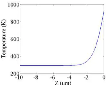
Figure 2.2 shows the geometry model of InP sample during KrF laser irradiation in air. In this model, (0, 0) is the laser spot center on the InP surface and the laser beam direction is along minus Z direction. The circular laser pulse duration is 23 ns, and repetition rate is 2 Hz. The circle laser spot size and sample size are rlaser = 0.75 x 10⁻³ m and rInP = 2.5 x 10⁻³ m.
Figure 2. 2 Geometry model (Temperature profile) of InP sample during KrF laser irradiation in air at 124 mJ/cm2
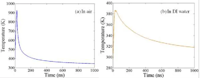
As the reflectance depends on laser wavelength, the heat source absorbed by the sample was comparable when it was irradiated by KrF laser at 124 mJ/cm2 (R 0.6) and by ArF laser at 82 mJ/cm2 (R 0.43). Here we take KrF laser irradiation at 124 mJ/cm2 as an example for
![Figure 1. 1 Top view of a PIC chip fabricated on the Si platform [S. Jain, et al. 2011]](https://thumb-eu.123doks.com/thumbv2/123doknet/5422290.126788/21.918.162.774.702.1020/figure-view-pic-chip-fabricated-si-platform-jain.webp)