O
pen
A
rchive
T
OULOUSE
A
rchive
O
uverte (
OATAO
)
OATAO is an open access repository that collects the work of Toulouse researchers and
makes it freely available over the web where possible.
This is an author-deposited version published in :
http://oatao.univ-toulouse.fr/
Eprints ID : 18274
To link to this article :
DOI: 10.1109/EMCEurope.2017.8094670
URL :
http://dx.doi.org/10.1109/EMCEurope.2017.8094670
To cite this version : Hairoud Airieau, Siham and Dubois, Tristan and
Duchamp, Geneviève and Durier, André An Analog-to-Digital Converter
Immunity Modelling based on a Stochastic Approach. (2017) In: EMC Europe
2017, 4 September 2017 - 8 September 2017 (Angers, France).
Any correspondence concerning this service should be sent to the repository
administrator:
[email protected]
Abstract—This paper deals with the immunity study of a 12-bits
SAR (Successive Approximation Register) Analog-to-Digital converter from Analog Devices facing to an EM (ElectroMagnetic) disturbance. The RF (Radio Frequency) disturbances are injected through the Vdd pin of the studied
component and its behavior is modeled. Due to the dispersion of conversion results, the approach proposed here is based on a stochastic modeling. The identification of the statistical distributions, describing the behavior of the disturbed component, is performed using the Akaike information criterion. Modeling results are compared to DPI (Direct Power Injection) measurements.
Index Terms—A/D converter, EMC/EMI, CDF (Cumulative
Density Function), IB (Immunity Behavioral), DPI (Direct Power Injection), PDF (Probability Density Function), Stochastic process.
I.! INTRODUCTION
HE automotive, avionic and military industries face a significant dilemma arise by the continuous and fast evolution of integrated circuit manufacturing processes. As a consequence of that progress, once an IC is no longer manufactured, the embedded system that uses it becomes obsolete. Today, the electronic parts that compose a product have a life cycle that is significantly shorter than the life cycle of the product. To face that problem, many obsolescence mitigation approaches are proposed. The two most common approaches, followed by the industrials, consist in buying and storing or multi-sourcing.
The first method, although costly (inventory management), is not necessarily efficient. The issue here is related to the storage conditions which can impair the performance of the integrated circuits. Indeed, the storage conditions can modify the components features during the time. The second method consists in use of components with identical shape fit and function using newer technologies.
But, in all cases from an EMC (ElectroMagnetic Compatibility) point of view, these methods are not sufficient to insure the functionality and EMC compliance of the final system. This is why industrials are seeking for new methods to
anticipate EMC/EMI (ElectroMagnetic
Compatibility/Electromagnetic Interferences) related to COTS (Commercial Off-The-Shelf Products) issues, and so avoid
additional production costs. One of the solution is to develop predictive models which will be used in simulation tools to ensure long term EMC compliance of electronic equipment (emissivity, immunity) [1-2]. These models can be electrical in order to be used in electrical simulator as Spice, ADS, Multisim or can be behavioral in order to be used in simulator like Matlab or Simplorer which can use VHDL-AMS descriptions for example [3-10].
The aim of this paper is to present the methodology to determine a behavioral model of an Analog-to-Digital converter from Analog Devices face to an EM disturbance. In this study, we consider a black box modeling approach, where the electromagnetic disturbances are described by pure mathematical models with strong abstraction level.
Here, the immunity of this IC against the EM disturbances is calculated thanks to a stochastic modeling approach. The key motivation for this work is the non-deterministic nature of the conversion results given by the component under test and the dispersion range due to accuracy [9-10]. Moreover, the model is developed and validated thanks to DPI (Direct Power Injection) measurements. The simulated and measured immunity levels are then compared and analyzed.
After a brief description of the considered DUT and PCB in section II, section III introduces the immunity study and the measurement setup used to extract the influent parameters. Then section IV presents the study of the component behavior on nominal conditions. Section V presents in details the approach followed to develop and to validate the immunity model. The conclusions and perspectives are finally exposed in section VI.
II.! DESCRIPTION OF THE DEVICE UNDER TEST AND THE
DEMONSTRATOR
This part of the paper gives an overview of the considered device under test and the electronic board used as demonstrator.
A.! Analog-to-digital converter characteristics
The tested component is the AD7476 from Analog Devices. It is a high speed, low power and successive approximation Analog-to-Digital Convertor (ADC). The conversion process and data acquisition are controlled using a SPI (Serial Peripheral Interface) communication interface. Table 1 summarizes some of its characteristics.
An Analog-to-Digital Converter Immunity
Modeling based on a Stochastic Approach
S . HAIROUD AIRIEAU1,2, T. DUBOIS1, G. DUCHAMP1, A. DURIER2
1 Univ. Bordeaux Lab. IMS, 351 Cours de la Libération, 33400 Talence, [email protected] 2 IRT Saint Exupery, 118 Route de Narbonne, 31432 Toulouse, [email protected]
B.! Demonstrator characteristics
The component is mounted on the PCB presented in Fig. 1. The tested board has four layers with an overall thickness equal to 1.6 mm. The material used is the standard FR4 epoxy.
III.! IMMUNITY STUDY AND MEASUREMENT SETUP A.! Immunity modelling
The study and behavioral modelling of a component's immunity conventionally comprises two parts [5-7], [9-10]. The first corresponds to the determination of the coupling paths by which the perturbation is transmitted to the sensitive part of the component and the second consists in evaluating the behavior of the sensitive core. Finally, the model output is compared to an application-dependent user-definable threshold.
The present paper is focused on the modeling of the active part of the device in order to characterize the device dysfunction due to electromagnetic disturbance. The model output should describe the IC behavioral response to a disturbing signal.
B.! DPI measurement setup
The DPI (Direct Power Injection) measurements were carried out by injecting an interference signal through a bias tee connected to one of IC pins as presented in Fig. 2. Here, we will focus on injecting interferences only through the Vdd
pin (power supply pin of the ADC). This injection of interferences through Vin (voltage to be convert by the ADC)
has been performed but will not be presented in this paper.
As in classical DPI tests, we have to quantify the power that induces the device under test dysfunction. The power Ptrans
absorbed by the tested component is considered as a relevant parameter to characterize the signal drift at the observable output. It is deduced from forward and reverse powers (Pforw
and Prev, respectively) as shown by Eq. (1).
Note that Pforw and Prev are measured from the bidirectional
coupler with a power meter (see Fig. 2). IV.! STUDY OF THE AD7476 IN STATIC MODE
Before injecting the RF disturbances through different pins of the ADC, we study the influence of Vdd and/or Vin on the
conversion results under nominal conditions.
The test performed here consists in making N conversions for different pairs of values (Vdd, Vin). The decimal value of the
conversion result can be calculated from Eq. (2).
Where E means the integer part. From this equation, it is possible to recalculate (Vout) using Eq. (3).
The effect of the interferences will be observed by comparing
Vout to Vin. According to the datasheet Vout should at most be
equal to Vin ± 1 LSB. This 1 LSB “error” is due to the intrinsic
operation of the component. Note that the LSB (Least Significant bit) size for the AD7476 is Vdd /4096 and it is
considered as the smallest possible variation of the output voltage. According to the datasheet of the AD7476, the Vdd
range is from 2.7 V to 5.25 V and the analog input range (Vin)
is from 0 V to Vdd. To test a large number of combinations of
Vdd and Vin, we choose a Vdd variation from 2.7 V to 5.25 V
with a step of about 0.25 V. Then we made a ten-random draw between 0 and 1 and the obtained value multiplied by Vdd
gives Vin. For each couple of values (Vdd, Vin), the number of
conversions is fixed to 100. Table 2 summarizes the ADC tested configurations.
Table 1: AD7476 configuration and function descriptions
Architecture SAR (Successive Approximation Register) Resolution 12 bits (serial data stream)
Analog Input
Power supply Input (Vdd) From 2.35 V to 5.25 V
Analog Input (Vin) From 0 V to Vdd
Frequency input (fin) ≤ 100 kHz Logic Input/Output
sclk (serial clock) Clock source for AD7476 conversion process (fsclk = 20 MHz)
!"
#### (Chip Select) Initiating conversions on the AD7476 and framing the serial data transfer
Sdata 16 bits frame
(a) Top side (b) Bottom side Fig. 1. Demonstrator.
Fig. 2. Illustration of the DPI measurement setup.
$%&'()* $+,&-. $&/0 (1)
1 * 2 3445(66
778
9:; (2)
4,<%66*4877669: 1
!
To quantify the error between Vin and Vout for 100 conversions
without interferences, we use an indicator called MAPE (Mean Absolute Percent Error) which is expressed in percentage. It is calculated as the average of the unsigned percentage error, as shown in Eq. (4).
For the values of Vdd between 2.7 V and 4 V and whatever
Vin values, MAPE is quasi-null remaining less than 2%.
However, for the values of Vdd between 4.25 V and 5.25 V the
conversion errors are much more important and are increasing from 4% to 32%. Actually, the static parameters given in the datasheet are obtained for values of Vdd between 2.7 V and
3.6 V. This is why our study will be performed for Vdd values
inferior or equal to 4 V.
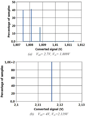
Looking at most of the conversions results for each given pair of values (Vdd, Vin), we observe a dispersion in the results of 1
LSB as shown on the trace of the histograms plotted in Fig.3(a).
(a)! Vdd= 2.7V, Vin= 1.809V
(b)! Vdd= 4V, Vin=2.119V
Fig. 3. Distribution of 100 conversions as a function of Vout performed by the
ADC for different configurations (Vdd, Vin)
As the obtained distributions are neither “predictable” nor “reproducible”, we have isolated some pairs of values (Vdd,
Vin), for which the result of one hundred conversions is only
represented by one bar as for example in the case of Fig. 3(b).
This means that the average is equal to Vin and that the
standard deviation is equal to zero. The best pair of values identified here is: Vdd = 4 V and Vin = 2.119 V.
This pair of values is used to build the conducted immunity behavior model of the AD7476 in static mode against interference signals in the frequency bandwidth from 10 MHz to 1 GHz. At this stage of the study, thanks to [9-10] it is expected that DPI measurements will introduce dispersion into the ADC conversion results. According to previous study, that dispersion in the conversion results, corresponding to a stochastic behavior of the ADC, is due to the random phase of the interference and the stage of the ADC conversion process, driven by the system’s clock.
V.! IMMUNITY BEHAVIORAL MODELLING BY STOCHASTIC
APPROACH
The aim of this part of the study is to determine a mathematical function describing the immunity behavior of the component when an interference signal is injected through the Vdd pin. In order to define this model, several DPI
measurements are performed according to Table 3 and Fig. 2.
First of all, the interference signal is injected through Vdd and
then 100 conversions and acquisitions are performed. This operation is repeated 1624 times (28 frequency values * 58 power values). For each RF disturbance injection, we obtain 100 values. As expected, the DPI measurement introduces dispersions in the conversion results as shown in Fig.4. This is why we choose a stochastic approach to model the behavior of the A/D converter. Hence, for each pair of (Pforw,
freq) we have to identify the statistical distribution that
reproduces as much as possible the samples obtained in measurement.
Fig. 4. Distribution of 100 conversions performed by the ADC during DPI test: Pforw= 26.14 dBm and freq = 1GHz
The most common law identification approach in the literature consists in using the cumulative distribution function (CDF) in addition with the calculation of the KS (Kolmogorov-Smirnov) distance [11]. In the case of our study, the selection Th st id Th be in to ex Table 2: AD7476 tested configurations
Parameters values
Vdd [2.7 V; 5.25 V]; step ≈ 0.25 V
Vin 4== > ?@A=9BCDE
Nbr of conversions 100
1
Rand is function to generate values distributed randomly
FG$2 * 6H >6IC J4,<%4. 45(
5( J > CDD K
LM9
N 45(O DP (4)
Table 3: DPI configuration test
Parameters values Vdd 4 V Vin 2.119 V Pforw [-20 dBm; 35 dBm]; step =1 freq [10 MHz; 1GHz] Nbr of conversions 100
of models (or statistical distribution) is performed thanks to the MAICE (Minimum Akaike Information Criterion Estimate). This last one is widely used in literature and it is considered as an efficient tool for selecting parametric models [11]. The Akaike information criterion (AIC) is defined by the very practical and successful method of MLE (Maximum Likelihood Estimate) and by the number of the model parameters (k). The AIC is calculated by the formula given by Eq. (5).
Thus, the best candidate statistical distribution will be the one that minimizes AIC and has the smallest number of parameters. Note that the number of parameters is useful to make a decision when the MLE is identical for two models. In order to validate the selected model, we use the Kolomogorov-Sminov test. This statistica1 hypothesis test is often used to determine whether a random variable follows a given statistical distribution known for its continuous distribution function. We seek to approximate a sequence of N independent realization of a random variable by a continuous statistical function whose probability density function is fed by empirical characteristic parameters. The list of tested distributions and numbers of their parameters is given in Table 4.
The information criterion described above was used to select the most appropriate distribution (among the twelve statistical distributions listed in Table 4) for each injected disturbance. The statistical distribution selected by MAICE is then validated by the KS test. For this study, the confidence level of KS test is fixed to 10 %. This approach allows us to identify the best distribution that describes the 100 conversions performed by the A/D converter.
Figure 5 is an image composed of 1624 pixels. Each pixel corresponds to one injection disturbance condition (Pforw, freq)
and its color depends on the selected best law. Recall that each statistical distribution is characterized by a finite number of parameters (see Table 4) that are stored in a lookup table and depend on the frequency and the power of the injected signal. The models identified by the information criterion were validated by the Kolmogorov-Smirnov test. To show the adequacy of the selected model and the measurement data we make comparison between the empirical CDF (samples
resulting from measurements) and the theoretical CDF (samples generated by the identified law). As an example, figure 6 proposes the comparison between empirical and 3 different theoretical CDFs for one pixel. Thus, we can validate the selected model for each 1624 studied cases.
Fig. 6. Comparison between the empirical and theoretical CDFs (freq = 60 MHz and Pforw = - 8 dBm)
To simplify the mapping of Fig. 5, we decide to retain only one distribution law for all the 1624 studied cases. So, we plot the number of occurrence of each law on the mapping, the result is presented in Fig.7.
Fig. 7. Number of occurrence of each law
The results show a strong dominance of the normal, the lognormal, and the extreme values distributions. Finally, the selected model is the normal distribution. Its PDF (probability density function) is given by Eq. (6).
GQ! * B.8E > RSTBFU2E V 8 > W6 (5)
Table 4: Tested statistical distributions and their parameters
Continuous statistical distribution Number of
parameters Color code
Weibull 2 Laplace 2 Uniform 2 Exponential 1 Rician 2 Gamma 2 Lognormal 2 Rayleigh 1 Normal 2
Extreme value (EV) 2
Nakagami 2
Generalized extreme value (GEV) 3
Fig. 5. The selected models when RF disturbances are injected through the
Here, µ is the mean and σ is the standard deviation. These two parameters depend on the power and the frequency of the injected disturbance signal and are stored into a lookup table. By using the factor 2.119, corresponding to the particular Vin
previously chosen in section IV, Eq. (6) can be used to model the behavior of the component whatever the Vin value is.
Then, we compare results obtained from DPI measurement techniques to those generated by the model. The immunity criterion is computed using the MAPE (see Eq. (4)) quantifying the errors of conversion in percent. It is fixed to 0.7% (corresponding to an error of 15 LSB). Here, the conversion results (Vout) are generated by the PDF of the
selected model and it is compared to the signal to be converted (Vin). Figure 8 gives the immunity curves between 10 MHz
and 1 GHz plotted by using different laws.
Fig. 8. Comparison between measurement and models
The results confirm that the normal law allows modelling the immunity behavior with a good agreement.
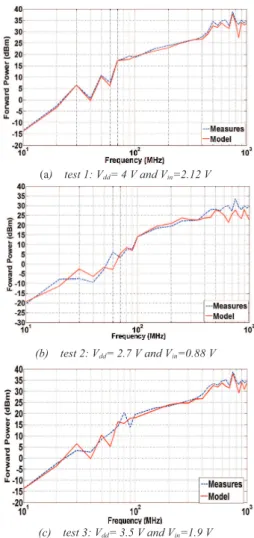
Finally, the purpose is to demonstrate that the model works for different values of Vin. Note that the choice of the polarized
voltage Vdd has no impact on the conversion results when it
takes value between 2.7 V and 4 V. As shown in Table 5, the DPI curves are computed and measured in three configurations of the ADC.
Figures 9(a), 9(b) and 9(c) (test1, test2 and test3, respectively) give the immunity curves between 10 MHz and 1 GHz plotted using the normal law.
(a) test 1: Vdd= 4 V and Vin=2.12 V
(b) test 2: Vdd= 2.7 V and Vin=0.88 V
(c) test 3: Vdd= 3.5 V and Vin=1.9 V
Fig.9. Comparison between measurements and model
We observe for all considered cases that the immunity curves increase with the frequency. The immunity curves derived from measurements and the model give good results.
VI.! CONCLUSION
In this paper, we presented a new modeling approach for the construction of an immunity behavioral model for the AD7476 from Analog Devices. Thanks to the information criterion, the behavior of the A/D converter against the RF disturbances was modeled by statistical distributions whose parameters depend on the power and the frequency of the injected signal. The immunity criterion used here made it possible to identify the level of power required to induce an average percentage of the errors of conversion. The simulated immunity curves are in a good agreement with those obtained through DPI measurements.
ACKNOWLEDGMENT
This work is supported by the IRT Saint-Exupery’s Electronics Robustness project sponsored by Airbus Operations, Airbus Group Innovations, Continental Automotive France, Hirex Engineering, Nexio, Safran Electrical & Power, Thales Alenia Space France, Thales XBYZ 6[N \E * 6 C \BX?]^N $5(_E`8a > bcd6B.6BY . B [eX?]^N $5(_f 8PCCg > 45(EE: 8\BX?]^N $5(_E: E (6)
Table 5: Tested configurations
Test number Vdd (V) Vin (V)
test 1 4 2.12
test 2 2.7 0.88
Avionics and the French National Agency for Research (ANR).
REFERENCES
[1] S. R and al, "Electronic part life cycle concepts and obsolescence forecasting," IEEE Transactions on Components
and Packaging Technologies, 2000.
[2] A. Durier and al, "A methodologic project to characterize and model COTS components EMC behavior after ageing,"
APEMC proceeding 7th Asia Pacific International Symposium, 2016.
[3] H. Huang and al, "Prediction of Aging Impact on Electromagnetic Susceptibility of an Operational Amplifier,"
Asia-Pacific International EMC Symposium, 2015.
[4] R. Fernandez-Garcia and al, "Impact of Temperature on the Electromagnetic Susceptibility of Operational Amplifiers,"
Progress in Electromagnetics Research Symposium, 2012.
[5] T. Dubois and al, "Characterization and model of temperature effect on the conducted immunity of Op. Amp,"
Microelectronics Reliability, 2015.
[6] S. Hairoud and al, "Multiport ICIM-CI modeling approach applied to a bandgap voltage reference," EMC
Europe 2016, 2016.
[7] Y. Kondo and al, “Simulation of Bulk Current Injection Test Using Integrated Circuit Immunity Macro Model and Electromagnetic Analysis”, EMC Europe 2016, 2016.
[8] S. Op ’T Land and al, “Immunity Modeling of the LM2902 Operational Amplifier”, EMC Europe 2010, 2010. [9] J-B. Gros and al, "VHDL-AMS relevance for predicting integrated circuits emissivity and immunity," EMC Europe
2011, 2011.
[10] A. Ayed and al, "Immunity Measurement and Modeling of an ADC Embedded in a Microcontroller Using RFIP Technique," IEEE Transactions on Electromagnetic Compatibility, 2015.
[11] RM. Secareanu and al, "Physical design to improve the noise immunity of digital circuits in a mixed-signal smart-power system," IEEE International Symposium on Circuits