Pépite | Réalisation et caractérisation de transistors à effet de champ organiques OFETs et Mémoires à nano grille flottante sur des substrats rigides et flexibles
148
0
0
Texte intégral
(2) Thèse de Shuo Li, Université de Lille, 2018. © 2018 Tous droits réservés.. lilliad.univ-lille.fr.
(3) Thèse de Shuo Li, Université de Lille, 2018. Acknowledgements First and foremost, I would like to express my deep and sincere appreciation to my supervisor Prof. Kamal Lmimouni for continuous support of my Ph. D study and research, I am grateful for his patience, kindness, expertise and excellence guidance. I still remember the first day that he introduced me to the group members and showed me the instruments in our Laboratory, which encouraged me to start and insist my research work in IEMN. With his supervision and constant help, it has been possible for me to achieve this doctoral thesis. I am grateful to Prof. Bernard Ratier and Prof. Laurence Vignau for their great contribution to review this thesis. I also wish to thank Prof. Tuami Lasri, Prof. Christian Legrand and A. Prof. Marc Ternisien for participating to the jury in my defense and examining my research work. My sincere thanks to my NCM group members and my dear friends in the same office. Dr. David Guérin, Dr. Bilel Hafsi, Dr. Sébastien Pecqueur, Dr. Tianchen Zhang, Dr. Stéphane Lenfant, who gave me a lot of assistance for device fabrication in cleanroom and introduced me the characterization in our department. Mr. Louis Thomas helped me do the AFM measurements. Also, I am grateful for Dr. Dominique Vuillaume, Dr. Fabien Alibart, Ms. Khaoula Ferchichi et. al., their friendly help and suggestions during my work made me feel I was in a big warm unity with great friendship. During the last three years, as I worked a lot in the cleanroom for device fabrication and characterization, I would also like to express my gratitude to all the IEMN cleanroom staffs for their constant technical support. Many thanks to Mrs. Annie Fattorini and Mr. Marc Dewiit for metal deposition, Mr. François Vaurette and Mr. Pascal Tilmant for the lithography technique, and Mr. Jean-Louis Codron for his help in XPS measurement. Thank Ms. Nora Benbahlouli, Ms. Malika Habbas, Ms. Emmanuelle Gillmann for helping me deal with many things. Besides, I have also to thank all my friends: Natalia, Jianping Hao, Di Zhou, Wei Wei, Tianjun Lin, Tianqi Zhu, Sijia Gu, Xiaoping Hou, Haifeng Yuan, Stanislav, Sarah, Abderrahmane et.al. for their help, emotional support and entertainment in the last three years. Last but not the least, I would like to express my appreciation to my family members, who always give me endless love, encouragement and spiritual support throughout my life.. © 2018 Tous droits réservés.. lilliad.univ-lille.fr.
(4) Thèse de Shuo Li, Université de Lille, 2018. © 2018 Tous droits réservés.. lilliad.univ-lille.fr.
(5) Thèse de Shuo Li, Université de Lille, 2018. Table of content. Table of content Table of content .................................................................................................................... I List of abbreviations ........................................................................................................... V List of samples.................................................................................................................. VII. General introduction ........................................................................................................... 1 Chapter 1 State of the art ................................................................................................... 3 1.1 Background .................................................................................................................. 3 1.2 Overview of organic field-effect transistor (OFET) .................................................... 5 1.2.1 Synthesis of organic semiconductors ................................................................ 5 1.2.2 Structures and operations of OFET ................................................................... 6 1.2.3 Extraction of electrical parameters .................................................................... 8 1.2.4 High mobility p-type organic semiconductors ................................................ 11 1.2.5 Pentacene based OFET.................................................................................... 14 1.3 Overview of OFET based nano-floating gate memory .............................................. 21 1.3.1 Structure and operations .................................................................................. 21 1.3.2 Nano-floating gate layers ................................................................................ 22 1.3.3 Pentacene based NFGM .................................................................................. 24 1.4 Conclusions ................................................................................................................ 27 References ........................................................................................................................ 28. Chapter 2 Preparation and optimization of organic transistors ................................... 37 2.1 Introduction ................................................................................................................ 37 2.2 Fabrication of pentacene based OFETs ...................................................................... 38 2.2.1 Electron-Beam Lithography technology ......................................................... 38 2.2.2 Self-assembled monolayer (SAM) modification............................................. 42 I © 2018 Tous droits réservés.. lilliad.univ-lille.fr.
(6) Thèse de Shuo Li, Université de Lille, 2018. Table of content 2.2.3 Thermal evaporation ....................................................................................... 43 2.3 Instrumentations ......................................................................................................... 44 2.3.1 Contact angle measurements ........................................................................... 45 2.3.2 Atomic force microscopy ................................................................................ 46 2.3.4 XPS and UPS .................................................................................................. 47 2.3.5 Electrical characteristic system ....................................................................... 48 2.4 Characterization ......................................................................................................... 48 2.4.1 Physical properties .......................................................................................... 48 2.4.2 Electrical properties......................................................................................... 51 2.4.3 Analysis of physical mechanisms ................................................................... 56 2.5 Conclusions ................................................................................................................ 61 References ........................................................................................................................ 62. Chapter 3 Preparation and characterization of NFGM ................................................ 66 3.1 Introduction ................................................................................................................ 66 3.3 The memory electrical properties ............................................................................... 73 3.3.1 The memory performances of SAM modified DFG memory ......................... 73 3.3.2 The effects of rGO sheets ................................................................................ 77 3.3.3 The effects of PFBT SAM .............................................................................. 82 3.4 The comparison of electrical parameters ................................................................... 86 3.5 Conclusions ................................................................................................................ 87 References ........................................................................................................................ 89. Chapter 4 Preparation and characterization of OFET and NFGM on flexible substrate ............................................................................................................................. 93 4.1 Introduction ................................................................................................................ 93. II © 2018 Tous droits réservés.. lilliad.univ-lille.fr.
(7) Thèse de Shuo Li, Université de Lille, 2018. Table of content 4.2 Experimental .............................................................................................................. 94 4.2.1 Fabrication of flexible OFET .......................................................................... 94 4.2.2 Fabrication of flexible NFGM....................................................................... 100 4.3 Characterization of pentacene based OFET ............................................................. 105 4.3.1 Electrical characteristics ................................................................................ 105 4.3.2 Extractions of electrical parameters .............................................................. 115 4.4 Characterization of pentacene flexible NFGM ........................................................ 116 4.4.1 The memory electrical properties .................................................................. 116 4.4.2 The analysis of mechanisms .......................................................................... 124 4.5 Conclusions .............................................................................................................. 125 References ...................................................................................................................... 126 Conclusions and perspective ........................................................................................... 129 List of publications .......................................................................................................... 131. III © 2018 Tous droits réservés.. lilliad.univ-lille.fr.
(8) Thèse de Shuo Li, Université de Lille, 2018. IV © 2018 Tous droits réservés.. lilliad.univ-lille.fr.
(9) Thèse de Shuo Li, Université de Lille, 2018. List of abbreviations. List of abbreviations OFET. Organic Field Effect Transistor. OSCs. Organic Semiconductors. NVM. Nonvolatile Memory. NFGM. Nano-floating Gate Memory. MIS. Metal-Insulator-Semiconductor. HOMO. Highest Occupied Molecular Orbital. LUMO. Lowest Unoccupied Molecular Orbital. S/D. Source/Drain. SAM. Self-assembled Monolayer. PMMA. Polymethylmethacrylate. Au NPs. Gold Nanopaticles. NCs. Nanocrystals. OTS. 3-Octadecyltrichlorosilane. rGO. Reduced Graphene Oxide. PFBT. 2,3,4,5,6-Pentafluorobenzenethiol. EBL. Electron-Beam Lithography. AFM. Atomic Force Microscopy. SEM. Scanning Electron Microscopy. XPS. X-ray Photoelectron Spectroscopy. UPS. UV-Photoelectron Spectroscopy. RMS. Root Mean Square Roughness. W/L. Channel Width /Channel Length. DFG. Double Nano-floating Gate. SFG. Single Nano-floating Gate V. © 2018 Tous droits réservés.. lilliad.univ-lille.fr.
(10) Thèse de Shuo Li, Université de Lille, 2018. List of abbreviations APTS. 3-Aminopropyl)triethoxysilane. P/E. Program/Erase. PC. Parylene C. PVD. Physical Vapor Deposition. CVD. Chemical Vapor Deposition. HSQ. Hydrogen Silsesquioxane. UV-zone. Ultraviolet-Ozone. Ref.. References. VI © 2018 Tous droits réservés.. lilliad.univ-lille.fr.
(11) Thèse de Shuo Li, Université de Lille, 2018. List of samples. List of samples Rtot. Total resistance (Ω). RC. Contact resistance (Ω). Rch. Resistance of channel (Ω). L. Channel length (µm). W. Channel width (µm). μ. Charge carrier mobility (cm2V-1s-1). Ci. Gate capacitance per unit area (F/cm2). VGS. Gate-source voltage (V). VDS. Source-drain voltage (V). IDS. Source-drain voltage (A). Ion/Ioff. Current on–off ratio. θ. Contact angle (°). VTh. Threshold voltage (V). ∆VTh. Memory window (V). S. Subthreshold swing (V/decade). max 𝑁ss. Maximum number of interface states (cm-2 eV-1). k. Boltzmann constant. T. Absolute temperature (°). q. Electronic charge (C). Δn. Number of trapped charges in the Au NPs (and polymer electret). VII © 2018 Tous droits réservés.. lilliad.univ-lille.fr.
(12) Thèse de Shuo Li, Université de Lille, 2018. VIII © 2018 Tous droits réservés.. lilliad.univ-lille.fr.
(13) Thèse de Shuo Li, Université de Lille, 2018. General introduction. General introduction In the various of electrical devices, organic field effect transistor (OFET) have been attracted great attention over the past few years because of a number of merits such as low-cost process, potential to realize large areas, and particularly that they are compatible with flexible plastic circuits. Nowadays, the OFET based nonvolatile memory (NVM) devices. i. e. flash memory, which means the information could be remain stored even when power is disabled, is also one of the most important and fundamental elements in the construction of electronic systems. Generally, the flash memory could be classified in terms of the structures and materials of the charge storage layers, among the many possible device configurations of organic flash memories, tremendous efforts have been devoted to the development of nano-floating gatebased transistor memories (NFGM) towards high performance memory devices (exhibit high speed operation, superior reliability, and to be scaled down), due to its spatially discrete floating-gate elements (nanometer-sized metallic or semiconductor nanoparticles) effectively as a charge trapping site between two dielectric layers (blocking layer and tunneling layer. Considering the effects of materials and process conditions, the characteristics of the pentacene based NFGM were improved more or less that have been reported. The objective of this work is to develop pentacene based OFET and NFGM devices on flexible substrates. There are mainly three parts involved; (i) Optimization of the OFET that fabricated on conventional Si/SiO2 substrate; (ii) Improvement of the performances of NFGM based on the results of OFET;(iii) Realization of OFET and NFGM on flexible substrate. In chapter 1, first, the introduction of the OFET and NFGM is described. Then, the typical high mobility p-type organic semiconductors that are widely used in OFET devices are demonstrated. Based on the widely literatures and the mature fabrication process in our group, the pentacene is chosen as the organic semiconductors in this thesis, thus, the progress of pentacene based OFET and NFGM devices that reported in recent years has been introduced. According to the reports, the self-assembled monolayer (SAM) is presented to optimize the OFET. To fabricate the NFGM, Au nanoparticles (Au NPs) and reduced graphene oxide (rGO) sheets are chosen as the floating gate layers in this work. In chapter 2, the fabrication processes of our OFET samples on rigid substrates and the analysis instrumentations are described in detail. The physical and electrical properties of different SAM modified pentacene FET devices were performed and discussed, i.e. pentacene 1 © 2018 Tous droits réservés.. lilliad.univ-lille.fr.
(14) Thèse de Shuo Li, Université de Lille, 2018. General introduction deposited on OTS modified dielectric surfaces, on the PFBT modified source/drain electrodes, and on the cumulative OTS and PFBT modified surfaces. The FET of pentacene deposited on bare SiO2 was fabricated as a reference. Then, the electrical parameters of the different samples of OFET were summarized and compared. Through the SAM modification, optimized electrical performances were obtained and the charge transport mechanisms were explained. In chapter 3, the pentacene based single floating gate (SFG) memory (using Au NPs as trap layer) and double floating gate (DFG) memory (using Au NPs and rGO as the lower and upper trap layer, respectively) were fabricated and characterized. The SiO2 and Al2O3 dielectrics were deposited as blocking layer and tunneling layer, respectively. Based on the results of chapter 2, the PFBT was used to modify our memory devices, the performances our NFGM devices with and without PFBT modification were demonstrated and compared. Meanwhile, the effects of rGO sheets and the effects of SAM modification on the NFGM were discussed. Finally, Optimized memory performances including the large memory window of 51 V, the stable retention property more than 108 s, and reliable cycling endurance over 1000 cycles were obtained. This further highlights the utility of surface modulations to tune the charge storage/release behaviors in transistor memories. In chapter 4, first, the performances of pentacene based transistors that fabricated on flexible substrates were presented. The materials used in this transistor are all organics and the fabrication processes are under low temperatures. The operation voltage of the flexible OEFT was deduced compared to the one that fabricated on Si substrate and there was no hysteresis in the I-V measurements, which means the interface traps were well decreased. Then, the NFGM devices were fabricated on flexible substrates and the performances were demonstrated. In particular, the multi-level data storage was achieved from our flexible NFGM, from the bending stability/mechanical stability test, the stable retention property more than 105 s, and reliable cycling endurance over 500 cycles were obtained. In chapter 5, the conclusions of this thesis are summarized and discussed, based on the results of this thesis, the perspective is proposed.. 2 © 2018 Tous droits réservés.. lilliad.univ-lille.fr.
(15) Thèse de Shuo Li, Université de Lille, 2018. Chapter 1 State of the art. Chapter 1 State of the art. 1 © 2018 Tous droits réservés.. lilliad.univ-lille.fr.
(16) Thèse de Shuo Li, Université de Lille, 2018. Chapter 1 State of the art. 2 © 2018 Tous droits réservés.. lilliad.univ-lille.fr.
(17) Thèse de Shuo Li, Université de Lille, 2018. Chapter 1 State of the art. Chapter 1 State of the art 1.1 Background Current research on electronic devices have been advancing incredibly fast as much of our life relies on them, the miniaturization and economically applicable are all along great demand for the realization of industrial production. In the various electronic devices, organic field effect transistor (OFET) has been attracted great attention over the past few years because of a number of merits such as low-cost process, potential to realize large areas, and particularly that they are compatible with flexible plastic circuits [1-5]. In the improvement of material performances, since the organic materials used for the OFET fabrication such as the semiconductors, the dielectrics and even the substrates could be deposited at room temperature or relatively at low temperatures. In addition, most of the organic materials are available for deposition in solution, thus the deposition process could be adopted as spin-coating or inkjetprinting that avoid to require a vacuum stage. Otherwise, in the past of years, many organic semiconductors (OSC) have been found high field-effect mobilities (up to 10 cm2V-1s-1 or even higher) that exceed the mobilities (0.5–1.0 cm2V-1s-1) of amorphous silicon, for instance, pentacene, rubrene, and fullerene (C60), the typical OSC used in OFET [6, 7]. As the output current and cut-off frequency are proportional to the mobility, it is essential to obtain high mobility for device applications. The progress of OSC in mobility and the economy of the fabrication process make OFET has great potential in various real electrical applications based on the industrial manufacturing technology. As a result, for the applications of OFET, they have been expected and proposed to be used as display switches [8], chemical and biological sensors [9, 10], liquid crystals [11], neuromorphic synapses [12, 13], nonvolatile memories [14-16] and so on. In terms of the OFET memory devices, they have the similar geometry as OFET, the difference is that a charge-storing medium like a thin film, or metallic/semiconductive discrete NPs act as floating gate between two dielectric layers for the OFET memory devices [17, 18]. Nowadays, the nonvolatile memory (NVM), which means that the information could be remain stored even when power is disabled, is also one of the most important and fundamental elements in the construction of electronic systems [19-21]. As a conventional NVM, Si-flash memory has been extensively used in mobile storage for a long period of years due to their 3 © 2018 Tous droits réservés.. lilliad.univ-lille.fr.
(18) Thèse de Shuo Li, Université de Lille, 2018. Chapter 1 State of the art massive memory capacity, relatively high density and low fabrication process [22]. Generally, the flash memory could be classified in terms of the structures and materials of the charge storage layers, including conventional floating gate type memory by using a conducting floating gate, nitride-based charge trapping memory [23] and NPs or nanocrystals (NCs) based charge trapping memory (called nano-floating gate memory NFGM) [24], they have the common configuration that the trapping layer assembled between two dielectric layers, which called tunneling layer and blocking layer, respectively. Figure 1.1 shows the device structure of a conventional flash memory cell.. Figure 1.1 Device structure of a conventional flash memory cell.. As portable electronic devices scaling continues, and requirements such as high performance, high density, low power consumption for NVM devices, a lot of challenges have been met for us to optimize the conventional floating gate type flash memory. For example, it is very difficult to reduce the tunneling layer because of the charge loss and stress-induced leakage current [25], and the reduction of the dimensions of the floating gate will decrease the stored electrons/holes, which makes the margin of the electron/hole loss tolerance very narrow [26]. Thus, considering these drawbacks, the emerging flash memory of NFGM type has been proposed and studied. One hand, the NPs (NCs) are discretely assembled between the tunneling layer and the blocking layer that avoid the problem of using a continuous floating gate, on the other hand, the reap levels and trap sites could be effectively controlled and tuned by the work functions and dimensions (size and density) of the NPs [28]. Hence, a tremendous efforts has been devoted to develop NFGM devices in recent decades, it has been considered as a promising 4 © 2018 Tous droits réservés.. lilliad.univ-lille.fr.
(19) Thèse de Shuo Li, Université de Lille, 2018. Chapter 1 State of the art candidate towards high performance flash memory devices that shows large endurance, small size, long retention time, and low power consumption [29, 30]. Among the many possibility applications of NFGM, by using OSC to enable the NFGM, it gives a great opportunity to fulfill the requirements for novel applications targets such as flexible, printable, and low-cost preparation processes [31].. 1.2 Overview of organic field-effect transistor (OFET) 1.2.1 Synthesis of organic semiconductors Organic transistors are metal-insulator-semiconductor (MIS) field-effect transistors (FETs) in which the semiconductor is a conjugated organic material [32]. Generally, the conjugated bands including the sigma (σ)-type bond a pi (π)-type bond, σ-bonds are the strongest in covalent bonds and π-bonds are much weaker than them. In σ-bonds, both bonded atoms give single electron from the s orbital and the two electrons are attached to their nuclei and localized. In π-bonds, the two electrons come from the p orbitals which are far away from their nuclei, and the two electrons are localized as well. Organic semiconductors are conjugated polymers which consist of sp2–hybridized linear carbon chains. These chains hold a sp2-2pz configuration in double bond, overlapping among different sp2 orbitals forms σ bonds. On the other hand, two pz orbitals form a less strong covalent bonds called π bonds as shown in figure.1.2 [33].. Figure 1.2 Sp2 hybridization of two carbon atoms. Sp2 orbitals lie on the same plane and bond into an σ-bond, pz orbitals are orthogonal to the plane and bond into a π-bond.. 5 © 2018 Tous droits réservés.. lilliad.univ-lille.fr.
(20) Thèse de Shuo Li, Université de Lille, 2018. Chapter 1 State of the art For the band diagram of OSCs, as alternating double and single bonds in the conjugated backbone results in a separation of bonding and anti-bonding states, causing the formation of a forbidden energy gap and a spatially delocalized band-like electronic structure. The highest occupied molecular orbital (HOMO) consists of bonding states of the π -orbitals with filled electrons, and is analogous to the valence band in silicon. The lowest unoccupied molecular orbital (LUMO) consists of empty higher energy anti-bonding (π∗) orbitals, and is analogous to the conduction band. The energy difference between the HOMO and LUMO defines the band-gap energy (Eg), as shown in figure 1.3. Eg depends on the chemical structure of the repeating unit, and generally decreases with the number of repeat units in the chain [33]. The Eg of conjugated polymers is typically in the energy range of 1–4 eV. This band-like structure, along with low electronic mobility, is responsible for the semiconducting properties observed in conjugated polymers.. Figure 1.3 Energy band diagram of an organic semiconductor. Abbreviations: IP: ionization potential; LUMO: lowest unoccupied molecular orbital; HOMO: highest occupied molecular orbital.. 1.2.2 Structures and operations of OFET • Structures Generally, the common configurations used for FETs are devised into two different structures, i. e. bottom-gate type and top-gate type, as shown in figure 1.4 [34]. The structure of the device contains the layers of substrate (rigid or flexible), gate electrode, insulator (dielectric), semiconductor, and source and drain electrodes. In addition, because of the different positions of source and drain electrodes, the structures of FET could be identified detail as bottom-gate-bottom-contact (BGBC), bottom-gate-top-contact (BGTC), top-gate6 © 2018 Tous droits réservés.. lilliad.univ-lille.fr.
(21) Thèse de Shuo Li, Université de Lille, 2018. Chapter 1 State of the art bottom-contact (TGBC), as well as top-gate-top-contact (TGTC). Briefly, each structure has the merits and drawbacks, the choice of the structure is normally decided by the fabrication processes such as the temperatures, the circumstance conditions, the lithographic masks involved and the materials (metals, dielectrics and semiconductors) that used for the realization of device. In the case of OFETs, the semiconductor is an organic material. The OSCs are the most important materials that are used as the active components for OFET, they can be divided into n-type with electrons transporting and p-type with holes transporting, as well as ambipolar ones with both electrons and holes transporting.. Figure 1.4 Typical device structures of organic field-effect transistors.. • Operations In principle, the electrical characteristic that best to be used to define the OFET is the presence of the electric field that controls and modulates the conductivity of the channel between source and drain electrodes, i. e. the current between source and drain (IDS) [34]. The typical p-type and n-type OFET operations (BGTC structure) are shown in figure 1.5 (a) and (b). The electric field is created by the gate voltage between gate and source (V GS), which is also dependent on the insulator (dielectric) layer. For the different type of semiconductor, a positive or a negative gate voltage will be operated to force the holes or electrons (charges) accumulate at the insulator (dielectric) and semiconductor interfaces. And the density of the 7 © 2018 Tous droits réservés.. lilliad.univ-lille.fr.
(22) Thèse de Shuo Li, Université de Lille, 2018. Chapter 1 State of the art charges is dependent on the VGS and capacitance (C) of the insulator. Figure 1.5 (c) and (d) show the energy-level diagrams along the carriers transport in the channel of p-type and n-type organic transistors, respectively. In p-channel transistors the transfer of negative charges into the semiconductor is blocked due to the large energy difference between the Fermi level of the contact and the LUMO of the semiconductor, and in n-channel transistors the transfer of positive charges is blocked by the energy barrier between the contact and the HOMO of the semiconductor [32].. Figure 1.5 Typical operations of (a) p-type and (b) n-type organic field-effect transistors. L, channel length; W, channel width. Energy-level diagrams along the carriers transport in the channel of organic transistors: (c) p-channel transistor, (d) n-channel transistor. Abbreviations: WF: work function; EA: electron affinity; IP: ionization potential; LUMO: lowest unoccupied molecular orbital; HOMO: highest occupied molecular orbital; EF: Fermi energy level.. 1.2.3 Extraction of electrical parameters The electrical parameters for the OFET are commonly extracted from the typical current-voltage characteristics, which involves static current versus voltage measurements, where output (IDS-VDS, VDS is the voltage between source and drain) and transfer (IDS-VGS). 8 © 2018 Tous droits réservés.. lilliad.univ-lille.fr.
(23) Thèse de Shuo Li, Université de Lille, 2018. Chapter 1 State of the art curves can be obtained. As shown in figure 1.6, an example of an n-type device with typical “near”-ideal output and transfer I-V curves.. Figure 1.6 Typical (a) output and (b) transfer characteristics of an n-type OFET.. For the output curves that shown in figure 1.6 (a), the characteristic provides a most qualitative information of the effectiveness of channel pinch-off and contact resistance between electrodes and probes of the equipment. As OFET is being seriously assessed for mobility critical applications, it is very important to extract the value of the mobility [6]. As we can see in figure 1.6 (b), when VGS>VTh, a significant density of charges is accumulated in dielectric/semiconductor interface and a large. IDS. starts flowing, depending on the VDS. This. state is designated by On-state and involves a linear current regime at a low VDS and followed by a saturation regime at a higher VDS value, for the two regimes, the IDS varies with the VGS are determined as following: When VDS˂<VGS-VTh, the OFET is in the linear mode, the IDS is ascribed: I D S Ci lin ear . W 1 (VG S VTh )VD S VD2S L 2 . (1-1). where Ci is the gate capacitance per unit area, µliner the field-effect mobility, W is the channel width, and L the channel length of the device. For VDS˂VGS-VTh, the quadratic term is typically neglected. When VDS˃˃VGS- VTh, the OFET is in the saturation mode, the IDS is ascribed: I DS (. W ) Ci sat (VGS VTh ) 2 2L. (1-2). where µsat the field-effect mobility. 9 © 2018 Tous droits réservés.. lilliad.univ-lille.fr.
(24) Thèse de Shuo Li, Université de Lille, 2018. Chapter 1 State of the art Based on the equation of (1-2), the µsat which is extremely relevant to evaluate the performance of OFET is obtained and describes a situation when the channel width W is smaller than length L [35].. sat. d I DS 2 L dVGS CiW. . 2. (1-3). In general, these electrical parameters not only depend on the nature properties of the materials, but also on the structure of the OFET, and on fabrication technologies that may induce traps. In addition, using the equation (1-3), conservative mobility estimates are preferable even considering some of the high mobility materials exhibit non-idealities in their transfer and output characteristics, but many of the reported high-mobility materials exhibit near ideal transfer characteristics [6, 36, 37]. And from the transfer curves, more electrical analysis are discussed and the relative electrical parameters are defined, the details of the other basic parameters are determined as below: • Contact resistance (Rtot): This parameter is opposed to an intrinsic value in a transistor system refers to the contribution on the total resistance of the channel length (Rch) and the electrodes connections (Rc). Consequently, a small contact resistance is preferable. • Current on–off ratio (Ion/Ioff): The parameter is a ratio value of the maximum IDS to minimum IDS. It is known that a higher “on” current offers better driving capability, while a lower “off” current results in low leakage current [38]. Consequently, a higher Ion/Ioff ratio value is preferable. • Threshold voltage (VTh): It is a significate parameter that reflects a significant charge is accumulated close to the dielectric/semiconductor interface, which corresponds to the VGS. By using a linear extrapolation of the IDS-VGS at low VDS, the VTh could be obtained. • Turn-on voltage (Von): This parameter corresponds to the VGS at which IDS starts to rapidly increase. It is easily visible in the log IDS-VGS curves. • Subthreshold swing (S): this parameter indicates the VGS required to increase IDS by one decade, as seen in the subthreshold region. It is defined in V/decade: d log I DS S dVGS . 1. (1-4). 10 © 2018 Tous droits réservés.. lilliad.univ-lille.fr.
(25) Thèse de Shuo Li, Université de Lille, 2018. Chapter 1 State of the art Normally, a small threshold swing indicates lower power consumption and higher switch speed for the transistor device [38]. With these basic electrical parameters, we can analyze the qualitative performances of the OFET device. For instance, considering the operation of n-type OFET, the positive and negative value of VTh could design the device as enhancement and depletion mode, respectively. The enhancement mode is typically preferable as a gate voltage is not necessary to turn off the device [39].. 1.2.4 High mobility p-type organic semiconductors One of the most important step is to choose an OSC material as the active component. The OSC is the OFET device core element because semiconductor controls charge transport in the FET. That’s because the device mobility, which is the key parameter for an OTFT, is an indicator of charge transport efficiency through the semiconductor channel. In the past of years, the organic semiconductor materials that have been most used include both sublimed and solution processed semiconductors such as pentacene, tips-pentacene, fullerene, rubrene. The choice of the semiconductor materials highlight several possibilities to develop integrated circuit technologies based on OFET for various large area, low-cost applications. Generally, Organic semiconductors are generally classified into polymers and small molecules. Polymers have lower performance than small molecules, however, polymers are more susceptible and flexible to various deposition techniques. Oxidation and reduction reactions are used to achieve p-type (electron removal) and n-type (electron addition) doping, respectively. Usually, polymers are doped by oxidation, that’s why p-type conductive polymers are more common. Here, some of the typical p-type OSCs are presented as below:. • P-type small molecular In the variety of p-type OSCs, pentacene is one of the well-known p-type small molecular and the promising semiconductors with high mobility that has been widely and intensively used in many years. For example, the OFET built on purified pentacene by using parylene gate dielectric obtained the mobility of 2.2 cm2V-1s-1 [40]. A mobility of 1.4 cm2V-1s1. was found for the pentacene single crystals by using a SiO2 gate dielectric that treated with. self-assembled monolayer (SAM) [41]. Very recently, a carrier mobility of 4.63 cm2V-1s-1 for the pentacene OFET with La0.850Nb0.150Oy as gate dielectric has been reported [42]. And for the pentacene fabricated with flexible substrate, P. Cosseddu et al [43] found the mobility of 11 © 2018 Tous droits réservés.. lilliad.univ-lille.fr.
(26) Thèse de Shuo Li, Université de Lille, 2018. Chapter 1 State of the art (5±2)×10-2 cm2V-1s-1 for the pentacene fabricated on poly(ethylene therephtalate) (PET) substrate and using the parylene as dielectric layer. Kwang H. Lee [44] et al reported a higher mobility of 1.22 cm2V-1s-1 for pentacene based OFET deposited on polyethersulfone (PES) substrate. Furthermore, the OFET based on a bulk and ultrapure single crystal of pentacene was reported to exhibit very high hole mobilities values in the range of 15∼40 cm2V-1s-1 at room temperature by using 6,13-pentacenequinone (PQ) as the gate dielectric [45]. Otherwise, rubrene is another p-type small molecular that used extensively in OFET devices, it also has exhibited the optimized charge carrier mobilities as high as ∼15 cm2V-1s-1 by a fabrication method of laminating a monolithic elastomeric transistor stamp against the surface of a crystal [46] and the mobility is even maximized to ∼43 cm2V-1s-1 [47]. In addition, a functionalized small molecule pentacene, 6,13-bis-(triisopropylsilylethynyl) (TIPS-pentacene) has been researched widely because of their relatively high field-effect mobility and soluble in many common solvent with solution process ability. The mobility of TIPS-pentacene has been reported as 4.6 cm2V-1s-1 with the shortest π-π stacking distance of 3.04 Å achieved by lattice strain that prepared by a solution-shared technique [48]. And Zhenan Bao et al showed the mobility of Tips-pentacene up to 2.7 cm2V-1s-1 that designed OFET with very small pattern [49]. Jae-Joon Kim et al reported highly crystalline and selfassembled TIPS-Pentacene with maximum mobility of 3.40 cm2V-1s-1 that formed by simple spin-coating [50]. TIPS-pentacene also deposited on flexible PEN substrate and showed a promising performance with a mobility of 0.8 cm2V-1s-1 [51]. Totally, the mobility of TIPSpentacene based OFET was improved up to 11 cm2V-1s-1 through a “fluid-enhanced crystal engineering” device fabrication approach [52]. In recent years, a small molecule 2,7-dioctyl[1]benzothieno[3,2-b][1]-benzothiophene (C8-BTBT) has attracted much attention since it is ultra-transparency, and with high mobility. A maximum hole mobility values of 31.3 cm2V-1s-1 for C8-BTBT was obtained by printing method [53]. And it even showed mobility values as high as 43 cm2V-1s-1 by using a blended solution with polystyrene [54]. Very recently, the hole mobility of C8-BTBT at room temperature reaches 6.50 cm2V-1s-1 by easy treatment way with UV-ozone exposure on the SiO2 surface [55].. • P-type polymer semiconductors For the OFET fabricated with polymers OSCs, a large effort and several strategies have been developed these years, and several materials with home mobility over 1 cm2V-1s-1 have 12 © 2018 Tous droits réservés.. lilliad.univ-lille.fr.
(27) Thèse de Shuo Li, Université de Lille, 2018. Chapter 1 State of the art been reported [56]. Basically, poly-(3-hexylthiophene) (P3HT) is the benchmark p-type polymeric. OSCs. for. dialkylquaterthiophenes). OFET (PQT). with. mobility. [58],. of. 0.1. cm2V-1s-1 [57].. Poly-(3,3-. poly(2,5-bis(3-alkylthiophen-2-yl)thieno[3,2-b]. thiophene) (PBTTT) [59] were introducing functionalized groups into the main chain of polythiophenes, improving the mobility up to cm2V-1s-1. The mobility of co-polymers reported in reference (Ref.) [60] with donor-donor type structure by integrating the advantages of PQT and PBTTT was 4.6 cm2V-1s-1, respectively. However, among the many types of polymers, donor-acceptor type co-polymers dominate the highest mobility in OFET application. Copolymers based on fused PBTTT derivatives are interesting polymers with mobility up to 10 cm2V-1s-1 [56, 61]. Further improvement of long-range orientation of the polymer chains based donor-acceptor co-polymers obtained much improved mobility, the mobility reached up to 23.7 cm2V-1s-1 in Ref. [62] and 21.3 cm2V-1s-1 in Ref. [63]. Figure 1.7 shows the molecular structures of some typical P-type organic semiconductors with high mobility (a) small molecules (b) polymers.. Figure 1.7 Molecular Structures of some typical P-type organic semiconductors with high mobility (a) small molecules, (b) polymers.. 13 © 2018 Tous droits réservés.. lilliad.univ-lille.fr.
(28) Thèse de Shuo Li, Université de Lille, 2018. Chapter 1 State of the art In this part, several p-type representative OSCs are mentioned, much more high mobility of OSCs were reported in detail in the review references of [64]. As using the n-type OSCs in OFET devices, the electrons should be injected into LUMO level of the semiconductor, and most of the values of energy diagrams at the LUMO level are around 4.0 eV, thus, it needs relatively low work function electrodes for better charge injection. However, the electrodes with low work function is not as stable as gold (Au), platinum (Pt) electrodes with high work function in the air, thus we considered to use typical p-type semiconductor. Moreover, pentacene, which is an aromatic hydrocarbon and is shown in figure 1.7, is one of the promising materials with high mobility and has been widely and intensively studied that more than 1000 articles related to pentacene transistors have been reported in scientific journals confirming its considerable importance. The subjects in these reports include device physics, growth, crystallography, electronic transport, dielectrics, surface science and device applications contribute to amount of progression for pentacene FETs [65]. In this thesis, the p-type small molecule of pentacene is preferable to be used for realization out OFET and NFGM devices.. 1.2.5 Pentacene based OFET In previous part, the examples of pentacene with high mobility has been presented. As the pentacene is chose as the semiconductor material in this thesis, here some represents of the performances and the progresses of pentacene based OFETs in the publications are demonstrated. An amount of studied of pentacene FETs has been reported, in attempt to improve the performances of the transistor devices, the research subjects generally include the device physics such as thin films growth, crystallization, dielectrics, interface and surface science and so on. • Pentacene thin films Pentacene molecule could be deposited on the substrate by vacuum thermal evaporation and solution process [66]. However, pentacene is essentially insoluble in organic solvents at room temperature, and most of the pentacene prepared by vacuum deposition has been reported with high mobility, in this section, the pentacene thin films deposited by thermal are presented. In general, thin films growth modes on substrates are generally classified into three modes: layer-by-layer (Frank–van der Merwe), layer followed by island (Stranski–Krastanov) and island (Volmer–Weber) growth modes [65], as shown in figure 1.8. Normally, for the pentacene growth on a substrate corresponds to the Stranski–Krastanov mode with the following 14 © 2018 Tous droits réservés.. lilliad.univ-lille.fr.
(29) Thèse de Shuo Li, Université de Lille, 2018. Chapter 1 State of the art elementary processes [67]. First, the molecule sublimating from the source with heating, adsorbs and diffuses on the substrate. Then the molecules aggregates on the surface of the substrate and with a critical numbers to form a two-dimensional (2D) island, and gradually form monolayers, the growth mode finally transforms to three-dimensional (3D) as the deposition continue to increase. The thin films growth mode and morphology are greatly related to the conditions of the deposition process (deposition rates, substrate temperature, and kinetic energy of the sublimating molecules) and the substrate surface conditions (dielectrics, surface roughness).. Figure 1.8 Thin films growth modes.. As shown in figure 1.9, the AFM images of 1 nm thick pentacene deposited on a SiO2 surface [65]. The 2D islands were observed for all the samples with deposition rates are (a) 0.12 nm min−1, (b) 1.2 nm min−1 and (c) 12 nm min−1. In the literature of [68], B. Stadlober et al have also reported an extended and quantitative analysis of pentacene with submonolayers (2D islands) were formed on dielectric layers of SiO2, polymethylmethacrylate (PMMA), poly-4-. 15 © 2018 Tous droits réservés.. lilliad.univ-lille.fr.
(30) Thèse de Shuo Li, Université de Lille, 2018. Chapter 1 State of the art vinylphenol (PVP) and PVCi-polyvinylcinnamate under different substrate temperatures. It indicates that the density of the 2D island strongly depends on the deposition rate.. Figure 1.9 AFM of 2D pentacene thin films (thickness 1 nm) deposited on a SiO2 surface. The AFM image size is 5 μm × 5 μm. The deposition rates are (a) 0.12 nm min−1, (b) 1.2 nm min−1 [65].. For the thick pentacene thin films, the density of the 3D crystal grains also depends on the deposition rate, but less than that of the 2D island. This indicates that the 3D grain results from coalescence of small islands. As shown in figure 1.10, B. Stadlober [68] et al also analyzed the dependence of Nsat on R at the initial phase of film growth for a large number of 50 nm thick pentacene films grown on SiO2 at room temperature. The examples for rate-dependent morphology are given which illustrate that multilayer pentacene films are coarse for low deposition rate and fine grained if R is increased significantly beyond 1 nm/min. The determination of the nucleation density in thick films is not as straight forward as for submonolayer films. On the other hand, according to the results that Nsat was obtained by counting the number of maxima in the AFM micrographs in Ref. [69], Tejima et al have shown that the grain density does not depend on the nominal thickness of pentacene in the range of 11-46 nm, It indicates that coalescence of 2D islands completes up to 11 nm.. Figure 1.10 Three examples for rate-dependent morphology in thick pentacene films are given in the upper row AFM height micrographs, 5 μm × 5 μm [68].. 16 © 2018 Tous droits réservés.. lilliad.univ-lille.fr.
(31) Thèse de Shuo Li, Université de Lille, 2018. Chapter 1 State of the art In addition, another principal condition to influence the growth of pentacene thin films is substrate temperature. In general, grain size increases with substrate temperature, the nucleation density is significantly higher at room temperature than at any other substrate temperature, correlating to the average grain area that is smallest. And the ratio of the bulk phase to the thin-film phase increases with substrate temperature [68, 70]. • Effects of the Interfaces In order to fabricate high-performance OFETs, research efforts have been focused on improving the electrical properties of the semiconductor as well as the gate dielectric and the conducting electrodes. Along with the material properties of each layer in the device, interface properties of the metal-semiconductor and insulator-semiconductor have a strong influence on the device performance [71]. As shown in figure 1.11, during the charge transport in the p-type semiconductor under the operation, one hand, the interface roughness, defects and charges between insulator and OSC and around this region have a strong effect on the carrier life time and the mobility [72]. On the other hand, the contact resistance will affect the carrier movement through the interface and low barrier height contact is needed between the source/drain (S/D) electrode and OSC, especially with the decreasing device dimensions, the contact resistance as a part of the total device resistance will dominate over the channel resistance, and therefore the speed of organic integrated circuits may be limited by the contact resistance, not by the intrinsic carrier mobility of the organic semiconductor [73]. Thus, optimization of the interface is one of the important factors for OFET performance along with the insulator–semiconductor interface.. Figure 1.11 Schematic diagram of an organic thin film transistor with metal–semiconductor and insulator-semiconductor interfaces.. 17 © 2018 Tous droits réservés.. lilliad.univ-lille.fr.
(32) Thèse de Shuo Li, Université de Lille, 2018. Chapter 1 State of the art The pentacene grain size is significantly affected by the roughness and surface energy of the substrates, for example, the grain size of pentacene that deposited on SiO2 with different surface roughness decreases with the increasing surface roughness [74]. As the different roughness and surface energy for different dielectrics, the morphology and even the performance of the OFET are quite difference. Yang et al reported that the pentacene deposited on the polymer surface with high surface energy had a large grain [75]. Moreover, pentacene grown on a substrate with low surface energy, such as SiO2 surface treated with a monolayer of organic chemicals octadecyltrichlorosilane (OTS) has lower surface energy than inorganic SiO2 surfaces, the pentacene thin films have a significantly smaller grain size than that for an untreated SiO2 [76]. Otherwise, the charge carrier mobility of pentacene FET is also sensitive to the surface properties of the dielectric layer, since the majority of charge carriers in an OFET are located at the semiconductor-dielectric interface [77]. Normally, the surface properties of the dielectrics could be simply controlled by the modification with a SAM in an OFET. The SAM technique ensues when molecular assemblies are formed spontaneously on the surfaces by adsorption and are then organized into relatively large ordered domains, which is shown in figure 1.12. It enables the fabrication of closely packed, well-ordered and organized multilayer films from oriented monolayers and allow for the immobilization of several functional molecules onto the surfaces [78].. Figure 1.12 A schematic for SAM technique [78].. Figure 1.13 shows TM-AFM topographies for 60-nm-thick pentacene films deposited on HMDS- and OTS-treated surfaces, as well as the I-V characteristics of OFET devices. 18 © 2018 Tous droits réservés.. lilliad.univ-lille.fr.
(33) Thèse de Shuo Li, Université de Lille, 2018. Chapter 1 State of the art deposited on (c) HMDS- (d) OTS-treated SiO2/Si substrates that presented in Ref. [77]. From the analysis TM-AFM topographies corresponding the mobility measurements, by using 60nm-thick pentacene films in the top contact, the HMDS and OTS-treated samples have a similar vertical conducting path for top contact devices, however, the terrace-like multilayered pentacene films, grown on single crystal-like faceted islands in the first layer i.e. HMDS-treated surface, have shown much higher field-effect mobility of 3.4±0.5 cm2V-1s-1 than those grown on polycrystalline dendritic islands, i.e. on OTS-treated surface with mobility of 0.5±0.15 cm2V-1s-1.. Figure 1.13 TM-AFM topographies of 60-nm-thickpentacene films on (a) HMDS- and (b) OTStreated SiO2/Si substrates, I-V characteristics of OTFT devices with 60 nm thick pentacene films deposited on (c) HMDS- (d) OTS-treated SiO2/Si substrates [77].. In attempt to reduce the power consumption for the OFET devices, typically decreasing the operation voltages is a good way. For existing OFET using conventional SiO2 gate dielectrics, the operating voltages always exceed 20 V because of the thickness of SiO2 (200– 300 nm) and the high interfacial trap densities. Thus, high dielectric-constant (high-k) materials such as TiO2, Al2O3, and HfO2 have been utilized to resolve the challenge of low voltage [34], and also using double poly(vinylidene fluoride/trifluoroethylene) [P(VDF-TrFE)]/poly-4vinyphenol (PVP) (high-k/low-k) polymer[79], as well as using organic–inorganic blend. 19 © 2018 Tous droits réservés.. lilliad.univ-lille.fr.
(34) Thèse de Shuo Li, Université de Lille, 2018. Chapter 1 State of the art dielectrics that prepared under lower temperatures and ambient conditions to obtain low operation voltages [80]. • Pentacene based flexible OFET The electronic devices formed on flexible substrates are essentially expected to meet emerging technological demands where silicon-based electronics cannot provide a solution. Examples of active flexible applications include rollable displays, conformable sensors, and wearable computers [81]. As the organic semiconductor and organic dielectrics could be deposited with low temperature and large area, they have the advantages to realize flexible electronics. During these years, the pentacene has been widely studied to realize flexible OFET devices and remains attracted attentions [34, 81-83]. As shown in figure 1.14, the performances of pentacene fabricated on PET substrate and using PMMA and PVP as the dielectric layers. And Very recently, S. Zhou et al also reported the flexible pentacene TFTs were fabricated by depositing the pentacene thin film on the elastic polydimethylsiloxane (PDMS) dielectric layer with PET supporting layer. As a consequence, it motivates us to realize flexible OFET by using pentacene semiconductor in this thesis.. Figure 1.14 (a) The schematic illustration of the pentacene-based flexible OFETs, (b) the representative output and transfer characteristics of flexible pentacene-based OFETs [84].. 20 © 2018 Tous droits réservés.. lilliad.univ-lille.fr.
(35) Thèse de Shuo Li, Université de Lille, 2018. Chapter 1 State of the art. 1.3 Overview of OFET based nano-floating gate memory 1.3.1 Structure and operations As mentioned in the background, the OFET based nano-floating gate memory has the similar structure as a single organic transistor that a charge-storing medium like NPs or NCs act as floating gate between two dielectric layers [84]. For a conventional floating gate flash memory, because the floating gate is continuous and conductive, all charge stored in the floating gate will be lost if a leakage path appears in the tunneling oxide when the scale is minimized. Thus, discrete nanocrystal memory was proposed first by IBM in 1995 to solve the scaling miniaturization problem, the nanocrystal memory has a two bit per cell storage capability due to its discrete electron storing center, which readily increases the memory density. After that, an amount of NFGM by using discrete NPs were also proposed and studied [85]. For the scaling of NFGM devices to achieve low-voltage, single-electron operation at room temperature, the features of the structure are as follows: (i) the floating gate dimensions should be small enough to increase the energy level spacing by quantum confinement and the Coulomb blockade; (ii) a thin tunnel layer is preferable to allow direct tunneling to increase the memory speed; (iii) the gate oxide has to be thicker to prevent “gate-to-dot” and “dot-to-dot” tunneling; (iv) the device needs to have low interface state densities to reduce offset charges. The operation mechanism of organic NFGM is very similar to that of conventional Sibased flash memory devices. Information is stored in the NPs by injecting or rejecting (charge or discharge) charges under applying a suitably strong external electric field is applied to the gate electrode of the memory device, thus followed by a threshold voltage shifts in relation to the memory states called programming and erasing operation (write and erase), respectively. Therefore, the shift value of VTh respect to the applied program/erase bias pulses defines as the memory window. The digital “0” or “1” (“on” state or “off” state) memory status is determined by applying a read voltage to the gate between the program and erase operations to read the corresponding drain current. Note that the read voltage is much lower than the programming voltage. The program and erase operations are depicted in figure 1.15(a). Figure 1.15(b) and (c) schematically illustrate the energy band mechanisms of the program and erase processes for an n-type NPs memory device based SiO2 dielectric layer. During the write process, a positive gate 21 © 2018 Tous droits réservés.. lilliad.univ-lille.fr.
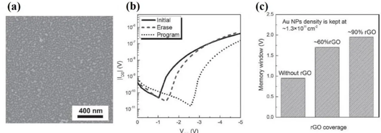
(36) Thèse de Shuo Li, Université de Lille, 2018. Chapter 1 State of the art voltage is applied to the control gate to inject electrons rom the channel into the NPs. The application of a reverse bias causes the reverse tunneling of electrons into the channel [85].. Figure 1.15 (a) Schematic of the program and erase operation in a NFGM device. A schematic band diagram illustrating (b) write and (c) erase processes in a Si based NFGM device [84].. 1.3.2 Nano-floating gate layers The nano-floating gate layer as the key device element in NFGM has been focused all the time during the research. The first formation of nanocrystal-based charge-trapping flash memory devices was reported by Tiwari et al [86], they used Si nanocrystals embedded in the gate oxide as the charge-storage element based on a conventional n-channel metal-oxidesemiconductor transistor, and the Si nanocrystals were synthesized by chemical vapor deposition. Since the early report, considerable progress has been made on the fabrication of nanocrystal-based memory over the years. Currently, for the charge floating gate, varied materials have been investigated to use for the charge-storing medium, for the medium that most commonly used, semiconductive or metallic nanoparticles that have been thermally deposited or chemically assembled [87], nanocomposites (e. g. Polymer/ZnO) [88, 89], carbonbased charge trapping materials (e. g. C60 or graphene) [90, 91]. 22 © 2018 Tous droits réservés.. lilliad.univ-lille.fr.
(37) Thèse de Shuo Li, Université de Lille, 2018. Chapter 1 State of the art In the kinds of the charge-storing medium, the metallic nanoparticles are the most widely used floating gate layer as the sample preparation process and easy to control the density of the particles. For example, figure 1.16(a-d) shows the TEM images of various metals NPs, including those of Au, Ag, Cu and Al, as a floating gate layer in NFGM devices that reported in Ref. [87]. The NPs were inserted between the bilayers of various polymer dielectrics (polystyrene (PS)/poly(4-vinyl phenol) (PVP) or PS/poly(methyl methacrylate (PMMA)). The effects of metallic NPs and gate dielectrics were investigated and compared in the literature, and the best performing P(NDI2OD-T2)-based NFGM devices were found as the ones fabricated using PMMA and Au NPs.. Figure 1.16 (a-d) TEM images of the various thermally deposited metallic NPs (1.0 nm thick deposited): (a) Au, (b) Ag, (c) Cu, and (d) Al. (e) Memory hysteresis loops and (f) corresponding memory windows of the transfer plots, Abs(Id) vs Vg at Vd=30 V, for the OFETs fabricated with various metallic NPs, i.e., those of Au, Ag, Cu and Al [87].. Furthermore, the 2D nanomaterial of graphene and derivative graphene like graphene oxide and its reduced form (rGO) have been adapted as charge trapping media for more efficient charge trapping but also better compatibility with solution processes. For example, Dai et al developed an organic nano-floating gate memory (NFGM) device using solution-processed graphite nanocrystals as nano-floating gate materials [92]. Mi Jung Lee et al fabricated an ntype charge-trapping memory device with rGO as the charge-trapping layer on the flexible 23 © 2018 Tous droits réservés.. lilliad.univ-lille.fr.
(38) Thèse de Shuo Li, Université de Lille, 2018. Chapter 1 State of the art substrate using all-solution processes [91]. Very Recently, Tae-Wook Kim et al demonstrated a graphene quantum dots (GQD)-based organic NFGM device using pentacene as the organic channel layer and PS as the tunneling layer [93]. Most of organic NFGMs exhibit relatively poor device characteristics along with markedly shorter retention times, therefore, the NFGM with double floating-gate were proposed to optimize the performances of NFGM devices [94-96]. For instance, S. T. Han et al reported a hybrid double floating-gate memory device by utilizing an rGO-sheet monolayer and an Au NP array as upper and lower floating gates, respectively. The rGO acts as buffer layer at the interface between the Au NPs and the pentacene and decreases the surface roughness, consequently enhancing the electrical characteristics of the DFG devices, as shown in figure 1.17 [94]. When keep the density of the Au NPs at ~1.3×1011 cm–2, rGO coverage at ~90%, the memory window of the DFG memory reaches the largest value of 1.75 V and retention time is up to 105.. Figure 1.17 (a) SEM image of self-assembled 15 nm Au NP monolayer with a density of around 1.3 ×1011cm–2, (b) Transfer characteristics of DFG memory device, (c) Memory window with respect to different densities of rGO while the density of the Au NPs is kept at ≈1.3×1011cm–2 [94].. 1.3.3 Pentacene based NFGM For fabrication of NFGM devices on rigid or flexible substrates, pentacene has been widely selected and studied as the active layer [92-104]. Over the years, many efforts have been devoted to optimizing the floating-gate layers. Besides the floating-gate layers, the blocking and tunneling dielectric layer also has a direct impact on memory performance of floating-gate OFET memory devices [103]. Examples of the research that reported very recently, M. D. Yi et al obtained the improvement of the NFGM devices with high density porous structure of PMMA tunneling layer that was mainly attributed to both the high charge capture and release 24 © 2018 Tous droits réservés.. lilliad.univ-lille.fr.
(39) Thèse de Shuo Li, Université de Lille, 2018. Chapter 1 State of the art efficiency and the high electrical insulating property [103]. Tae-Wook Kim et al used the method that one-step synthesis of Au NPs by simple annealing of the solid phase PAN and an Au salt to fabricate the NFGM and found the excellent performances of the memory, as shown in figure 1.18 [102]. The memory devices exhibited a high on/off ratio (over 106), large hysteresis windows (76.7 V), and stable endurance performances (3000 cycles). Otherwise, the multilevel charge storage phenomenon was also found in pentacene based NFGM. The multilevel transistor memories can be utilized to increase the memory capacity without decreasing the size of the device to the nanoscale [98].. Figure 1.18 (a) The device structure of the memory with p++ Si/SiO2/Au NPs in PAN/PS/pentacene/Au. (b) Transfer characteristics of NFGM. The transfer curves were measured by a gate double sweep with ranges of ±40 V and ±70 V at Vd =-20 V. (c) Endurance test results of the cyclic write-read-erase-read (W–R–E–R) test. (d) Retention time test results of the written state and erased state [102].. 25 © 2018 Tous droits réservés.. lilliad.univ-lille.fr.
(40) Thèse de Shuo Li, Université de Lille, 2018. Chapter 1 State of the art Considering the effects of materials and process conditions, the characteristics of the pentacene based NFGM were improved more or less that have been reported. Table 1-1 shows the summary of key characteristics of pentacene based FET memory devices that reported in the Refs in recent years.. Table 1-1. Summary of key characteristics of pentacene based NFGM devices that reported in the Refs in recent years. (P/E: Program/Erase) Charge store medium. VP/E (V). Mobility (cm2V-1s-1). Memory window (V). Ion/Ioff (V). P/E cycles. Retention time (s). Ref. Au NPs. ±90. 0.25. 10. ˃102. 700. 105. [97]. PET/Al2O3. Au NPs. ±50. -. 16.5. 3×10³. 1000. ˃105. [98]. PET/Al2O3. rGO sheets/. ±5. 0.1. .95. ~103. 1000. 105. [94]. ±5. 0.0125. 4.2. 8.3×10³. 500. 104. [96]. Substrate/ dielectrics PES/crosslinked PVP. Au NPs Glass/HfO2. CuPc NPs +N-C60. Si/SiO2/. Graphene. ±80. 0.061. ~40. 105. 110. ˃105. [99]. Si/SiO2. Ferritin NPs. ±100. 0.013. ˃20. 104. 200. 104 (˃107). [100]. ±45. 0.53. 18.7. ˃105. 600. 104. [101]. ±70. 0.809. 76.7. ˃106. 3000. ˃ 104. [102]. 0.49. 43. 105. 300s. 104. [103]. Si/SiO2. Si/SiO2 Si/SiO2/ Porous PMMA. Au NPs +Pt NPs S-PAN +Au NPs Au NPs. -120 /+80. From the summary of the characteristics of pentacene based NFGM devices that reported in recent years, we can see that most of the pentacene NFGM devices are fabricated on rigid substrates of silicon [96, 99-103], and the tunneling and blocking layers are mainly inorganic dielectrics like SiO2 and Al2O3, which needs relatively high temperature to deposit. For the flexible NFGM [94, 97, 98], only Ref. [97] used organic as the blocking layer, however, the operation voltage is very large (±90 V), the memory window is small, and the current on/off ratio is low. Hence, it signifies to develop new approach to improve the memory performances and the realization of flexible NFGM by using all organic materials are worth to going to research. 26 © 2018 Tous droits réservés.. lilliad.univ-lille.fr.
(41) Thèse de Shuo Li, Université de Lille, 2018. Chapter 1 State of the art. 1.4 Conclusions In this chapter, we describe the state of the art of OFET and NFGM and the motivation of this thesis is presented. In detail, the configurations and the operations of the OFET and the NFGM are presented first. Then, the typical high mobility organic semiconductors that used in OFET devices are represented. From the research of widely literatures and the point of commercial applications, the pentacene is chosen as the organic semiconductors to fabricate our OFET and NFGM devices in this thesis. Thus, the progress of pentacene based OFET and NFGM in recent years has been introduced. Finally, from the summery of the recent reports that involved of pentacene NFGM, the Au NPs and rGO sheets are chosen as the floating gate in this work, in addition, the dielectric materials and the structures were mainly taken into consideration for this work and our aim is to obtain high performances of OFET and NFGM on rigid and flexible substrates.. 27 © 2018 Tous droits réservés.. lilliad.univ-lille.fr.
(42) Thèse de Shuo Li, Université de Lille, 2018. Chapter 1 State of the art. References [1] C. D. Dimitrakopoulos, S. Purushothaman, J. Kymissis, A. Callegari, J. M. Shaw. Lowvoltage organic transistors on plastic comprising high-dielectric constant gate Insulators. Science, 1999, vol. 283, p. 822-824. [2] U. Zschieschang, H. Klauk, M. Halik, G. Schmid, C. Dehm, Flexible organic circuits with printed gate electrodes. Adv. Mater., 2003, vol. 15, p. 1147-1151. [3] H. Klauk, M. Halik, U. Zschieschang, F. Eder, G. Schmid, and C. Dehm. Pentacene organic transistors and ring oscillators on glass and on flexible polymeric substrates. Appl. Phys. Lett., 2003, vol. 82, p. 4175. [4] G. H. Gelinck, H. E. A. Huitema, E. V. Veenendaal, E. Cantatore, L. Schrijnemakers, J. B. P. H. van der Putten et.al.. Flexible active-matrix displays and shift registers based on solution-processed organic transistors. Nat. Mater., 2004, vol. 3, p. 106-110. [5] A. Dodabalapur. Organic and polymer transistors for electronics, Mater. Today, 2006, vol. 9, p. 24-30. [6] H. Sirringhaus. 25th Anniversary article: organic field-effect transistors: the path beyond amorphous silicon. Adv. Mater., 2014, vol. 26, p. 1319-1335. [7] H. L. Dong, X. L. Fu, J. Liu, Z. R. Wang, W. P. Hu. 25th Anniversary article: key points for high-mobility organic field-effect transistors. Adv. Mater., 2013, vol. 25, p. 6158-6182. [8] A. Dodabalapur, Z. Bao, A. Makhija, J. G. Laquindanum, V. R. Raju, Y. Feng, H. E. Katz, and J. Rogers, Organic smart pixels. Appl. Phys. Lett. 1998, vol. 73, p. 142. [9] B. Crone, A. Dodabalapur, A. Gelperin, L. Torsi, H. E. Katz, A. J. Lovinger, and Z. Bao. Electronic sensing of vapors with organic transistors. Appl. Phys. Lett., 2001, vol. 78, p. 2229. [10] M. D. Angione, R. Pilolli, S. Cotrone, M. Magliulo, A. Mallardi, G. Palazzo, L. Sabbatini, D. Fine, A. Dodabalapur, N. Cioffi, L. Torsi. Carbon based materials for electronic biosensing. Mater. Today 2011, vol. 14, p. 424-433. [11] E. Delamarche, M. Geissler, J. Vichiconti, W. S. Graham, P. A. Andry et. al.. Electroless deposition of NiB on 15 inch glass substrates for the fabrication of transistor gates for liquid crystal displays. Langmuir, 2003, vol. 19, p. 5923-5935. [12] P. Gkoupidenis, N. Schaefer, B. Garlan and G. G. Malliaras. Neuromorphic functions in PEDOT:PSS organic electrochemical transistors. Adv. Mater., 2015, vol. 27, p. 7176-7180. [13] C. H. Kim, S. J. Sung and M. H. Yoon. Synaptic organic transistors with a vacuumdeposited charge-trapping nanosheet. Sci. Rep., 2016, vol. 6, p. 1-8. [14] P. Heremans, G. H. Gelinck, R. Muller, K. J. Baeg, D. Y. Kimand Y. Y. Noh. Polymer and organic nonvolatile memory devices. Chem. Mater., 2010, vol. 23, p. 341-358. [15] W. Wang, K. L. Kim, S. M. Cho, J. H. Lee, and C. Park. Nonvolatile Transistor Memory with Self-Assembled Semiconducting Polymer Nanodomain Floating Gates. ACS Appl. Mater. Interfaces, 2016, vol. 8, p. 33863-33873. [16] J. Li, C. Zhang, L. Duan, L. M. Zhang, L. D. Wang, G. F. Dong and Z. L. Wang. Flexible Organic Tribotronic Transistor Memory for a Visible and Wearable Touch Monitoring System. Adv. Mater., 2016, 28, p. 106-110. 28 © 2018 Tous droits réservés.. lilliad.univ-lille.fr.
(43) Thèse de Shuo Li, Université de Lille, 2018. Chapter 1 State of the art [17] N. Keltouma, F. Mohammed and A. Saghir. Design and characterization of tapered transition and inductive window filter based on Substrate Integrated Waveguide technology (SIW). International Journal of Computer Science Issues, 2011, vol. 8, p. 135138. [18] Z. T. Liu, C. Lee, V. Narayanan, G. Pei, E.C. Kan. Metal nanocrystal memories. I. Device design and fabrication. IEEE Trans. Electron. Devices, 2002, vol. 49, p. 1606-1613. [19] S. Moller, C. Perlov, W. Jackson, C. Taussig, S.R. Forrest. A polymer/semiconductor write-once read-many-times memory. Nature, 2003, vol. 426, p. 166-169. [20] R. J. Tseng, J. Huang, J. Ouyang, R. B. Kaner, Y. Yang. Polyaniline Nanofiber/Gold Nanoparticle Nonvolatile Memory. Nano. Lett., 2005, vol. 5, p. 1077-1080. [21] K. -J. Baeg, Y. -Y. Noh, J. Ghim, B. Lim, D.-Y. Kim. Polarity Effects of Polymer Gate Electrets on Non-Volatile Organic Field-Effect Transistor Memory. Adv. Funct. Mater., 2008, vol. 18, p. 3678-3685. [22] R. Waser, R. Dittmann, G. Staikov, K. Szot. Redox-based resistive switching memoriesnanoionic mechanisms, prospects, and challenges. Adv. Mater., 2009, vol. 21, p. 26322663. [23] M. H. White, D. A. Adams, J. K. Bu. On the go with SONOS. IEEE Circuits Devices, 2000, vol. 16, p. 22-31. [24] J. S. Lee. Recent progress in gold nanoparticle-based non-volatile memory devices. Gold Bull., 2010, vol. 43, p. 189-199. [25] Y. Yoshimitsu, K. Yoshinari, M. Toshimasa. Scalable Virtual-Ground Multilevel-Cell Floating-Gate Flash Memory. IEEE Trans. Electron. Devices, 2013, vol. 60, p. 2518-2524. [26] J. S. Lee. Progress in non-volatile memory devices based on nanostructured materials and nanofabrication. J. Mater. Chem., 2011, vol. 21, p. 14097-14112. [27] J. S. Lee, C. S. Kang, Y. C. Shin, C. H. Lee, K. T. Park, J. S. Sel et. al.. Data Retention Characteristics of Nitride-Based Charge Trap Memory Devices with High-k Dielectrics and High-Work-Function Metal Gates for Multi-Gigabit Flash Memory. Jpn. J. Appl. Phys. Part 1, 2006, vol. 45, 3213-3216. [28] J. S. Lee. Review Paper: Nano-Floating Gate Memory Devices. Electron. Mater. Lett., 2011, vol. 7, p. 175-183. [29] E. Kapetanakis, P. Normand, D. Tsoukalas, K. Beltsios, J. Stoemenos, S. Zhang, J. van den Berg, Charge storage and interface states effects in Si-nanocrystal memory obtained using low-energy Si+ implantation and annealing. Appl. Phys. Lett., 2000, vol. 77, p. 34503452. [30] J. De Blauwe. Nanocrystal nonvolatile memory devices. IEEE Trans. Nanotechnol., 2002, vol. 1, p. 72-77. [31] G. Gelinck. Semiconductor electronics: Trapped fast at the gate. Nature, 2007, vol. 445, p. 268-270. [32] Hagen Klauk. Organic thin-film transistors. Chem. Soc. Rev., 2010, vol. 39, p. 2643-2666. [33] Cap. Eng. Mustafa Fayez Ahmed. Manufacturing and Modeling of an Organic Thin Film Transistor. Ph.D thesis. 2016.. 29 © 2018 Tous droits réservés.. lilliad.univ-lille.fr.
Figure

![Figure 1.10 Three examples for rate-dependent morphology in thick pentacene films are given in the upper row AFM height micrographs, 5 μm × 5 μm [68]](https://thumb-eu.123doks.com/thumbv2/123doknet/3642482.107331/30.892.127.760.886.1084/figure-examples-dependent-morphology-pentacene-upper-height-micrographs.webp)

+7


Documents relatifs
Finally, the regression analysis was performed at the given pressure levels, using the following proxies: (1) two trend terms (identical to the method described earlier as the
Abbréviations: HSC, hemopoietic stem cell; MPP, multipotent progenitors; CMP, common myeloid precursors; CLP, common lymphoid precursors; GMP, granulocyte and macrophage
Un transistor organique à effet de champ dont un exemple est présenté sur la Figure I-3. a), est constitué d’une couche de semi-conducteur organique en contact
The importance and the implications of recombination on the evolution of NoV were studied in natural conditions and in experimental conditions throughout this thesis. Three
They agree on the insufficiency of the written tests, and they regard that they need to be exposed to oral tests, for they were all the time exposed to oral aspects of language,
Keywords: 3D Heterogeneous Integration, Nano-Objects, Flexible Substrate, Flex Assembly, Wireless sensor
L'AAMR « va en ce sens» puisqu'elle propose une évaluation multidimensionnelle qui exige une compréhension plus poussée des multiples facteurs pouvant causer une
Is the development of commercial livestock farms and intensive family farms leading to a phenomenon of agricultural specialization of production systems.. How can this
