Département de génie électrique
LASER INDUCED QUANTUM WELL
INTERMIXING: REPRODUCIBILITY STUDY AND
FABRICATION OF SUPERLUMINESCENT DIODES
INTERDIFFUSION DE PUITS QUANTIQUES
INDUITE PAR LASER: ÉTUDE DE LA
REPRODUCTIBILITÉ ET FABRICATION DE
DIODES SUPERLUMINESCENTES
Thèse de doctorat Spécialité : génie électrique
Romain BEAL
Jury : Jan J. DUBOWSKI (directeur) Vincent AIMEZ (codirecteur) Simon FAFARD (rapporteur) Amr S. HELMY (examinateur) Philip POOLE (examinateur)
« Ignoranti quem portum petat nullus suus uentus est. »
i
SUMMARY
Photonic Integrated Circuits (PIC) are of tremendous interest for photonics system in order to reduce their power consumption, size, fabrication cost and improve their reliability of fiber optics linked discrete component architecture. However, unlike for microelectronics, in photonics different heterostructures are required depending on the type of device (laser sources, detectors, modulators, passive waveguides…). Therefore photonics integration needs a technology able to produce multiple bandgap energy wafers with a suitable final material quality in a reproducible manner and at a competitive cost: a technological challenge that has not been completely solved yet.
Quantum Well Intermixing (QWI) is a post growth bandgap tuning process based on the localized and controlled modification of quantum well composition profile that aims to address these matters. UV laser induced QWI (UV-Laser-QWI) relies on high power excimer laser to introduce point defects near the heterostructure surface. By adjusting the laser beam shape, position, fluence and the number of pulse delivered, the different regions to be intermixed can be defined prior to a rapid thermal annealing step that will activate the point defects diffusion across the heterostructure and generate quantum well intermixing. UV-Laser-QWI presents the consequent advantage of allowing the patterning of multiple bandgap regions without relying on photolithographic means, thus offering potentially larger versatility and time efficiency than other QWI processes.
UV-Laser-QWI reproducibility was studied by processing samples from an InGaAs/InGaAsP/InP 5 quantum well heterostructure emitting at 1.55 µm. 217 different sites on 12 samples were processed with various laser doses. The quantum well intermixing generated was then characterized by room temperature photoluminescence (PL) mapping. Under those experimental conditions, UV-Laser-QWI was able to deliver heterostructures with a PL peak wavelength blue shift controlled within a +/- 15 % range up to 101.5nm. The annealing temperature proved to be the most critical parameter as the PL peak wavelength in the laser irradiated areas varied at the rate of 1.8 nm per degree Celsius. When processing a single wafer, thus limiting the annealing temperature variations, the bandgap tuned regions proved to be deliverable within ± 7.9%, hence establishing the potential of UV-Laser-QWI as a reproducible bandgap tuning solution.
ii
their influence on the SLDs’ performances was measured. The most favorable bandgap modifications for the delivery of a very broadband emitting SLD were analyzed, as well as the ones to be considered for producing devices with a flat top shaped spectrum. The intermixed SLDs spectra reached full width at half maximum values of 100 nm for a relatively flattop spectrum which compare favorably with the ≈ 40nm of reference devices at equal power. The light-intensity characteristics of intermixed material made devices were very close to the ones of reference SLD made from as-grown material which let us think that the alteration of material quality by the intermixing process was extremely limited. These results demonstrated that the suitability of UV-Laser-QWI for concrete application to photonic devices fabrication. Finally, an alternative laser QWI technique was evaluated for SLD fabrication and compared to the UV laser based one. IR-RTA relies on the simultaneous use of two IR laser to anneal local region of a wafer: a 980 nm laser diode coupled to a pigtailed fiber for the wafer background heating and a 500 µm large beam TEM 00 Nd:YAG laser emitting at 1064 nm to anneal up to intermixing temperature a localized region of the wafer. The processed samples exhibited a 33 % spectral width increase of the spectrum compare to reference device at equal power of 1.5 mW. However, the PL intensity was decreased by up to 60 % in the intermixed regions and the experiments proved the difficulty to avoid these material degradations of material quality with IR-RTA.
Keywords : Quantum well intermixing, superluminescent diode, optoelectronics, photonics,
iii
RÉSUMÉ
L’intégration de circuit photonique vise à réduire la consommation énergétique, la taille, le coût et les risques de panne des systèmes photoniques traditionnels faits de composants distincts connectés par fibre optique. Cependant, contrairement à la microélectronique, des hétérostructures spécifiques sont requises pour chaque composant : lasers, détecteurs, modulateurs, guides d’ondes… De cette constatation découle le besoin d’une technologie capable de produire des gaufres d’hétérostructures III/V de qualité à plusieurs énergies de gap, et ce de façon reproductible pour un coût compétitif. Aucune des techniques actuelles ne répond pour l’instant pleinement à tous ces impératifs.
L’interdiffusion de puits quantique (IPQ) est un procédé post épitaxie basé sur la modification locale de la composition des puits quantiques. L’IPQ induite par laser UV (IPQ-UV) est basée sur l’utilisation de laser excimer (Argon-Fluor émettant à 193 nm ou Krypton-Fluor à 248 nm) pour introduire des défauts ponctuels à la surface de l’hétérostructure. En ajustant la taille du faisceau, sa position, son énergie ainsi que le nombre d’impulsions laser délivrées à la surface du matériau, on peut définir les régions à interdiffuser ainsi que leur futur degré d’interdiffusion. Un recuit de la gaufre active ensuite la diffusion des défauts et par conséquent l’interdiffusion du puits. L’IPQ-UV présente l’avantage considérable de se passer de photolithographie pour définir les zones de différentes énergies de gap, diminuant ainsi la durée et potentiellement le coût du procédé.
La reproductibilité de l’IPQ-UV a été étudiée pour l’interdiffusion d’une structure à 5 puits quantiques d’InGaAs/InGaAsP/InP émettant à 1.55 µm. 217 régions sur 12 échantillons ont été irradiés par un laser KrF avec des nombres d’impulsion variables selon les sites et avec une densité d’énergie constante de 155 mJ/cm². Les modifications de la structure générée par ce traitement furent ensuite mesurées par cartographie en photoluminescence (PL) à température ambiante. L’analyse des données montra que l’IPQ-UV permet un contrôle du décalage vers le bleu du pic de PL à +/- 15 % jusqu’à 101.5nm. La température du recuit est apparue comme le paramètre crucial du procédé, puisque la longueur d’onde du pic de PL des zones interdiffusées varie de 1.8 nm par degré Celsius. En considérant les sites irradiés sur une seule gaufre, c’est à dire en s’affranchissant des variations de température entre deux recuits de notre système, la variation du pic de PL est contrôlable dans une plage de ± 7.9%. Ces
iv
résultats démontrent le potentiel de l’IPQ-UV en tant que procédé reproductible de production de gaufre à plusieurs énergies de gap.
L’IPQ-UV a été utilisé pour la fabrication de diodes superluminescentes (DSLs). Différents type de structure à énergie de gap multiple ont été testés et leurs influences sur les performances spectrales des diodes évalués. Les spectres des DSLs faites de matériau interdiffusé ont atteint des largeurs à mi-hauteur dépassant les 100 nm (jusqu’à 132 nm), ce qui est une amélioration conséquente des ≈ 40nm des DSLs de référence à puissance égale. Les caractéristiques intensité–courant des DSLs interdiffusés furent mesurées comme étant très proches de celle des dispositifs de référence faits de matériau brut, ce qui suggère que l’IPQ-UV n’a pas ou très peu altéré la qualité du matériau initial. Ces résultats prouvent la capacité de l’IPQ-UV à être utilisé pour la fabrication de dispositifs photoniques.
Une technique alternative d’IPQ par laser a été évaluée et comparée à l’IPQ-UV pour la fabrication de DSL. Le recuit rapide par laser IR est basé sur l’utilisation simultanée de deux lasers IR pour chauffer localement l’hétérostructure jusqu’à une température suffisante pour provoquer l’interdiffusion: une diode laser haute puissante émettant à 980 nanomètre couplée dans une fibre chauffe la face arrière de la gaufre sur une large surface à une température restant inférieure à celle requise pour provoquer l’interdiffusion et un laser Nd:YAG TEM 00 émettant à 1064 nm un faisceau de 500 µm de large provoque une élévation de température additionnelle localisée à la surface de l’échantillon, permettant ainsi l’interdiffusion de l’hétérostructure. Les dispositifs fabriqués ont montré une augmentation de 33 % de la largeur à mi-hauteur du spectre émis à puissance égale de 1.5 mW. Cependant, l’intensité du pic de PL dans les zones interdiffusés est diminuée de 60 %, suggérant une dégradation du matériau et la difficulté à produire un matériau de qualité satisfaisante.
Mots-clés : Interdiffusion de puits quantique, diode superluminescente, optoélectronique,
v
REMERCIEMENTS
Je remercie Monsieur Simon Fafard, professeur à l’Université de Sherbrooke pour avoir accepté d’être le rapporteur de cette thèse. Je remercie également messieurs Amr S. Helmy, professeur à l’Université de Toronto et Philip Poole, du Conseil national de recherches Canada de bien avoir accepté de faire partie du jury et d’évaluer les travaux de cette thèse.
Je remercie infiniment mes directeurs, Jan J. Dubowski et Vincent Aimez pour leur apport et leurs conseils tout au long de l’aventure que fut ce doctorat.
Je remercie bien sûr mes parents et mes frères pour leur soutien indéfectible.
L’équipe du CRN2 puis du 3IT.nano, professionnels de recherche et techniciens, ont été d’une assistance plus que précieuse, mes remerciements vont plus particulièrement à: Jean Beerens, Guillaume Bertand, Daniel Blackburn, Mélanie Cloutier, Marie-Josée Gour, Étienne Grondin, Abdelatif Jaouad, René Labrecque, Michael Lacerte, Pierre Lafrance, Pierre Langlois, Denis Pellé et Caroline Roy. Un grand merci également à Danielle Gagné, secrétaire de direction au département de Génie Électrique pour sa disponibilité et son efficacité.
Je n’oublie pas mes collègues qui ont permis une ambiance agréable au cours de cette thèse et notamment Maxence Mounier, Guillaume Beaudin, Simon Geissbuehler, Rym Feriel Leulmi, Sarah Farhi, Maïté Volatier-Ravat, Alvaro Jiménez, Osvaldo Arenas, Ahmed Chakroun, Abdelaziz Ramzi, Mohamed Walid Hassen et Thibaut Barreteau. Je souhaite également exprimer ma gratitude à mes collègues Khalid Moumanis, Jonathan Genest, Neng Liu et Radoslaw Stanowski pour les discussions enrichissantes que nous avons eues.
Enfin, les amis que j’ai eu le privilège de côtoyer durant mon séjour à Sherbrooke et plus particulièrement Marie Champagne, Martin Blouin, Jean Théberge, Pauline Fayein, Christian Thibaudeau, Adriana Lions et Marc-André Hachey.
Il est impossible de conclure ces remerciements sans avoir une pensée pour le café, qui fut le carburant principal de la rédaction de cette thèse, parfois à la limite de la tachycardie.
vii
TABLE OF CONTENTS
SUMMARY i RÉSUMÉ iii REMERCIEMENTS ... v LIST OF FIGURES ... xiLIST OF TABLES ... xix
LIST OF ACRONYMS ... xxi
CHAPTER 1 Introduction ... 1
CHAPTER 2 Photonics integration state of the art ... 5
2.1 Theory of semiconductor-light interactions ... 5
2.1.1 AIII-BV semiconductor band structure and electronic states ... 5
2.1.2 Semiconductor heterostructure ... 8
2.2 AIII-BV semiconductor integration for photonics application ... 9
2.2.1 Motivations ... 9
2.2.2 Hybrid integration ... 11
2.2.3 Monolithic integration ... 12
(1) Selective area growth ... 13
(2) Butt joint regrowth ... 14
(3) Vertical integration techniques ... 14
(4) Polarisation based Integration Scheme ... 16
2.3 Quantum well intermixing ... 16
2.3.1 General principles ... 17
2.3.2 Impurity induced disordering ... 19
2.3.3 Impurity free vacancy disordering ... 21
2.3.4 Universal damage technique ... 22
2.3.5 Plasma induced quantum well intermixing ... 23
2.3.6 Ultraviolet laser induced quantum well intermixing ... 23
2.3.7 CW infrared laser induced quantum well intermixing ... 25
2.3.8 Pulsed infrared laser induced quantum well intermixing ... 26
2.4 Quantum well intermixing applications ... 26
2.5 Superluminescent diodes ... 29
2.5.1 General device characteristics ... 29
2.5.2 Applications ... 30
2.5.3 Superluminescent diode spectrum broadening ... 32
Chirped quantum wells ... 33
Self-assembled quantum dot heterostructure ... 34
Quantum well intermixing ... 35
Multi section devices ... 37
2.6 Summary ... 39
CHAPTER 3 UV Laser induced quantum well intermixing ... 41
3.1 Experimental set up ... 41
3.3 UV Laser induced Quantum Well Intermixing ... 47
3.4 Application to device fabrication: intermixed material made laser diodes ... 53
3.5 Comparison with other intermixing processes ... 54
3.6 Summary ... 56
CHAPTER 4 UV-Laser-QWI: process practicality ... 59
4.1 Excimer laser induced quantum well intermixing: a reproducibility study of the process for fabrication of photonic integrated devices ... 59
4.1.1 Abstract ... 59
4.1.2 Introduction ... 60
4.1.3 Experimental details ... 62
4.1.4 Results and discussion ... 64
4.1.5 Conclusion ... 69
4.1.6 Acknowledgments ... 70
4.2 Additional considerations on UV-QWI reproducibility ... 70
4.2.1 Detailed analysis of experimental results ... 70
4.2.2 RTA system limitations ... 73
4.2.3 Laser fluence variations ... 76
4.2.4 Laser repetition rate influence ... 79
4.3 Same site blue-shift variations ... 81
4.4 Summary ... 84
CHAPTER 5 Enhanced spectrum superluminescent diode prototyping by UV QWI ... 87
5.1 Introduction ... 87
5.2 Theoretical consideration ... 87
5.2.1 Output spectrum ... 88
5.2.2 Analysis for multi-bandgap SLD conception ... 90
5.3 SLD prototyping: preliminary devices ... 91
5.3.1 Two bandgap energy devices ... 92
5.3.2 Three bandgap energy devices ... 93
5.4 UV laser quantum well intermixing based prototyping of bandgap tuned heterostructures for the fabrication of superluminescent diodes ... 95
5.4.1 Abstract ... 95
5.4.2 Introduction ... 96
5.4.3 Experimental details ... 97
(1) UV-Laser-QWI ... 97
(2) Devices fabrication and test conditions ... 99
5.4.4 Results and discussion ... 101
(1) Sample A devices ... 101
ix
5.4.5 Conclusion ... 105
5.4.6 Acknowledgments ... 106
5.5 Electrical characteristics ... 106
5.6 Summary ... 107
CHAPTER 6 Comparison with IR Laser QWI fabricated SLDs ... 109
6.1 Infrared laser rapid thermal annealing ... 109
6.1.1 Experimental procedure ... 109
(1) Laser system ... 110
(2) Measurement and process control ... 111
6.1.2 IR Laser induced QWI ... 112
6.2 IR-Laser-QWI: Preliminary results ... 113
6.2.1 Bandgap gradient creation using a single 980 nm laser diode source ... 113
6.2.2 Evaluation of IR-Laser-QWI parameters satisfying for the fabrication of optoelectronics devices ... 116
(1) Slow speed scanning process ... 116
(2) Fast speed scanning process ... 118
6.3 Enhanced Spectrum Superluminescent Diodes Fabricated by Infrared Laser Rapid Thermal Annealing ... 121 6.3.1 Abstract ... 121 6.3.2 Introduction ... 121 6.3.3 Experimental details ... 124 (1) Material ... 124 (2) Photoluminescence characterization ... 126
(3) Superluminescent diodes fabrication ... 126
(4) Superluminescent diodes test procedure ... 127
6.3.4 Results and discussion ... 127
6.3.5 Conclusion ... 132
6.3.6 Acknowledgments ... 133
6.4 Analysis of SLDs electrical characteristics... 133
6.5 Comparison of IR and UV laser induced QWI abilities ... 134
6.5.1 Technological complexity ... 134
6.5.2 Reproduciblity ... 134
6.5.3 Material suitability for PIC fabrication ... 135
CHAPTER 7 Conclusions and perspectives ... 137
7.1 Conclusions ... 137
7.2 Perspectives and future works ... 138
xi
LIST OF FIGURES
Figure 1.1 Requirements for data transfer and available technologies [G. Lifante, 2003] ... 2 Figure 1.2 Used international bandwidth and projection over the decade [J. Brodkin, 2012] .... 2 Figure 2.1 Occupation states for: (a)(b) Metals, (c) Semiconductor and (d) Insulator (CB: Conduction Band and VB: Valence Band) [C.F. Klingshirn, 2007] ... 5 Figure 2.2 Energy band diagrams and major carrier transition processes in indium phosphide (direct bandgap) and silicon (indirect bandgap) crystals [D. Liang, J.E. Bowers, 2010] ... 6 Figure 2.3 The variation of lattice constant with band gap for the III–V ternary compounds. The direct gap materials are shown with the solid line and the indirect gap material – with the dashed line [B. Tabbert, A. Goushcha, 2012] ... 7 Figure 2.4 The three electron–photon interactions in semiconductors: (a) spontaneous emission, (b) stimulated absorption, and (c) stimulated emission [S. Kasap, P. Capper, 2007] . 8 Figure 2.5 Various geometries of quantum wells active region, (i) single QW(separate confinement heterostructure, SCH), (ii) multiple QWSCH, and (c) GRINSCH (graded-index SCH) structure. (b) Layer sequence for a separate confinement heterostructure laser [M. Grundmann, J.H. Weaver, 2007] ... 9 Figure 2.6 The different building pieces that can and need to be integrated on a same chip to provide a complete efficient Photonic Integrated Circuit (PIC) [L.A. Coldren, 2008] ... 10 Figure 2.7 Historical trend and timeline for monolithic photonic integration on InP. The vertical scale indicating the number of component is linear, and the red filled circles start at 1 and go to 240. [R. Nagarajan et al., 2010] ... 11 Figure 2.8 Various techniques for achieving active and passive sections orthogonal to the growth direction [J.W. Raring, L.A. Coldren, 2007]... 12 Figure 2.9 Selective area epitaxy process, (a) Schematic diagram of a MQW wavelength-tunable DBR laser with monolithically integrated external cavity EA modulator. (b) Schematic diagram of the dual oxide stripe mask used during the selective growth of the active region for the device [J.J. Coleman et al., 1997] ... 13 Figure 2.10 Cross-section schematic of a butt-coupled region of integrated amplifier [J. Wallin et al., 1992] ... 14 Figure 2.11 A prospective GaInAsP Integrated Twin Guide laser with three-dimensional output guide [K. Iga et al., 1979] ... 15
Figure 2.12 Illustration of the intermixing process for a GaAs/AlGaAs quantum well: on the left the QW prior to intermixing, on the right after intermixing, some Aluminium has mixed into the QW and increased its gap energy [Intense, 2013] ... 17 Figure 2.13 Schematic illustration of diffusion mechanisms. (a)Top: exchange mechanism, bottom: ring mechanism. (b) Vacancy mechanism. (c) Interstitial mechanism. (d) Interstitialcy mechanism. (e) Substitutional-interstitial mechanisms, top: Frank-Turnbull mechanism, bottom: kick-out mechanism [U.W. Pohl, 2013] ... 18 Figure 2.14 Schematic of arsenic implantation through a graded SiO2 mask [S.L. Ng et al., 2003] ... 21 Figure 2.15 Multi bandgap ion implantation quantum well intermixing process: four bandgap regions were obtained. (a) Phosphorous ion implant into InP buffer with SiONx mask to preserve as-grown bandgap 1. (b) Diffusion of vacancies through quantum wells and barriers during RTA to create bandgap 2. (c) Selective removal of InP buffer layer to stop intermixing. (d) Diffusion of vacancies through QW structure for bandgap 3. (e) Selective removal of InP buffer and anneal for bandgap 4. (f) Blanket removal of InP buffer layer to planarize surface. [S.R. Jain et al., 2011] ... 21 Figure 2.16 Example of dielectric capping to control quantum well intermixing [B S Ooi et al., 1995]: the SiO2 layer promotes the interdiffusion while the SrF2 layer prevents it. ... 22 Figure 2.17 Schematic diagram of the Laser Rapid Thermal Annealing setup, Photoluminescence map of the IR-Laser-QWI processed In- GaAsP/InP QW sample with a ‘watermark’ of the QWI material [R. Stanowski, J.J. Dubowski, 2008] ... 26 Figure 2.18 Schematic of a laser with cold mirrors as fabricated by Intense Photonics [Intense, 2013] ... 27 Figure 2.19 Schematic diagram of a “generic” PIC: laser diode is coupled with an electro-absorption modulator and the output is directed into a low loss-waveguide splitter. The optimum operation of this PIC requires a different bandgap energy for each component [S. Charbonneau et al., 1998] ... 27 Figure 2.20 Typical spectra of different light emitting devices Source: Light-Emitting Diodes [E.F. Schubert, 2002] ... 30 Figure 2.21 Example of band structure of a chirped quantum-well [C.-F. Lin, B.-L. Lee, 1997] ... 33
xiii
Figure 2.22 Emission from a SLD made from chirped quantum well heterostructure at
different injection currents [B. Wu et al., 2000] ... 33
Figure 2.23 Size distribution and emission spectra of ideal and real QD ensembles [Z.Y. Zhang et al., 2010] ... 34
Figure 2.24 Broad band light emitting device obtain by Selective Area Epitaxy. Left: Dielectric mask used during structure growth and regions used for devices fabrication. Right: Resulting emitted spectrum [M.L. Osowski et al., 1994] ... 35
Figure 2.25 Left: schematic diagram of dielectric profile and bandgap energy profile in QW region created through one-step. Right: Output spectral of non-intermixed and intermixed superluminescent diode at ~1.7 mW output power [Y. Lam et al., 2003] ... 36
Figure 2.26 This consisted of a 200nm TiO2 film covered region, a 200nm SiO2 film covered region and a 500nm SiO2 film covered [K.J. Zhou et al., 2012] ... 36
Figure 2.27 CW EL spectra for various drive currents in a multi-section device [P.D.L. Judson et al., 2009] ... 38
Figure 2.28 3D overview of the III–V-on-silicon waveguide made broadband LED [A. De Groote et al., 2014] ... 38
Figure 3.1 Gas discharge section in an excimer laser tube ... 42
Figure 3.2 Left: Köhler Integrator (imaging homogenizer): Two microlens arrays LA1 and LA2, one condenser lens FL. Right: simulation of superposition in object plane for two identical microlens arrays consisting of N x N identical lenses. [R. Voelkel, K. Weible, 2008] ... 43
Figure 3.3 Left: ArF Laser beam profile measured at laser output. Right: ArF laser beam profile measured at first focal plan (after beam homogenization)... 43
Figure 3.4 Excimer laser irradiation set up schematic ... 44
Figure 3.5 Irradiated 100 µm large spots irradiated at different z axis position. The focal point corresponds to extreme left spot, and the distance from this point increases from left to right. The defects visible in two corners of the left spot were present on the mask ... 44
Figure 3.6 Rapid Thermal Processor JIPELEC JetFirst 100 ... 45
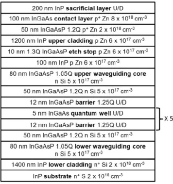
Figure 3.7 Multi quantum well structure M0062 ... 46
Figure 3.8 Multi quantum well structure M1580 ... 46
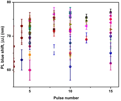
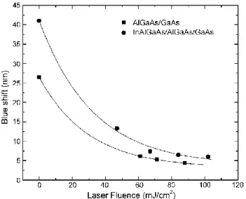
Figure 3.10 Blue shift in as-grown and 1000 pulse laser irradiated AlGaAs/GaAs (squares) and InAlGaAs/AlGaAs/GaAs (circles) samples after RTA at 900°C for 30 seconds [J. Genest et al., 2007] ... 48 Figure 3.11 Left: RT PL map of an ArF laser irradiated InGaAs/InGaAsP/InP QW structure after RTA at 725°C for 120 seconds. The upper and lower numbers correspond to the number of laser pulses and blueshift amplitude, respectively. Right: Variation of PL blueshift as a function of pulse number delivered by the ArF laser at 68, 75, 90 and 150 mJ/cm2. Solid lines are theoretically calculated values, squares are experimental data [Jonathan Genest et al., 2008] ... 49 Figure 3.12 Net PL blue shift as function of annealing duration in the laser irradiated sites of a laser QW heterostructure (A1, A2) and a shallow well QW heterostructure (B1,B2) [Neng Liu, 2013] ... 50 Figure 3.13 Absorption (left) and reflectance (right) spectra of InP [D.E. Aspnes, A. Studna, 1983] ... 51 Figure 3.14 Dependence of XPS atomic concentration of InP and surface adsorbates on the laser pulse number in samples irradiated with ArF laser in DI water (a), in air (b) and after RTA of the sample irradiated in DI water (c) and in air (d). [Neng Liu, J.J. Dubowski, 2013] 52 Figure 3.15 TOF-SIMS oxygen concentration depth profile in as grown sample, and in samples irradiated with ArF laser in DI water and in air before (a) and after (b) RTA at 700◦C for 2 min [Neng Liu, J.J. Dubowski, 2013] ... 52 Figure 3.16 Broad area injection laser diode spectra from intermixed and as-grown material [Jonathan Genest, 2008] ... 53 Figure 3.17 Comparison of as-grown and intermixed laser diode LI characteristics [Jonathan Genest, 2008] ... 54 Figure 4.1 Cross-section of the 5-QW laser heterostructure employed for a reproducibility study of the UV-Laser-QWI process ... 63 Figure 4.2 (a) PL blue shift as a function of pulse number for samples irradiated at 155 mJ/cm2. The results shown with the same style symbols identify the sites processed on the same sample. (b) Average values of PL blue shift (δblue) collected as a function of pulse number (only data for minimum 4 sites irradiated under the nominally same conditions are taken into account) ... 66
xv
Figure 4.3 Distribution of the |Δλ| values for the unirradiated material (red columns) and samples irradiated with 4-15 pulses (green columns) and 50-70 pulses (blue columns) ... 67 Figure 4.4 PL determined blue shift as a function of the RTA temperature for as-received material (◼) and sites annealed with 20 (●) and 60 (▲) pulses ... 68 Figure 4.5 Distribution of the |Δλ| values for two samples irradiated at 34 sites with 15 pulses (green columns) and 30 sites with 50-70 pulses (blue columns) respectively ... 69 Figure 4.6 PL Blue shift values measured for laser doses from 0 to 80 pulses at 155 mJ/cm² fluence, an exponential fit curve is added (green dashes) ... 71 Figure 4.7 PL Blue shift values measured for laser doses from 0 to 4 pulses at 155 mJ/cm² fluence after annealing at 670°C ... 71 Figure 4.8 PL Blue shift values measured for laser doses from 4 to 15 pulses at 155 mJ/cm² fluence (first saturation plateau) after annealing at 670°C ... 72 Figure 4.9 PL Blue shift values measured for laser doses from 15 to 50 pulses at 155 mJ/cm² fluence after annealing at 670°C ... 72 Figure 4.10 PL Blue shift values measured for laser doses from 50 to 70 pulses at 155 mJ/cm² fluence (second saturation plateau) after annealing at 670° ... 73 Figure 4.11 Left: photoluminescence peak wavelength mapping of sample processed in 34 sites with 15 pulses of KrF laser at 155 mJ/cm² fluence; right: cross section of the same PL Map illustrating the blue shift variation across sample width along the direction indicated by a double arrow on the left figure ... 74 Figure 4.12 Photoluminescence peak wavelength mapping of sample processed in 30 sites with 60 pulses of KrF laser at 155 mJ/cm² fluence ... 74 Figure 4.13 Position on the RTA support wafer of the different test samples and the thermocouple ... 75 Figure 4.14 Comparison of the blue shift of two samples irradiated with different pulse number at a 155 mJ/cm² laser fluence and annealed for 2 minutes with a 5°C variation ... 76 Figure 4.15 Left: Evolution of pulse laser fluence for the KrF laser; right: focus on the last 60 pulses measured ... 77 Figure 4.16 PL blue shift as a function of laser fluence for samples A and B for 5 and 50 pulses laser doses ... 78
Figure 4.12 Blue shift as a function of pulse number for 157 mJ/cm² and 245 mJ/cm² (all data coming from a single sample designated J792A) ... 79 Figure 4.18 PL map of the samples used for repetition rate influence on UV-Laser-QWI study. The reference 2 Hz sites are unframed on each sample, the other sites are framed with line of different color and style: dashed black line: 20 Hz, solid black line: 50 Hz, dashed red line: 60 Hz, solid red line: 80 Hz, dash-dot black line: 100 Hz. The number of KrF laser pulses delivered at 155 mJ/cm² fluence in air is indicated on each site. ... 80 Figure 4.19 Photoluminescence peak wavelength in site variation as a function of pulse number for samples irradiated with a 155 mJ/cm² laser fluence and annealed at 670°C for 2 minutes ... 82 Figure 4.20 Evolution of PL blue shift profile for a circular irradiated site ... 84 Figure 5.1 a) Schematic example of a multi bandgap broadband superluminescent diode; b) Output spectrum for the equal combination of three bandgap region (not taking into consideration the absorption and gain occurring through the waveguiding direction); c) actual output spectral shape that would result from such device ... 88 Figure 5.2 Illustration of a large difference between the rear emitting section and the front section gain peak wavelength ... 91 Figure 5.3 PL peak wavelength profile of the two bandgap energies device obtained by UV-Laser-QWI ... 93 Figure 5.4 Left: Maximum width Emitted spectrum of the 1.5 mm long SLD made from the material described in Figure 5.3; Right: Evolution of the emitted spectrum of the SLD for different injected current values ... 93 Figure 5.5 PL peak wavelength profile of the 3-bandgap energies structure obtained by UV-Laser-QWI ... 95 Figure 5.6 Maximum width output spectrum of the SLD made from the 3 bandgap energies structure presented in Figure 5.5 ... 95 Figure 5.7 Details of the 5-QW laser InGaAs/InGaAsP/InP heterostructure processed with the UV-Laser-QWI technique and fabrication of SLD devices ... 99 Figure 5.8 PL peak wavelength profiles generated with the UV-Laser-QWI process across sample A (a) and B (b) ... 99 Figure 5.9 Broadband emission spectrum of an SLD device fabricated from sample A ... 101
xvii
Figure 5.10 Evolution of emission spectra in an SLD device fabricated in sample B for injected currents ranging from 1.5 to 1.9 A ... 104 Figure 5.11 Emission spectra from SLD devices fabricated in sample B (Intermixed SLD) and in as-grown non-irradiated non-annealed material (Reference SLD). The output power emitted in both cases is 1.1 mW ... 104 Figure 5.12 Light – Intensity characteristics of SLD devices fabricated from the intermixed (Intermixed SLD) and as-grown (Reference SLD) material of sample B ... 105 Figure 5.13 Current –Voltage characteristics of SLD devices fabricated from the intermixed (Intermixed SLD) and as-grown (Reference SLD) material of sample B ... 107 Figure 6.1 Transient temperature behavior at the center of InGaAs/InGaAsP/InP QW heterostructure wafer irradiated with a 1.2 W CW Nd:YAG laser and backside heated with a 16 W CW laser diode. Solid black line: Experimental data; red broken lines calculated values [R. Stanowski, J.J. Dubowski, 2008] ... 110 Figure 6.2 Schematic of IR-RTA set up ... 111 Figure 6.3 Photoluminescence map of a IR-Laser-QWI processed InGaAsP/InP QW heterostructure [R. Stanowski, J.J. Dubowski, 2008] ... 112 Figure 6.4 Photoluminescence peak wavelength cross-scans for 4 different sites following the 1st (a), 2nd (b) and 3rd (c) IBESA annealing step [Radoslaw Stanowski et al., 2009] ... 113 Figure 6.5 PL wavelength map of a sample exposed to the CW laser diode beam moving at variable speed (a) and the bandgap energy profile along the AB line (b) ... 114 Figure 6.6 Spectra from SLD fabricated from IR-RTA and as-grown material at a 0.9 kA/cm² injected current density ... 115 Figure 6.7 Microscope photography of sample surface after IR-RTA and chemical removal of silicon dioxide cap layer ... 115 Figure 6.8 PL Peak Wavelength Map of a sample after slow speed IR laser scanning ... 117 Figure 6.9 PL Peak Intensity Map of a sample after low speed IR laser scanning ... 118 Figure 6.10 Photoluminescence map of a sample processed with different laser scanning pass numbers with a 450 mW Nd:YAG laser power ... 119 Figure 6.11 Photoluminescence maps samples processed by laser annealing with different distance between two adjacent processed lines ... 120
Figure 6.12 PL Peak Wavelength Map of a sample processed by IR-Laser-QWI for SLD fabrication ... 120 Figure 6.13 Cross-sectional view of the InGaAs/InGaAsP/InP QW heterostructure employed in this study ... 124 Figure 6.14 Schematic of the IR Laser RTA setup. ... 126 Figure 6.15 A schematic of a fabricated SLD device with tilted facets ... 127 Figure 6.16 PL peak wavelength (a) and intensity (b) maps of a sample processed with a dual laser RTA setup ... 128 Figure 6.17 PL peak wavelength profile along line AB defined in Figure 6.16a ... 129 Figure 6.18 L-I curves measured under pulsed current of a reference SLD (broken line) and a SLD (solid line) made of the laser processed material ... 130 Figure 6.19 Spectral evolution of emitted signal for different injected currents of (a) reference SLDs and (b) bandgap tuned SLD devices ... 131 Figure 6.20 Comparison of FWHM as a function of injected current between the reference and the bandgap tuned devices ... 132 Figure 6.21 IV Characteristics of the IR-RTA processed and reference (as grown material made) SLDs ... 133
xix
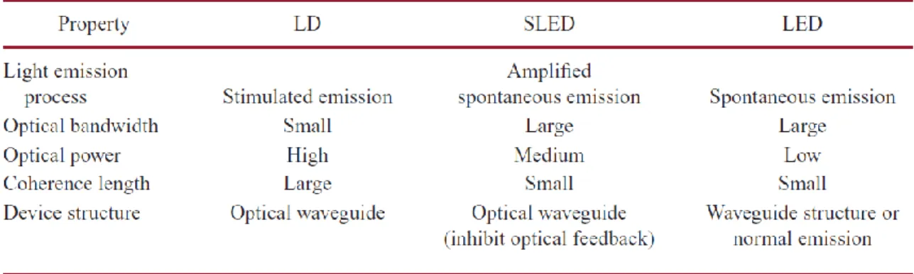
LIST OF TABLES
Table 2.1 Suitability of integration processes for different optical functions [J Van der Tol et al., 2010] ... 13 Table 2.2 Summary of Differences in Operation, Characteristics, and Structures of LDs, SLEDs, and LEDs [Z.Y. Zhang et al., 2010]... 30 Table 2.3 Applications of SLDs [Inphenix, 2011] ... 31 Table 3.1 Comparison of QWI processes regarding the type of heterostructure they are able to process, the final material quality and the final heterostructure quality ... 55 Table 3.2 Comparison of QWI processes regarding their reproducibility, spatial resolution and ease of use ... 55 Table 4.1 PL Peak wavelength as a function of annealing temperature for different irradiation dose (fluence: 155 mJ/cm²) for 4 samples placed on different locations of the support wafer during RTA ... 76
xxi
LIST OF ACRONYMS
Acronym Definition
DFB Distributed feedback
EAM Electro-absorption modulator
Excimer Excited dimer
Exciplex Excited complexes
FWHM Full width at half maximum
GRIN Graded index structure
IBESA Iterative bandgap engineering at
selected areas
ICP Inductively coupled plasma
IID Impurity induced disordering
IFVD Impurity Free Vacancy Disordering
III-V Three-five semiconductor,
semiconductor made of atoms from the third and fifth column of the Mendeleev table
IV Injected current versus the device
bias
Laser – RTA Laser Rapid Thermal Annealing
LD Laser diode
LI Luminescence emission versus the
injected current
MMI Multi-mode interference
MOCVD Metal-organic chemical vapor
deposition
MQW Multi quantum wells
MZI Mach-Zehnder interferometer
Nd:YAG Neodymium-doped yttrium aluminum garnet; Nd:Y3Al5O12
OSA Optical spectrum analyzer
PAID Photo-absorption induced
disordering
PPAID Pulsed photo-absorption induced
disordering
PECVD Plasma enhanced chemical vapour
deposition
PIC Photonic integrated circuit
PL Photoluminescence
PON Passive optical network
QD Quantum dot
QW Quantum well
QWI Quantum well intermixing
RTA Rapid thermal annealing
SGDBR Sampled grating distributing Bragg reflector
SLD Superluminescent diode
SOA Semiconductor Optical Amplifier
UV Ultra-violet
UV-Laser-QWI UV laser induced quantum well intermixing
1
CHAPTER 1
Introduction
Over the last century and a half, the science of light generation has progressed from oil lamp to semiconductor laser and LED emitting over a large range of wavelength and power. After the apparition and democratisation of incandescence light bulbs, fluorescent lamps and laser (initially using ruby crystal [T.H. Maiman, 1960] and Helium-Neon gas [A. Javan et al., 1961] as an active medium), the use of semiconductor crystalline structure has been an incredible step in terms of miniaturization and ease of use of optical systems. Half a century since the first demonstration of semiconductor injection laser [R N Hall et al., 1962; Robert N Hall, 1987], semiconductor light emitting devices (lasers, Light-Emitting Diodes, superluminescent diodes) are today in use everywhere, for everyday lighting, medical imaging, or communication systems. In this last case, fiber optics systems [K.C. Kao, G.A. Hockham, 1966] have consequent advantages over copper line networks, such as data transfer rate increased by several orders of magnitude (Figure 1.1), immunity to magnetic interferences, and increased data transfer security. Nonetheless, numerous progresses and breakthroughs remain to be achieved in the field of photonics, especially in terms of integrated photonic device large scale production. Indeed in a complete optical communication system, a light signal may have to not only be emitted and received, but also modulated, amplified, multiplexed or split. Until recently most of these tasks were accomplished by individual devices interconnected by fiber optics. This generates technical issues such as coupling losses between the different parts and assembling difficulties increasing fabrication cost. To make photonics devices commercially more attractive (for telecommunication, imaging or sensing applications) there appears to be a need to integrate all the aforementioned optical functions on the same chip. This would allow to automatize devices’ fabrication and to reduce their size, thus increasing their reliability, as microelectronics succeeded in doing. With the predicted internet bandwidth requirement explosion (Figure 1.2) and the apparition of sensors using light as part of their detection process, those important developments in the photonics field will be much required in the next decade.
Figure 1.1 Requirements for data transfer and available technologies [G. Lifante, 2003]
In this context, a process allowing the integration on the same wafer of different semiconductor nanostructures suitable for each function required for optical signal processing is a necessity. Indeed, the optimal bandgap profile, refractive index, and absorption may vary depending on the optical function to be performed (for example an active region emitting at a precise wavelength compared to a low absorption passive waveguide). For this purpose, several technologies are in competition and sometimes complementary of one another.
Figure 1.2 Used international bandwidth and projection over the decade [J. Brodkin, 2012]
While purely epitaxial processes based on the growth of a different type of material on different regions of the same wafer allow total control of the different structure parameters, they encounter difficulties in delivering high quality material at an interesting cost. Amongst the competing techniques, post growth quantum well (or dot) intermixing (QWI) structure appears to be among the most versatile, while remaining potentially cost effective. However this process still has to fully demonstrate its reliability and ability to deliver processed structures proper for photonic device fabrication. The content of this thesis is an investigation
of the use of UV laser induced quantum well intermixing (UV-Laser-QWI) process for optoelectronics devices fabrication (namely superluminescent diodes) and the analysis of its abilities in terms of material quality and reproducibility. The use of a laser for QWI brings versatility unattainable via other QWI processes based on ion implantation, inductively coupled plasma or dielectric deposition. Indeed, those processes all require several photo-lithography steps to obtain multiple degrees of intermixing, while laser QWI can pattern a predetermined intermixing map by controlling the laser beam position, shape and dose delivered to the processed wafer.
The following chapter presents an overview of photonics devices physics, from the basis of semiconductor-light interactions to the current photonic integration processes and their applications to optoelectronic devices, with a special focus on the different quantum well intermixing technologies and the superluminescent diodes (their general characteristics and the existing ways to optimize their performances). The third chapter is an exhaustive description of UV-Laser-QWI process, the experimental set up used and the current knowledge on the implied physics. Chapter 4 then provides an analysis of the UV laser based process practicality, with a special attention on the reproducibility, a critical aspect from an industrial point of view. Part of the results were published in an article entitled “Excimer laser induced quantum well intermixing: a reproducibility study of the process for fabrication of photonic integrated devices” in January 2015 [R. Beal et al., 2015]. The benefits of UV Laser QWI for SLD prototyping and the bandgap modifications influence on device performances are analysed in Chapter 5. It contains an article submitted for publication to Optics and Laser Technology and titled “UV laser quantum well intermixing based prototyping of bandgap tuned heterostructures for the fabrication of superluminescent diodes”. Chapter 6 then describes the study of superluminescent emitting device fabrication using IR-Laser-QWI, an alternative to UV-Laser QWI which relies on the joint use of two IR lasers (a 1064 nm emitting Nd:YAG and a 980 nm laser diode) and compares IR-Laser-QWI results and potential with those of UV-Laser-QWI. It contains an article: ‘Enhanced spectrum superluminescent diodes fabricated by infrared laser rapid thermal annealing’ published in December 2013 [R. Beal et al., 2013]. Finally Chapter 7 concludes this manuscript by presenting reflections and comments on potential UV-Laser-QWI applications and leads for
5
CHAPTER 2
Photonics integration state of the art
This chapter presents the background required to fully apprehend optoelectronic devices’ operation and therefore the topic of this thesis. After a general introduction on semiconductor-light interactions, emphasis will be put on photonic integration, its motivations and different technologies, and more specifically on quantum well intermixing. A part of this chapter will be dedicated to a specific device: superluminescent diode, whose fabrication and performance enhancement using UV-Laser-QWI are later studied in this thesis.
2.1 Theory of semiconductor-light interactions
2.1.1 AIII-BV semiconductor band structure and electronic states
The term semiconductor designates a category of material with electrical properties different from insulators and conductors; their electrical conductivity value being between those of these two types of material. Insulators may sometimes be considered as very large band gap semiconductors (see Figure 2.1). Semiconductor band gap energy is in the range of magnitude of kT. Materials with a bandgap over 2 eV are sometimes considered as insulators [B.G. Streetman, S.K. Banerjee, 2000], although this value is arbitrary and strongly depends on the context. For example, gallium nitride (3.4 eV) and aluminium nitride (6.2 eV) are referred to as wide bandgap semiconductors and are used as such in light emitting devices.
Figure 2.1 Occupation states for: (a)(b) Metals, (c) Semiconductor and (d) Insulator (CB: Conduction Band and VB: Valence Band) [C.F. Klingshirn, 2007]
Semiconductors are commonly crystalline solid, although some amorphous materials and liquids can exhibit similar properties. They can be composed of a single pure element (from
column IV of the periodic table) or be a compound (from columns III and V, II and VI, IV and VI, or different group IV elements). For optoelectronics applications, an important distinction has to be made between direct and indirect band gap semiconductors. As shown on energy band diagrams of silicon and indium phosphide in Figure 2.2, direct bandgap semiconductors (like InP and GaAs) have a valence band maximum corresponding to the conduction band minimum when the wave vector k is null. As a consequence, an electronic transition from the conduction band’s lowest energy level to the valence band’s highest energy level is possible without any change of the wave vector value. On the other hand, some semiconductors have a conduction band minimum located at a non-null momentum k value. This means that an electron relaxation implies a change of its momentum (i.e. the emission of a phonon) in addition to an energy loss. The probability of a radiative recombination to occur is consequently much more unlikely than for direct bandgap semiconductor since the radiative recombination time will be longer and therefore most of the recombination will be non-radiative (via a phonon emission at defect locations). Direct gap semiconductors are therefore much more efficient for light generation.
Figure 2.2 Energy band diagrams and major carrier transition processes in indium phosphide (direct bandgap) and silicon (indirect bandgap) crystals [D. Liang, J.E. Bowers, 2010]
Silicon, Germanium and some III/V compounds like GaP and AlAs are indirect bandgap semiconductors. InP, GaAs, GaN and other ternary (AlGaAs, InGaAs) and quaternary (InGaAsP, InAlAsP) compounds are direct bandgap semiconductors commonly used for photonic devices fabrication. Figure 2.3 presents the band gap energies and lattice constants of different III/V semiconductor compounds. Epitaxial growth allows the fabrication of complex nanostructures with atomic layer precision. Thus, the structure composition profile along
growth direction can be tuned to obtain the desired electro-luminescence wavelength and optimize light and carrier confinement. This has to be done, however, with respect of certain conditions of lattice parameter matching.
Figure 2.3 Variation of lattice constant with band gap for the III–V ternary compounds. Solid line: direct gap materials, dashed line: indirect gap material [B. Tabbert, A. Goushcha, 2012]
Three main mechanisms have to be considered in photon / semiconductor interaction in optoelectronics devices, which are described in Figure 2.4. The first is spontaneous emission: an electron loses its energy from conduction band to valence band and emits it as a photon as it moves to a lower energy level. The second is absorption: a photon of given energy excites an electron to a higher energy level. Finally the third mechanism, stimulated emission, occurs when a photon of energy equal to the difference of two energy levels produces a recombination of an electron hole pair. A second photon of equal energy is emitted.
Other semiconductor / light interaction mechanism might have to be considered for device conception, such as non-radiative recombination, Auger recombination, Shockley-Read-Hall recombination.
Figure 2.4 The three electron–photon interactions in semiconductors: (a) spontaneous emission, (b) stimulated absorption, and (c) stimulated emission [S. Kasap, P. Capper, 2007]
2.1.2 Semiconductor heterostructure
Epitaxial processes are capable of a growth thickness precision close to the atomic layer. By growing appropriate adjacent layers of different band gap materials, charge carriers can be confined in a lower gap layer. The electron and hole will then behave like particles in a potential well problem. Instead of having a square root like density of state (DoS) function as for bulk material, electrons DoS presents steps. The better confinement of carriers and the discrete energy steps are advantageous over bulk material for the fabrication of light sources. Figure 2.5 presents different quantum well (QW) structure types used for optoelectronic applications. The separate confinement heterostructure (SCH) improve confinement of the carriers and the optical mode guiding. Graded index SCH (GRINSCH) increases carrier capture efficiency. Finally, the use of staggered multiple quantum wells (MQW) can be used to increase light emission efficiency at high carrier density. Indeed, due to band filling, luminescence saturation can occur for a single quantum well. MQWs structures consequently allow higher light emission power for active devices; however the devices’ threshold gain is also increased.
Figure 2.5 Various geometries of quantum wells active region, (i) single QW(separate confinement heterostructure, SCH), (ii) multiple QWSCH, and (c) GRINSCH (graded-index SCH) structure. (b) Layer
sequence for a separate confinement heterostructure laser [M. Grundmann, J.H. Weaver, 2007]
Other nanostructures can be grown under certain epitaxial conditions, such as quantum wires and quantum dots. While QW are grown in a two dimensional Franck Van Der Merwe mode (one layer after another), with materials of similar or almost lattice constant, self-assembled quantum dots can be grown in Stranski-Krastanov (S-K) mode. QD structures offer several advantages for active device fabrication: a high density of state (lower threshold current for lasers), discrete energy levels (limited emitted wavelength temperature dependence for lasers), symmetric gain function and small active volume (low chirp factor allowing a fast direct modulation).
2.2 AIII-BV semiconductor integration for photonics application
2.2.1 Motivations
As evoked in the introduction, a fully functional photonics integration platform must have the ability to deliver a single device processing several different optical signal operations. To accomplish these tasks, different “building blocks” have to cohabitate on a same chip, blocks similar to the ones described in Figure 2.6, in order to control the direction, intensity and phase of a light signal.
Figure 2.6 The different building pieces that can and need to be integrated on a same chip to provide a complete efficient Photonic Integrated Circuit (PIC) [L.A. Coldren, 2008]
Figure 2.7 presents the evolution of published InP-based PIC complexity until 2010. Since the late nineties, the number of optical functions integrated has been growing exponentially. However, unlike microelectronics, where the transistor is a standard unique unit for counting the number of components implemented on a chip, very different component types coexist in an optoelectronics device. Therefore, in the values indicated in the figure, an active laser, a Mach-Zehnder Interferometer (MZI) or an Arrayed Waveguide Grating (AWG) both count as one component, while they are very different in terms of size and fabrication complexity. If the figure displays only purely InP-based reported photonic integrated circuits, the more recent hybrid integration technology of III/V semiconductor structures on a silicon wafer (presented in the next section) has recently presented a similar exponential growth of their integrated function number, even if it does not yet offer an equivalent integration capacity.
Figure 2.7 Historical trend and timeline for monolithic photonic integration on InP. The vertical scale indicating the number of component is linear, and the red filled circles start at 1 and go to 240. [R. Nagarajan et al., 2010]
2.2.2 Hybrid integration
As already explained, despite silicon being commonly used in microelectronics thanks to its low cost and high purity, its indirect bandgap is a major drawback when it comes to active photonics device applications (even if some photonics components can be made from silicon). Hybrid integration aims to combine silicon and III/V material on the same chip, taking advantage of direct bandgap III/V semiconductor efficiency for light emission and silicon’s price, silicon dioxide passive waveguiding characteristics and compatibility with CMOS technology. Currently, SOI–based optoelectronics components have proven to offer a consequent palette of functionalities: filters, multiplexers, splitters, modulators (using free carrier plasma effect) and photo-detectors [M.J.R. Heck et al., 2013]. However, integration of active light source on silicon has to be realized by adding another gain medium. Since germanium on silicon lasers demonstrate poor performances [J. Liu et al., 2010], processes for obtaining III-V material on silicon have been the subjects of numerous studies. Direct growth of III-V semiconductor on silicon wafer [T. Wang et al., 2011] has a major inconvenience: the
buffer layer which is used to compensate the lattice mismatch is a disturbance for integration. The approach which has offered until now the best results for device fabrication is the wafer bonding of III/V structure on silicon substrate. Several processes are currently being considered: low temperature wafer bonding [A. Black et al., 1997; D. Pasquariello et al., 2000], adhesive bonding [S. Stanković et al., 2011] and silica planarization [B. Ben Bakir et al., 2011]. Different heterostructures have been reported to be bonded on the same Si wafer (for the realisation of a silicon triplexer [H.-H. Chang et al., 2010]).
2.2.3 Monolithic integration
Apart from the indirect/direct bandgap distinction which is crucial for light emitting device design, another important aspect for photonic integration is the necessity of having different heterostructures suitable for all the optical functions required on a PIC. Figure 2.8 illustrates the different solutions that have been used or studied over the past decades for this purpose. These processes are not all suitable for the integration of all devices. The following Table 2.1 presents an evaluation of the different technique suitability for several optoelectronics component integration, as each technique can be more suitable for certain optical functions. The next sections describe the technical aspects of each process and analyze their advantages and flaws.
Figure 2.8 Various techniques for achieving active and passive sections orthogonal to the growth direction [J.W. Raring, L.A. Coldren, 2007]
Table 2.1 Suitability of integration processes for different optical functions [J Van der Tol et al., 2010]
(1) Selective area growth
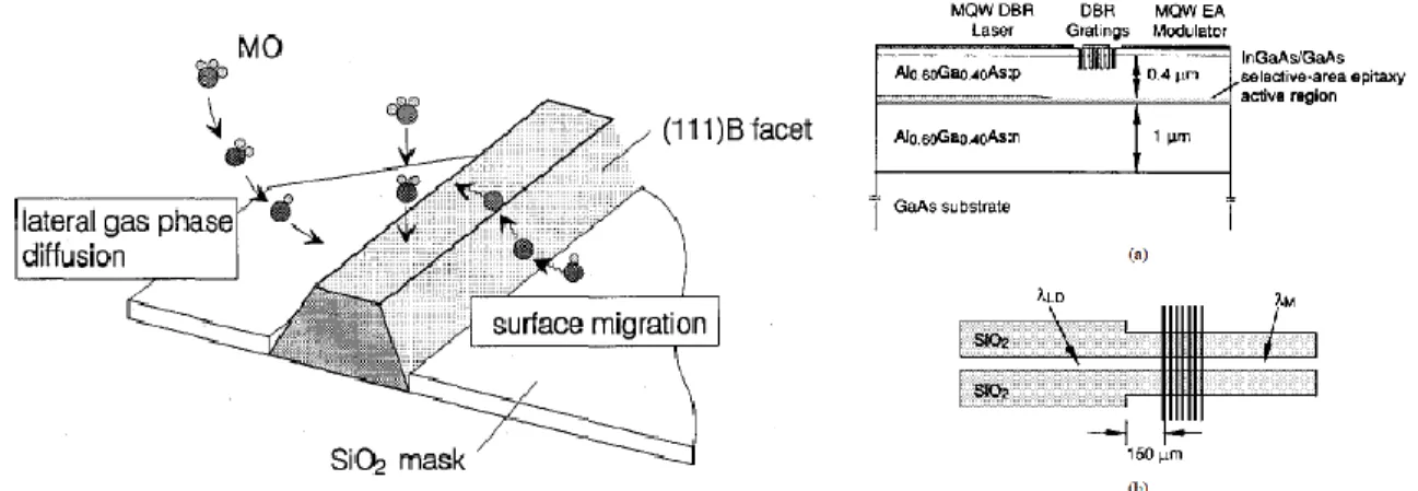
Selective Area Growth (SAG) uses a dielectric mask (usually SiO2) deposition prior to the active region growth [M. Gibbon et al., 1993; T. Sasaki, M. Yamaguchi, 1998]. The mask patterns influence the epitaxial growth rate near them: the epitaxial species unconsumed by the mask migrate to the openings between the dielectric patterns, as depicted in Figure 2.9. Therefore regions between larger mask patterns will grow faster than the others. By using stripes of SiO2 of different widths, it became possible to obtain multiple bandgap wafers in a single growth step as the layer thickness increases with the mask stripe width.
Figure 2.9 Selective area epitaxy process, (a) Schematic diagram of a MQW wavelength-tunable DBR laser with monolithically integrated external cavity EA modulator. (b) Schematic diagram of the dual oxide stripe mask
used during the selective growth of the active region for the device [J.J. Coleman et al., 1997]
Consequently, by adapting the mask, different thicknesses and compositions can be obtained on different regions of the same wafer. However SAG offers only limited flexibility and the control of layer thickness variation in the perpendicular direction can be hard to achieve.
(2) Butt joint regrowth
Butt-joint regrowth is the most versatile of all integration processes. A certain waveguiding structure is grown first and then selectively etched in the regions where it is not required. Finally another structure is grown in those last regions (Figure 2.10), the growth over the first structure being avoided by a dielectric mask. While being the most straight forward process (since it allows the integration of virtually any type of structure) butt-joint regrowth is technically very complex. This complexity is due to the required transition quality between the different structures [A. Talneau et al., 1988; P.J. Williams et al., 1990; C.A. Verschuren et al., 1998]. Indeed those sidewalls are a critical region and any air gap, local variation in composition and growth rate will deteriorate future device performance.
Figure 2.10 Cross-section schematic of a butt-coupled region of integrated amplifier [J. Wallin et al., 1992]
(3) Vertical integration techniques
Due to the practical inconveniences of the two aforementioned epitaxial processes, simpler integration methods were investigated: the growth of two different structures on top of each other on the same wafer. Vertical integration can be divided in two main categories: those implying a regrowth step and those which do not.
- Vertical Twin Waveguide structures / Asymmetric twin waveguide: In the case of twin -guide structures (also designated as Integrated Twin Waveguide (ITG)), two waveguides are grown on top of each other. Also known as vertical evanescent coupling, this concept was developed in the 1970s [R.K. Watts, 1973; Y. Suematsu et al., 1975]. The active layer is grown over the passive one. During device fabrication, the active region is removed where it is not needed (Figure 2.11). While the process is relatively simple from a technical point of view, some difficulties arise due to the interaction of optical modes (odd and even) between the two waveguides. The active section length is therefore a major influence on device characteristics. The addition of a loss layer absorbing the even mode and limiting its interaction with the odd
one only partially solved the problem [L. Xu et al., 1997]. To solve this issue, Asymmetric Twin Waveguide (ATG) structures were introduced, with two waveguides of different confinement. The passive waveguide thickness is larger than the active one, hence the modes’ confinement is different in each waveguide (the odd mode is more confined in the active waveguide and the even mode in the passive one). As a consequence, in the device active region where the two waveguides are coexisting, the odd mode amplification is favoured, its gain being superior and the mode interferences remain limited [P.V. Studenkov et al., 1998; P. V Studenkov et al., 2000]. The main inconvenience of ATG is the need of a taper coupler to transfer efficiently the signal from the active to the passive section. These coupler lengths are typically several hundredths of a micrometer, and occupy an important surface, which is of course not compatible with high density integration.
Figure 2.11 A prospective GaInAsP Integrated Twin Guide laser with three-dimensional output guide [K. Iga et al., 1979]
- Offset / Dual Quantum Well: For both offset and dual quantum wells structures, QWs are grown on top of a waveguiding core and are then selectively removed in the region where they are not needed. The upper cladding of the structure is then added by a regrowth step [M.N. Sysak et al., 2006]. For dual quantum well structures, a second QW region is also grown in the waveguiding core, which does not exist for offset quantum structures. This second QW region allows the integration of EAM using the Quantum Confined Stark Effect with higher modulation bandwidth than for offset quantum well based device (where the EAM is based on the Franz-Keldysh effect). These two approaches proved their efficiency for several applications. However, their capacities are limited to two different structures; therefore high complexity PIC with multi-wavelength light sources cannot be considered. Furthermore,
the regrowth step of the upper cladding adds to the technical complexity of the process, while being less critical than for butt joint regrowth.
(4) Polarisation based Integration Scheme
POLarization based Integration Scheme (POLIS) is an original integration process compared to every other one in that it does not rely on the integration of several bandgap structures (either in the horizontal or vertical direction) [U. Khalique et al., 2007]. POLIS is based on the different behaviour of a light signal depending on its polarization. The devices here are made from a strained quantum well structure. This separates the heavy-hole (associated with TE-transitions) and light-hole (mostly associated with TM-TE-transitions) valence band energies: compressive strain increases the heavy-hole energy level and decreases the light-hole one. Consequently, at the same wavelength, a certain polarization will be absorbed by and not the other [Jos van der Tol et al., 2006]. By adding polarization converters, it is possible to change the light signal polarization to make active / passive waveguide sections from the same material. Therefore POLIS requires the integration of efficient low loss polarisation converters [D.O. Dzibrou et al., 2013]. While interesting for some devices [U. Khalique et al., 2002; A.J.G.M. Van De Hulsbeek et al., 2006], POLIS remains limited by its technical imperatives: polarization converters are required between each active and passive sections (although they can be only 125 µm long) and the obligation to use a certain type of heterostructure.
As we have seen, all the aforementioned techniques have major drawbacks such as epitaxial complexity increasing fabrication costs or conception imperatives limiting devices’ design and performances. Quantum Well Intermixing (QWI), the integration process category studied and used in this work, is a post growth process aiming to provide cost effective multi bandgap structures for photonic integration [J.H. Marsh, 1993].
2.3 Quantum well intermixing
QWI is based on the crossed diffusion of species between well and barrier. This atomic composition variation changes the well energy levels, and consequently, the forbidden band gap energy. The barrier / well intermixing results in an increase of the well bandgap energy (Figure 2.12), thus the intermixing effect is usually referred to as a “blue shift”, since the emission wavelength decreases (and gets closer to the blue). Since QWI aims to modify selectively certain regions of the wafer, the control of the intermixing rate between barrier and
well species and the spatial definition are the two major parameters that the differently developed QWI processes are aiming to optimize.
Figure 2.12 Illustration of the intermixing process for a GaAs/AlGaAs quantum well: on the left the QW prior to intermixing, on the right after intermixing, some Aluminium has mixed into the QW and increased its gap energy
[Intense, 2013]
The rest of this section presents the process physics and a review of the different ways to achieve QWI that have been published.
2.3.1 General principles
Intermixing of barrier and well species can be achieved by annealing the heterostructure at a sufficient temperature (typically close to 900°C for GaAs/AlGaAs QWs and 700°C for InGaAs/InGaAsP QWs). However this would blue shift the entire wafer, which is not compatible with multi bandgap wafer production. To modify locally QW bandgap, the wafer can either be annealed locally using a wafer or point defects can be introduced locally into the wafer. Point defects thermal stability is lower than that of the heterostructure, which means they will diffuse at annealing temperatures lower than the heterostructure limit. By controlling the amount of point defects created and their diffusion, the QW blue shift can be controlled too. Most QWI processes rely on the thermally induced diffusion of point defects (namely interstitials or vacancies), whose different mechanisms are described in Figure 2.13.
Figure 2.13 Schematic illustration of diffusion mechanisms. (a)Top: exchange mechanism, bottom: ring mechanism. (b) Vacancy mechanism. (c) Interstitial mechanism. (d) Interstitialcy mechanism. (e)
Substitutional-interstitial mechanisms, top: Frank-Turnbull mechanism, bottom: kick-out mechanism [U.W. Pohl, 2013]
Theoretical models have been developed to describe intermixing in quantum well structures. The models may differ depending on the heterostructure type. The simplest models are those describing intermixing in structures combining a binary and a ternary compound, such as is for GaAs/AlGaAs [T.E. Schlesinger, T. Kuech, 1986] or InGaAs/GaAs [W.P. Gillin et al., 1993] systems. Hence, only group III species diffusion is considered since there is no concentration gradient for group V atoms (arsenic). The Group III atom diffusion in the crystal growth direction is commonly described by using Fick’s second law:
𝜕𝐶 𝜕𝑡 = 𝐷
𝜕2𝐶
𝜕𝑧2 (2.1)
In this equation, C is the species concentration and D it diffusion coefficient. In this situation, group III species diffusion coefficient is considered equal for all. The group III species diffusion length Ld quantifies the intermixing process:
𝐿𝑑 = √𝐷𝑡 (2.2)
For structures that implied a binary and a ternary compound, like GaAs/AlGaAs or InGaAs/ GaAs systems, only group III element diffusion has to be considered. For a GaAs/AlGaAs QW, where aluminium atoms are initially only in the barriers, the aluminium concentration profile can be described as[J. Crank, 1979]:
𝑤̃𝐴𝑙(𝑧) = 𝑤𝐴𝑙{1 −1 2[𝑒𝑟𝑓 ( 𝐿𝑧+ 2𝑧 4𝐿𝑑 ) + 𝑒𝑟𝑓 ( 𝐿𝑧− 2𝑧 4𝐿𝑑 )]} (2.3)
And in the case of an InGaAs/GaAs well, where indium is initially only present in the well and absent in the barriers:
𝑤̃𝐼𝑛(𝑧) =𝑤𝐼𝑛 2 {[𝑒𝑟𝑓 ( 𝐿𝑧+ 2𝑧 4𝐿𝑑 ) + 𝑒𝑟𝑓 ( 𝐿𝑧− 2𝑧 4𝐿𝑑 )]} (2.4)
wAl and wIn being the initial Al and In molar fractions in the barriers and well respectively, Lz the well thickness, z the position in the heterostructure and erf the error function. This model has been experimentally confirmed. However it is not valid anymore for the InGaAs/InP system or other quaternary compound made quantum wells. [K. Mukai et al., 1994] developed a detailed model of intermixing of group V atoms in an InGaAsP system. In this model, group V atoms diffuse at different rate in the well and in the barriers. The diffusion is described using a linear equation:
𝜕𝐶𝑖(𝑧, 𝑡) 𝜕𝑡 = 𝐷𝑖
𝜕2𝐶 𝑖(𝑧, 𝑡)
𝜕𝑧2 (2.5)
Where i = b for barrier and i = p when the well is considered. The discontinuity at the interface and the diffusion flux continuity gives:
𝐶𝑏(𝑧, 𝑡) = 𝑘𝐶𝑝(𝑧, 𝑡); z L (2.6)
And
𝐷𝑝𝜕𝐶𝑝𝜕𝑧(𝑧,𝑡)= 𝐷𝑏𝜕𝐶𝑏𝜕𝑧(𝑧,𝑡); z L (2.7)
k is the concentration ratio at the well/barrier interface. [K. Mukai et al., 1994] then compares his model to PL measurement for AlGaAs and InGaAsP well, obtaining empirical data for the k factor.
2.3.2 Impurity induced disordering
The very first quantum well intermixing phenomenon to be studied, more than 30 years ago [W.D. Laidig et al., 1981], relied on the diffusion of zinc impurities introduced in the heterostructure (by annealing the material). Although the first observed, this technique has the important inconvenience of modifying the doping of the heterostructure, and is consequently by far not the most suitable technique for optoelectronics device fabrication. It is, however, a relatively simple and accessible way to induce intermixing for academic study concerning layer disordering [T. Lin et al., 2013]. To locally introduce the impurities, ion implantation layer disordering has been developed. Focused Ion Beam (FIB) may be used for such a purpose [J.P. Reithmaier, A. Forchel, 1998], however FIB is not efficient to process large sample surface, and ion implanters are more suitable. Ion implantation is a well-developed


![Figure 3.17 Comparison of as-grown and intermixed laser diode LI characteristics [Jonathan Genest, 2008]](https://thumb-eu.123doks.com/thumbv2/123doknet/3424514.99975/82.918.238.631.131.446/figure-comparison-grown-intermixed-laser-characteristics-jonathan-genest.webp)