HAL Id: hal-03244613
https://hal.archives-ouvertes.fr/hal-03244613
Submitted on 1 Jun 2021HAL is a multi-disciplinary open access
archive for the deposit and dissemination of sci-entific research documents, whether they are pub-lished or not. The documents may come from teaching and research institutions in France or abroad, or from public or private research centers.
L’archive ouverte pluridisciplinaire HAL, est destinée au dépôt et à la diffusion de documents scientifiques de niveau recherche, publiés ou non, émanant des établissements d’enseignement et de recherche français ou étrangers, des laboratoires publics ou privés.
Photoluminescence probing surface passivation of highly
doped ntype InP samples
Wei Zhao, Baptiste Bérenguier, Cendra Rakotoarimanana, Anne-Marie
Goncalves, Arnaud Etcheberry, Mathieu Frégnaux, L Lombez, Jean-François
Guillemoles
To cite this version:
Wei Zhao, Baptiste Bérenguier, Cendra Rakotoarimanana, Anne-Marie Goncalves, Arnaud Etcheberry, et al.. Coupled Time Resolved and High Frequency Modulated Photoluminescence prob-ing surface passivation of highly doped ntype InP samples. Journal of Applied Physics, American Institute of Physics, In press. �hal-03244613�
Coupled Time Resolved and High Frequency Modulated
Photoluminescence probing surface passivation of highly doped
n-type InP samples
Wei Zhao (1), Baptiste Bérenguier (2), Cendra Rakotoarimanana (3), Anne Marie Goncalves (3), Arnaud Etcheberry (3), Mathieu Frégnaux (3), Laurent Lombez (2), Jean-François Guillemoles (2),
1) Institut Photovoltaïque d'Ile de France, 91120 Palaiseau France
2) UMR IPVF 9006, CNRS, Ecole Polytechnique Institut Polytechnique de Paris, PSL Chimie ParisTech, IPVF SAS, 91120 PALAISEAU, France
3) ILV - Institut Lavoisier de Versailles UMR 8180 CNRS/UVSQ, Saint-Quentin-en-Yvelines
Abstract
Electronic passivation of III-V surfaces is essential for applications in optoelectronic devices. A key aspect is the measurement of the surface recombination properties which can be done by various techniques including transient photoluminescence (TRPL) or luminescence quantum yield. These measurement techniques are always indirect since they suppose postulating a mathematical model for the data interpretation. Most common models use the notion of surface recombination velocity to quantify the surface recombination. In this paper we demonstrate on InP substrate than this notion is not always sufficient to represent the injection dependence of the surface phenomena. The study of power dependence of TRPL decays coupled with Modulated Photoluminescence (MPL) spectra on four samples from the same wafer with different surface treatments (epi-ready, freshly cleaned, after air exposure and with poly-phosphazen passivation) allows us for discriminating between bulk and surface properties. We introduce surface defect trapping as an alternative to explain TRPL decays and MPL phase excitation power dependences of the three non-passivated samples. Surface trap parameters such as capture cross section and defect density are extracted. The passivated sample exhibits invariant response shape on eight orders of magnitude of illumination. The stability of the PL response at high flux is in agreement with the perfect stability of the passivation layer which is able to protect the InP surface without chemical changes over more than one year. They are linked to the nature of the Passivation layer/InP interface. Other surface treatments were found to have an injection dependent response
After it is published, it will be found at https://aip.scitation.org/journal/jap or https://doi.org/10.1063/5.0033122
at high flux corresponding to different surface defects distribution but also possibly to surface chemical changes for the freshly cleaned sample.
INTRODUCTION
III-V semiconductors are recognized as high-performance materials for the fabrication of (opto)electronic devices such as avalanche photodiodes, light emitting diodes and lasers. For many years, Indium Phosphide (InP) based thin film III-V emitters (GaxIn1-xP and GaxIn1-xAsyP1-y) have
been commonly used by the optoelectronics industries 1 and are top candidates for Photonic
Integrated Components 2. However, the surface and interface properties of these materials can
degrade the overall performances of the layers/devices. To address this, numerous chemical treatments have been developed to improve the surface properties of InP, and first of all surface chemical and electronic passivation 3–5. In parallel, advanced contactless optical characterization
methods have proved to be powerful to determine carriers’ dynamics and recombination mechanisms in semiconductor materials. A standard method, Time Resolved Photoluminescence (TRPL), has been used for probing sub nanosecond recombination mechanisms. Nevertheless, the interpretation of the TRPL temporal decays may be difficult when presenting non mono-exponential behaviour 6. Generally, determination of the surface/interface recombination
mechanisms is not a simple task since there is no straightforward contactless characterization technique to measure the surface state density and other physical properties with sufficient accuracy. The main difficulty lies in the dissociation of the relative contribution of bulk and surface from the raw TRPL decays. The surface recombination velocity (SRV) can affect the TRPL decay times by causing surface depletion (or accumulation) of excess carriers and competing with bulk recombination and surface band bending 7,8. The SRV in InP is supposed to increase with the
doping density until it is limited by the thermal velocity of carriers. In one early study, Bothra et al. 9 found that an increase of doping from 3×1015 cm-3 to 3×1018 cm-3 caused an increase of SRV
from 5000 cm/s to 1×106 cm/s. Other benchmarking studies using in situ photoluminescence (PL)
quantum yield measurements or time resolved photo-gratings investigate InP surface states (attractive traps) and found fixed positions of the Fermi level at the surface and constant SRV for various doping densities of InP as well as several treatments of the surface 10–12. Improvement of
(DIGS) of Hasegawa postulating U-shape density of interface states 13–15 . Pinning of the Fermi
level at about 1 eV above the valence band maximum was observed in both highly doped (1018 cm -3) n and p type (100) InP surface despite the surface treatments. Rosenwarks et al. also studied
TRPL decays on one highly n doped sample but without mentioning SRV 16. The authors concluded
that the non-radiative recombination and the effective lifetime are insensitive to the injection level. Moreover, for undoped InP, the radiative coefficient is found to be 2×10-11 cm3/s, which is the
lowest value reported. The question of the value of this coefficient for high doping remain open. In order to provide complementary information, another approach, called Modulated Photoluminescence (MPL) or Frequency Domain Photoluminescence, can also be used to investigate carrier lifetime in semiconductors. By using sinusoidal illumination variation and recording the phase shift between the excitation signal and emitted signal, one can assess the carrier lifetime for example in silicon wafers 17. Extended to the MHz range, the High-Frequency MPL
(HF-MPL) can probe short lifetime and be closer to the real excitation conditions (i.e. close to continuous wave excitation by tuning the modulation amplitude). It also enables focusing on mechanisms that usually appear in the noisy end of the decay such as the carrier detrapping 18.
Great efforts have already been done previously on silicon and CIGS samples 18–20. Reklaitis et al.
also highlighted this frequency-domain photoluminescence technique in their study of carrier lifetime in InGaN light-emitting diode and proposed Fourier transform of TRPL decay models to fit the data 21,22. Pulsed and modulated excitation can thus be compared if the solution for the
sinusoidal excitation is derived from impulse response i.e, when the underlying mathematical equation system is linear. The proven advantage of Frequency Domain techniques is that they can investigate several orders of injection level below TRPL 22.
We here adopted the approach of combined TRPL and MPL techniques to probe four highly n-type doped InP from the same wafer with different surface treatments (epi-ready, freshly cleaned, after air exposure and with poly-phosphazen passivation). Such poly-phosphazen layers have proven to protect chemically the surface since no oxidation of the initial clean surface was observed over more than 1 year 23–25. Detailed XPS analysis can be found in Gonçalves et al 26. , It is yet to be
investigated how they passivate the surface electronically and behave at high illumination flux. The modulation frequency range of our HF-MPL setup has been extended to 200 MHz to investigate fast carriers’ dynamics while keeping high sensitivity detection, similarly to TRPL techniques. The
fittings on the experimental data of both TRPL and MPL experiments were performed by using a drift diffusion simulator developed in our institute to investigate the surface recombination mechanism 19. Two other strong points of our approach are: i) The simultaneous fit of data acquired
from the two technics and for different illumination levels; ii) the correction of the MPL and TRPL data with respects to the system optical transmission rather than a normalization to unity. These two features strongly reduce the risk of finding an unphysical solution when fitting the data with numerous parameters. This parallel experimental and modelling approach goes beyond a simple TRPL data analysis, it evidences a quantitative SRV measurement as well as the determination of minority carrier lifetime, defect density, capture cross section for both electrons and holes and defect levels 27. It is a continuation of the methodology of Hasegawa’s group extending it to time
resolved technics. In the next section we describe the samples and the methodology, then the results will be presented and discussed.
METHOD
1.Sample description
The InP 350 µm thick samples are Sn doped with an n-type doping level was measured by Mott-Schottky method to be around 3×1018 cm-3. The four samples are studied coming from the
same wafer with different surface treatments presented in the Table 1. Poly-phosphazen layer was deposited on “PH” sample in liquid ammonia to form a very thin film which has been characterised by XPS experiment. XPS data for the film are inserted in supplementary material showing the strong uniformity and small thickness of the film. The charge current monitoring during the deposition process gives a one monolayer of phosphazen formation which is consistent with XPS data. 26. “Epi” sample (epi-ready wafer), was left untreated from supplier. “Desox” has been
cleaned by 2 M HCl solution before the measurement in order to eliminate the oxide layer. After two weeks in ambient atmosphere, we measured “Desox” again as “Reox”
Table 1 Samples’ basic information for experimental measurements and simulations28
Sample Epi Desox Reox PH
HCl surface cleaning (2 M) No Yes (2weeks in Yes air after)
No
Poly-phosphazen layer No No No Yes
Doping density (cm-3) 3×10¹⁸ 350 1.30 12.5 4.38 720 80 3.9×10⁷ 1.7×10⁷ 5.7×10¹⁷ 1.1×10¹⁹ Thickness (μm) Bandgap, Eg (eV) Relative permittivity, ɛr
Electron affinity (eV) Electron mobility, μn (cm2V-1s-1)
Hole mobility, μp (cm2V-1s-1) Electron thermal velocity, νn ( cm.s-1)
Hole thermal velocity, νp ( cm.s-1)
Conduction and Valence band density of states, Nc, Nv (cm-3)
2.Measurement principle
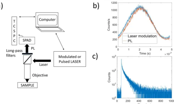
Figure 1 (a) Sketch of the MPL/TRPL experimental setup. The setup is a conventional microscope using long pass filters for separating the laser light and the photoluminescence; (b) Modulated signals: direct measurement of the laser light (blue) when removing the long pass filters, PL signal of an InP wafer sample (red) presenting a phase shift (delay) with respects to the laser light modulation; (c) Typical TRPL decay.
The setup is sketched in Figure 1. The light sources are a 638 nm wavelength intensity modulated laser and a 532 nm pulsed laser with 80 ps pulse duration at 5 MHz repetition rate. The modulation is based on sinusoidal variations of the light intensity around a given working point. In this study the ratio between modulated and continuous part of the modulated light is close to 60%. Samples are excited with a beam diameter of 50 μm: it ensures an excitation spot larger than the diffusion length avoiding lateral transport of the photogenerated carriers which might influence the carrier dynamics. To detect the PL signal with an optimal sensitivity we used a Single Photon Avalanche Detector. Then, the Picoharp 300 Time Correlated Single Photon Counter (TCSPC) and the in house LabVIEW code allow reconstructing one decay in TRPL mode or one period of the modulated signal. In such configuration we obtain a unique experimental setup to record fast modulated signal with a high detection sensitivity, contrary to usual modulated experiments where the sensitivity is strongly degraded because of the use of fast detector (compromise between speed and gain). Once the modulated signal is recorded, we can extract the phase and amplitude of the first harmonic by fast Fourier transform. Finally, we record the phase and the amplitude of the first harmonic at each frequency and we calculate the phase shift between the laser and photoluminescence.
3.Simulation procedure
The fitting procedure was performed by using a in house LabVIEW simulator based on drift-diffusion equations, the Shockley Read Hall (SRH) recombination model and optical models
19. The fits were made using a least square minimization procedure with normalized error (see
Supplementary Materials). The absorption coefficient was measured and taken into account (see Supplementary Material). Details of the simulation are given just below. Please note that for each sample, the fit was performed simultaneously to all the TRPL decays and the MPL real and imaginary parts leading to a unique set of parameters. Furthermore, the TRPL and MPL maximal intensities were not normalized to unity as in usual procedures. At high laser fluence, we used neutral densities to avoid detector saturation by the emitted PL. We measured the attenuation of the densities at the PL wavelength and corrected the data by dividing by these attenuation factors.
The experimental data were obtained under several illumination flux and fluences. We note that the samples are illuminated until a steady transient emission is achieved. The MPL phase and amplitude spectra were depicted by Fourier transform for modulated frequency ranging from 50 kHz to 200 MHz and fluxes varying from 5×10¹⁴ to 3×10²¹ photons.cm-2s-1 (equivalent for about
0.005 sun to 30 000 sun). The TRPL decays were recorded at the same sample location by different excitation powers with illumination fluences from 7×10⁶ photons.pulse-1.cm-2 to 9×10¹³
photons.pulse-1.cm-2
.
3.1 Bulk Simulation
The one-dimensional transport of electrons and holes in a semiconductor material can be efficiently represented by the drift-diffusion system (equations 1-4) coupled to a Poisson equation (5). With the electron and hole densities (n, p), the respective currents (Jn,p), and the diffusion coefficients (Dn,p) and mobilities (µn,p), the optical generation rate (G), the recombination rate
(Rrec), the electric field (F) and the doping level (Cdop), the equation system reads:
𝜕𝑛 𝜕𝑡 = 1 𝑞𝑑𝑖𝑣 (𝐽 ) + 𝐺 − 𝑅 (1) 𝜕𝑝 𝜕𝑡 = − 1 𝑞𝑑𝑖𝑣 𝐽 + 𝐺 − 𝑅 (2) 𝐽 = 𝐷 𝑔𝑟𝑎𝑑(𝑛) + 𝜇 𝑛𝐹 (3) 𝐽 = 𝐷 𝑔𝑟𝑎𝑑(𝑝) − 𝜇 𝑝𝐹 (4) 𝑑𝑖𝑣(𝐹) =𝑞 𝜀 𝑝 − 𝑛 + 𝐶 (5)
The two first equations express the charge conservation as a function of the currents, the generation, the recombination. The currents of electrons and holes are separated and associated to diffusion and drift terms (3-4). The Poisson equation completes the system (5). The one-dimensional drift diffusion simulation code allows us to reproduce the HF-MPL/TRPL data at the same time with the same parameters. The code uses a 1D spatial discretization of the drift diffusion equations as presented in 29,30 in combination with Differential Algebraic Equations solvers (DAEs)
for the temporal part. MATLAB ODE15s was used but IDAS 31 can also be used with similar
results. This approach has been proved to be efficient 32. The code includes the following
recombination mechanisms: radiative, Auger, SRH1. The outputs provide the carriers densities
profiles n and p as well as the electric potential for a given semiconductor stack with respect to depth and time. Light excitation G(t,x) can follow arbitrary time profiles, such as short impulsion (TRPL) or sinusoidal variations (MPL).
Since the doping level is high (3×1018 cm-3) for all samples, and the injection level during TRPL
never reaches the doping level for these samples, we chose to represent the recombination in the bulk by a single lifetime τb. Then with ni being the intrinsic concentration,
𝑅 =𝑛𝑝 − 𝑛
𝑛 𝜏 (6)
The boundary condition at the backside involves local electro neutrality, which is a good assumption since the photo generated carriers do not reach the back side. At the front side, we use the SRH formalism for the boundary conditions.
1 SRH can use the stationary or time dependent form, i.e rate equations. In the second case a supplementary equation
3.2 Shockley Read Hall surface time dependent recombination
The recombination at silicon surface was already successfully represented by Aberle 33 using
SRH formalism in stationary regime. Rosenwaks also took into account the surface charge created by the difference of capture rates for electrons and holes at the surface in time dependent experiments 34. A common approximation in the literature is to use stationary SRH formula even
in the case of transient experiments, but it. can lead to erroneous results, so it was not used. by representing the recombination at the surface or at the InP surface or at the InP/poly-phosphazen interface by a time dependent SRH mechanism. It involves a continuous energetic distribution of traps at its surface. For each energy level of the distribution, assuming that the density of traps per surface unit and per energy unit is NT(E) and the corresponding number of trapped electrons nT(E),
the emission and capture rates of the surface levels lying inside the bandgap for both type of carriers are classically expressed in Shockley Read Hall theory as follow 35:
𝐸𝑚𝑖𝑠𝑠𝑖𝑜𝑛 = 𝜎 𝑣 𝑛∗𝑛 (𝐸) (7) 𝐶𝑎𝑝𝑡𝑢𝑟𝑒 = 𝜎 𝑣 𝑛 𝑁 (𝐸) − 𝑛 (𝐸) (8) 𝐸𝑚𝑖𝑠𝑠𝑖𝑜𝑛 = 𝜎 𝑣 𝑝∗ 𝑁 (𝐸) − 𝑛 (𝐸) (9) 𝐶𝑎𝑝𝑡𝑢𝑟𝑒 = 𝜎 𝑣 𝑝𝑛 (10)
Here σn,p stands for the capture cross sections of the defects for electrons and holes, respectively,
νn,p stands for the thermal velocities for electrons and holes, respectively, Nt(E) is the trap density
per surface unit are and nt is the density of trapped electrons per surface unit.
These emission and capture rates represent the capture and emission rate (cm-3.s-1) for electrons of
the conduction band at the surface ((7) and (8)) and for holes from the valence band ((9) and (10)) for each energetic level present in the surface density of states. One can note that the capture rates involve bimolecular processes (n*(Nt-nt) product or p*nt product) where the emission rates are monomolecular and involve n* and p* quantities. The quantities p* and n* are related to the
conduction and valence band equivalent densities of states Nc, Nv and the corresponding band gap edges Ec, Ev:
𝑛∗ = 𝑁 exp −𝐸𝑐 − 𝐸
𝑘𝑇 (11)
𝑝∗ = 𝑁 exp −𝐸 − 𝐸𝑣
𝑘𝑇 (12)
And the system is determined by the set of time dependent equations: At each E, 𝜕𝑛 (𝐸) 𝜕𝑡 = 𝐶𝑎𝑝𝑡𝑢𝑟𝑒 − 𝐸𝑚𝑖𝑠𝑠𝑖𝑜𝑛 + 𝐸𝑚𝑖𝑠𝑠𝑖𝑜𝑛 − 𝐶𝑎𝑝𝑡𝑢𝑟𝑒 (13) 𝜕𝐽 𝜕𝐸 = −𝑞(𝐶𝑎𝑝𝑡𝑢𝑟𝑒 − 𝐸𝑚𝑖𝑠𝑠𝑖𝑜𝑛 ) (14) 𝜕𝐽 𝜕𝐸 = 𝑞 𝐶𝑎𝑝𝑡𝑢𝑟𝑒 − 𝐸𝑚𝑖𝑠𝑠𝑖𝑜𝑛 (15)
Finally, the total charge at the surface for donor-like and acceptor-like traps as well as the total electrons and holes currents will be, with q the positive elementary charge:
𝑄 = −𝑞 𝑛 (𝐸)𝑑𝐸 (16)
𝑄 = 𝑞 (𝑁 ( )− 𝑛 (𝐸))𝑑𝐸 (17)
𝐽 = 𝜕𝐽
𝐽 = 𝜕𝐽
𝜕𝐸 𝑑𝐸 (19)
The electric field at the surface will follow:
𝜀𝐹 = 𝐶ℎ𝑎𝑟𝑔𝑒 (20)
The above formula represents the currents and the charge changes for donor or acceptor defects at the surface. In the case of stationary regime, we get the following currents and charge at the surface 33. 𝐽 = 𝐽 = 𝑞 𝑛 + 𝑛𝑛 𝑝 − 𝑛 ∗ 𝑆 + 𝑝 + 𝑝∗ 𝑆 𝑑𝐸 (21) 𝑄 = 𝑞 𝑁 𝜎 𝑛 + 𝜎 𝑝 ∗ 𝜎 (𝑛 + 𝑛∗) + 𝜎 (𝑝 + 𝑝∗)𝑑𝐸 (22) 𝑄 = 𝑞 𝑁 𝜎 𝑛 ∗+ 𝜎 𝑝 𝜎 (𝑛 + 𝑛∗) + 𝜎 (𝑝 + 𝑝∗)𝑑𝐸 (23)
Sn and Sp are so called surface recombination velocities and are given by
𝑆 = 𝑁 𝜎 𝑣 (24)
𝑆 = 𝑁 𝜎 𝑣 (25)
The analysis made in this work will be performed with a single level and with the time dependent equations but the values of the stationary SRV will be given for comparison with literature.
RESULTS AND DISCUSSION
Using the simplest model where only the bulk lifetime of minority carriers and minority carrier SRV were simulated as fitting parameters. The fitting results were not satisfactory because using a single SRV is not sufficient to reproduce the injection dependence of the signal. For similar samples (see Supplementary Material) simulation gave an excessively long bulk lifetime of 42 ns, higher than the lifetime of radiative recombination which is 15 ns (maximum value calculated from the literature : krad rangesfrom 2×10-11 to 1.2×10⁻¹⁰ cm3.s-136,37).
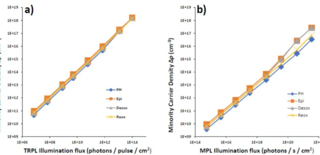
We therefore had to upgrade the model up to a sufficient complexity with five parameters including minority carrier lifetime in bulk (τbulk), defect density (Nt), capture cross section for both electrons (σn) and holes (σp) and defect level (Et). Note that we choose to introduce one single level instead of a continuous distribution. It assumes that the surface recombination rates can be represented by with only four parameters. We will discuss the validity of this assumption later. Fitting parameters are summarized in table 2. A range is given rather corresponding to the 95% confidence interval (except for the surface recombination velocities extracted from the fit). Once the fitting parameters were extracted, the maximal excess carrier density for each illumination flux has been calculated by equations (1)-(20) and plotted in Figure 2. According to our solver, the hole quasi-Fermi level position is found at 1.27 eV from conduction band for TRPL and 1.22 eV for MPL at the maximum illumination, meaning that the surface defect system is scanned nearly all over the bandgap (see band diagram in the Supplementary Material).
It can be observed that the maximal excess carrier densities are linearly dependent with the illumination fluences for at low illumination and deviate slightly at high fluences. However, the injection level remains below the doping level.
Theoretically, the comparison of the MPL experimental and calculated average intensity at high illumination fluxes could allow to perform the Photoluminescence Surface State Spectroscopy method 14,15. Unfortunately, at such high doping level it would require more than 1022 photons.cm -2.s-1 and it would become difficult to prevent sample heating and Auger recombination.
For all samples, the bulk lifetime was determined to be in the range 10-13 ns. Regarding the high doping level, it implies that the radiative constant is in the same order of magnitude than the one found by Liu and Rosenwaks 16 which report the lowest value in the literature (2x10-11 cm -3.s-1). Any larger value would shorten the decays and reduce the MPL phase.
Figure 2 Simulated maximal injection level presented by excess carrier density vs illumination power for a) TRPL and b) MPL for the four samples
Table 2 Detailed fitting results for conjugated MPL/TRPL simultaneous fitting with surface defect on the four samples
Fitting Parameters PH Epi Desox Reox
Bulk lifetime, τbulk (ns) 12 (10-13)
Defect density, Nt (1010 cm-2) 20 (3-100) 4 (2-8) 60 (40-80) 360 (300-600) Electron capture
cross-section, σn (cm2) 2×10-16 (4-100 ×10-17 ) 1×10-17 (0.7-2×10-17) 5×10-19 (4-8×10-19) 4×10-17 (2-6×10-17)
Hole capture cross-section, σp (cm2) 4×10-13 (1-18×10-13) 8×10-14 4-15×10-14 1×10-14 (0.8-2×10-14) 6×10-16 (0.3-1×10-15)
2.Sample comparison
The data of the PH sample are presented in figure 3 for different excitation intensities. Other data are presented in the Supplementary Material. The specificity of the PH sample is that the temporal response remains similar over eight orders of magnitude (except the background at low intensity curves). This is due in part to slightly larger capture cross sections for both electrons and holes of the defects system in compare to the three other samples. This enhances surface recombination and prevents surface trap saturation. For such highly doped samples, the surface has a higher recombination rate than the other samples and the poly-phosphazen is not found to reduce the surface recombination.
All the other samples present an injection dependence on both the MPL and the TRPL signature. This dependence is mainly due to the asymmetric capture cross sections, the postulated trap center being not able to capture enough electrons at high fluences. The fits were however not completely satisfactory at really high fluence (two last TRPL decays). This can be due to measurement uncertainty, but also to the appearance of another mechanism such like radiative or Auger recombination. We can also note that the fit of the MPL phase is unsatisfactory for “Desox”, while the amplitude and the TRPL decays are well fitted. Indeed, it raised a question about the chemical stability of ‘Desox’ surface during the experiment. As the holes are strong reducing species, a photo induced re-oxygenation of the surface at strong illumination fluxes may be an explanation for this behaviour.
In comparison to references 14,38, we found similar magnitude for the hole capture cross sections
when our electron capture cross section are smaller by several order of magnitude. We found these capture cross sections to be sample dependent. As different capture cross sections would strongly change the PL intensity dependence to illumination fluxes and fluences for either MPL or TRPL
Surface Recombination Velocity, Sn = Ntσnνn (cm.s-1) 2 x10 3 24 12 6 x10³ Surface Recombination Velocity, Sp = Ntσpνp (cm.s-1) 1 x10⁶ 5 x10⁴ 1 x10⁵ 4.5 x10³
or both, we conclude that the samples surface are different from 38. The calculated minority carrier
SRV are also in the agreement with those reported in the literature, where for the doping density from 3×1015 cm-3 to 3×1018 cm-3 caused an increase of SRV from 5000 cm/s to 1×106 cm/s 9. Note
we also provided the majority carrier SRV which allows for a real simulation of the surface.
Figure 3 Conjugated MPL/TRPL simultaneous fitting with surface defect on PH sample. MPL phase (a), amplitude (b). Experimental data are in symbols and fitting curves are in line; TRPL
decays (c) and fits. Detailed fitting results are presented in Table 2.
3.Discussions about the oxide charge, and the surface density of state.
Surface photovoltage experiments (SPV) were performed indicating no significant band bending at the samples surface for PH, ‘Reox’ and ‘Epi’ sample. According to our simulations, an additional charge superior to 1012 elementary charges per cm-2 is necessary to modify the TRPL
and MPL response. Indeed, our fitting procedure always converged to fixed charges inferior to this value. A higher charge was found to be incompatible with the observed injection dependence of the data
In the present article we chose to represent the surface density of state by a single level. This could correspond to three different cases. First case involves a real single level at the surface due for example to an impurity (most probably the case of the sample “EG1” presented in Supplementary Material). In the second case the surface density of states (DOS) is dominated by deep centers. In this case the reemission terms are negligible due to the smallness of n* and p* and the postulated single level represent the total density of state of these levels, as the full distribution is not experimentally accessible. In the third case, which is the most probable, the model is correctly simulating a complex density of state at the surface.
We also simulated a U-shaped density of states for the two samples ‘Desox’ and ‘Reox’ in accordance with the DIGS model 13–15 (see Supplementary Material). This kind of shape has often
been found to be present on oxidized surfaces by capacitance measurements. The electroneutrality level was taken in the literature as it supposed to be pinned for a given material in the DIGS model. We were able to reproduce the fits with a slightly larger fitting error using the same capture cross sections for both ‘Reox’ and ‘Desox’ sample, two samples where there is a probable disordered layer at the surface due to reoxidation. Knowing this fact, our model has the advantage of reducing the number of fitting parameters, the recombination rates at the surface being correctly modelled over eight orders of magnitude of illumination. Extracted DOS are presented in Supplementary Materials.
CONCLUSIONS
We have developed a combined characterization approach to reveal carriers trapping mechanism, by using on the same sample two powerful techniques: TRPL and MPL. This combined approach provides complementary information on carrier recombination and passivation effect of InP by poly-phosphazen was studied. Four different samples were investigated: n type highly doped bare surface InP in three oxidation states, and n type highly doped passivated InP. We established a modelling approach from a drift-diffusion model which includes different defect recombination mechanisms including surface SRH recombination center with defect density, capture cross sections for both electrons and holes and defect level and radiative recombination coefficient. The injection level study indicates a monomolecular recombination of minority hole carriers in the bulk. The recombination rates of the surface were successfully characterized by the model, when the real DOS of is not accessible without strong assumptions. The minority carrier SRVs were calculated from the trap densities and capture cross-sections, varying from 104 to 106
cm/s for different InP surfaces.
The poly-phosphazen is found to modify the recombination kinetic, increasing the recombination rate by an increase of the capture cross sections, the density of defect remaining similar. We also highlighted that the poly-phosphazen allowed a similar time response over eight decades of minority carrier density. An electronic fast switch or optical fast modulated laser would provide the great advantage of an invariant time response over eight orders of magnitude of the minority carrier density and of the chemical stability of the surface at high fluences.
Alternatively, a chemical photo-modification of the surface at high illumination fluxes would be a hypothesis to investigate for the other samples, especially for the clean surface.
SUPPLEMENTARY MATERIALS
The Supplementary Materials will present respectively the XPS data, the first fitting trial with a two-parameter model, the model for calculating the photoluminescence and extracting the
absorption coefficient, the fitting error calculation, the remaining figures for the last three samples, the results using the Unified Disorder Induced Gap State model.
AKNOWLEDGMENTS
This work was supported by the French government in the frame of the project EPINAL (Projet-ANR-17-CE08-0034) and by the program of investments for the future (Programme d’Investissement d’Avenir ANR-IEED-002-01) in the frame of program IV (“advanced characterization”) of the Institut Photovoltaïque d’Ile de France. We gratefully acknowledge Albert Cohen and Matthieu Dolbeault from Jacques-Louis Lions Laboratory (LJLL) for their support on least square procedures, and James Connolly for proofreading the final version of the article and for interesting discussions.
DATA AVALAIBILITY STATEMENT
The data that support the findings of this study are available from the corresponding author upon reasonable request.
REFERENCES
1 G. Purvis, III-Vs Review 17, 35 (2004).
2 M. Smit, K. Williams, and J. van der Tol, APL Photonics 4, 050901 (2019).
3 L.E. Black, A. Cavalli, M.A. Verheijen, J.E.M. Haverkort, E.P.A.M. Bakkers, and W.M.M.
Kessels, Nano Lett. 17, 6287 (2017).
4 Y. Tao, A. Yelon, E. Sacher, Z.H. Lu, and M.J. Graham, Appl. Phys. Lett. 60, 2669 (1992). 5 Y. Lin, R. Kapadia, J. Yang, M. Zheng, K. Chen, M. Hettick, X. Yin, C. Battaglia, I.D. Sharp,
J.W. Ager, and A. Javey, J. Phys. Chem. C 119, 2308 (2015).
6 S.D. Stranks, V.M. Burlakov, T. Leijtens, J.M. Ball, A. Goriely, and H.J. Snaith, Physical Review
Applied 2, 1 (2014).
7 D. Huppert and Y. Rosenwaks, Physical Review B 44, 97 (1991).
8 Y. Rosenwaks, Y. Shapira, and D. Huppert, Applied Physics Letters 57, 2552 (1990). 9 S. Bothra, S. Tyagi, S.K. Ghandhi, and J.M. Borrego, Solid State Electronics 34, 47 (1991). 10 J.M. Moison, M. Van Rompay, and M. Bensoussan, Applied Physics Letters 48, 1362 (1986). 11 J.M. Moison and M. Bensoussan, Revue de Physique Appliquée 22, 293 (1987).
12 C.A. Hoffman, K. Jarašiūnas, H.J. Gerritsen, and A. V. Nurmikko, Appl. Phys. Lett 33, 536
(1978).
13 H. Hasegawa, J. Vac. Sci. Technol. B 4, 1130 (1986).
14 M. Miczek, B. Adamowicz, and H. Hasegawa, Surface Science 507–510, 240 (2002).
15 P. Tomkiewicz, B. Adamowicz, M. Miczek, H. Hasegawa, and J. Szuber, Applied Surface
Science 254, 8046 (2008).
16 A. Liu and Y. Rosenwaks, Journal of Applied Physics 86, 430 (1999).
17 W. Favre, J.-P. Kleider, D. Muñoz, S. Martin-de-Nicolás, and P.-J. Ribeyron, Physica Status
Solidi (c) 8, 775 (2011).
18 B. Bérenguier, N. Barreau, A. Jaffre, D. Ory, J.F. Guillemoles, J.-P. Kleider, and L. Lombez,
Thin Solid Films 669, 520 (2018).
19 B. Berenguier, N. Moron, W. Zhao, J.F. Guillemoles, J.-P. Kleider, and L. Lombez, in IEEE 46th
Photovoltaic Specialists Conference (PVSC),Chicago, IL, USA (2019), p. 352‑358.
20 K.B. Choi, C.S.P. Teena, J.W. Ho, J. Wang, J. Lin, A.A. Bettiol, A.G. Aberle, and J. Wong,
IEEE Journal of Photovoltaics 7, 1687 (2017).
21 S. Miasojedovas, P. Vitta, I. Reklaitis, R. Kudz, and I. Pietzonka, 45, 3290 (2016). 22 R. Tomašiūnas, A. Hoffmann, I. Reklaitis, F. Nippert, and R. Kud, 035701, (2017).
23 A. Etcheberry, A.-M. Goncalves, C. Mathieu, J. Vigneron, N. MEZAILLES, and P.L. FLOCH,
US20150108617A1 (23 April 2015).
24 A.-M. Gonçalves, N. Mézailles, C. Mathieu, P. Le Floch, and A. Etcheberry, Chem. Mater. 22,
3114 (2010).
25 A.-M. Gonçalves, O. Seitz, C. Mathieu, M. Herlem, and A. Etcheberry, Electrochemistry
Communications 10, 225 (2008).
26 A.-M. Gonçalves, C. Njel, D. Aureau, and A. Etcheberry, Applied Surface Science 391, 44
(2017).
27 W. Zhao, C. Rakotoarimanana, A.M. Goncalves, A. Etcheberry, L. Lombez, B. Bérenguier, and
J.-F. Guillemoles, 3 (n.d.).
28(n.d.).
29 P. Farrell, N. Rotundo, D. Hai Doan, M. Kantner, J. Fuhrmann, and T. Koprucki, Numerical
Methods for Drift-Diffusion Models (Weierstraß-Institut für Angewandte Analysis und Stochastik, 2016).
30 S. Ibrahim, Modélisation et Caractérisation Des Cellules Photovoltaïques à Haut Rendement à
Base d’hétérojonctions Combinant Silicium Cristallin et Couches Minces Polymorphes, Paris 11, 2010.
31 A.C. Hindmarsh, P.N. Brown, K.E. Grant, S.L. Lee, R. Serban, D.E. Shumaker, and C.S.
32 C. de Falco, R. Sacco, and M. Verri, Computer Methods in Applied Mechanics and Engineering
199, 1722 (2010).
33 A.G. Aberle, Crystalline Silicon Solar Cells: Advanced Surface Passivation and Analysis (Centre
for Photovoltaic Engineering, University of New South Wales, 1999).
34 Y. Rosenwaks, B.R. Thacker, R.K. Ahrenkiel, A.J. Nozik, and I. Yavneh, Physical Review B
50, 1746 (1994).
35 W. Shockley and W.T. Read, Physical Review 87, 835 (1952).
36 O. Semyonov, A. Subashiev, Z. Chen, and S. Luryi, Journal of Applied Physics 108, 013101
(2010).
37 I. Tsimberova, Y. Rosenwaks, and M. Molotskii, 93, 9797 (2003).