HAL Id: hal-01131380
https://hal.inria.fr/hal-01131380
Submitted on 4 Dec 2015
HAL is a multi-disciplinary open access
archive for the deposit and dissemination of
sci-entific research documents, whether they are
pub-lished or not. The documents may come from
teaching and research institutions in France or
abroad, or from public or private research centers.
L’archive ouverte pluridisciplinaire HAL, est
destinée au dépôt et à la diffusion de documents
scientifiques de niveau recherche, publiés ou non,
émanant des établissements d’enseignement et de
recherche français ou étrangers, des laboratoires
publics ou privés.
Copyright
Paulette Gavignet, Jean-Luc Barbey, Hisao Nakajima, Thierry Guillossou,
Arnaud Carer
To cite this version:
Paulette Gavignet, Jean-Luc Barbey, Hisao Nakajima, Thierry Guillossou, Arnaud Carer.
SOA-Based Label Extractor for Optical Burst Switching Application . IEEE Photonics Technology Letters,
Institute of Electrical and Electronics Engineers, 2014, IEEE Photonics Technology Letters, 26 (22),
pp.4. �10.1109/LPT.2014.2352394�. �hal-01131380�
Abstract—This paper presents experimental results of a label
extractor for Labeled-Optical Burst Switching applications. The extractor uses a Semiconductor Optical Amplifier in the amplifying detection mode to extract the label part of a burst with attached payload. More than 4 dB input power range is obtained with two burst sizes proving that the proposed solution is suitable for label detection in Optical Burst Switching nodes with asynchronous arrival of bursts. Moreover the solution brings an optical gain that is an interesting feature in such architectures.
Index Terms—
Optical Burst Switching (OBS), Semiconductor
Optical Amplifiers, Optical signal detection.
I. INTRODUCTION
HE increasing traffic in transport networks and its packet nature has pushed the Optical Burst Switching (OBS) solutions emergence. Since more than ten years many implementations have been tested with various architectures and core/edge node options including the label processing. According to the area covered by the label, a read and rewrite process can be necessary. In the case of the Labeled OBS (L-OBS) core node presented in [1] the label is only read and is not rewritten as it is supposed valid in the whole network.
The foundation of the OBS concept is to switch the data in the optical domain, the label/BCP (Burst Control Packet) is the only part of the signal to be processed, hence converted into the electrical domain. In the conventional OBS (C-OBS), the BCP is sent over a proper wavelength prior to the corresponding payload burst with an appropriate offset time for the node elements configuration. It can suffer from BCP loss as well as payload loss. In [1] we have shown that L-OBS
P. Gavignet, J.-L. Barbey, H. Nakajima, and T. Guillossou are with Orange Labs Networks, Lannion Cedex 22307, France (e-mail: [email protected]; [email protected]; b4na.kaji. [email protected]; [email protected]).
A. Carer is with the Institut National de Recherche en Informatique et en Automatique/Institut de Recherche en Informatique et Systèmes Aléatoires, Université de Rennes 1, Rennes 35065, France (e-mail: [email protected]). Color versions of one or more of the figures in this letter are available online at http://ieeexplore.ieee.org.
with label tied to the payload leads to better burst loss probabilities than C-OBS. In the L-OBS implementation, the label has the same wavelength as the payload, and is transmitted in the optical domain inside the node as it is valid for the entire path into the network (from source to destination). To cope with this implementation a conventional label extraction technique consists in picking up part of the input optical signal through an optical coupler and converts it in the electrical domain [2]. Then the label is electronically separated from the payload. Note that the optical power at the output port of the coupler is smaller than at the input one. This is one drawback of this technique for the OBS node application.
The L-OBS demonstrator presented in [1] was built to validate the simulation results showing the interest of the L-OBS compared to C-L-OBS and assess performances and limitations of the key functions. The label extractor is one key function for asynchronous bursts handling. Prior work [3] presents label detection with an optical label operating at a different wavelength than the payload. We present here an original solution of label reading which copes with asynchronous burst arrival while optically transmitting the entire burst (label plus payload) with an optical gain. For this purpose we use the amplifying detection mode of a Semiconductor Optical Amplifier (SOA) [4-6]. Indeed it optically amplifies the signal going through the SOA and allows obtaining an electrical copy of the signal (for a frequency range of several hundreds of MHz, limited by the stray capacitance and carrier lifetimes of the SOA). The paper assesses the working range of the extractor according to the optical input power and the SOA bias current using burst loss rate measurement results. First part of the paper is a reminder of the L-OBS node architecture; then, the extractor and its electrical circuitry are presented. Finally we show burst loss rate results confirming the utilization range of the device.
II. DESCRIPTION OF THE L-OBS NODE
The global scheme of the L-OBS core node is presented in Fig. 1. The principle of the node is to switch each input burst of each ingress port to the correct egress port according to the information contained in the label. The node makes a burst contention resolution using both wavelength and time domains. The routing inside the node is based on wavelength. The bursts are composed of a label of 16 bits at 155 Mbps and a variable length payload at 10 Gbps making them a total burst length between 1 and 100 µs. The minimum inter-burst gap is
SOA-based Label Extractor for Optical Burst
Switching Application
Paulette Gavignet, Jean-Luc Barbey, Hisao Nakajima, Thierry Guillossou, Arnaud Carer
wavelength to the other. The heart of the core node is highlighted in yellow in Fig. 1. Tx and Rx are used for experimental purpose of emission/reception of asynchronous optical bursts at 10 Gbps. Optical bursts are emitted with a Non-Return to Zero On-Off Keying modulated format with an optical transmitter composed of a LiNbO3 optical modulator and a JDSU H301 driver with a low cutoff frequency of 75 KHz. The driver removes lower frequency components of the signal and drives the modulator with a slightly distorted signal. Longer is the burst duration, stronger is the effect.
TWC TWC TWC λ6 CU (FPGA) FDL LExt FDL TWC LExt FDL TWC LExt FDL LExt λ5 TDL TWC λ1 λ2 λ3 λ4 Burst Generator/Receiver Electrical bursts
Received burst signal
Rx Rx Rx Rx Optical Electrical Control signal TX TX TX TX DEMUX EDFA Label Extractor TDL: Tunable Delay Line Tunable Wavelength Converter E/O Fiber Delay Line Label O/E
Fig. 1. L-OBS core node internal architecture.
The 16 bits of the label have the respective functions of: 1) Delimiter for the 8 first bits
2) Egress port number for the 2 following bits and 3) Burst duration for the last 6 bits.
At each ingress port of the node, a Label Extractor (LExt) makes the extraction of the burst label signal which is sent to the Control Unit (CU). The CU (based on a 100 MHz FPGA) processes the label and configures the switch matrix according to the result of a scheduling algorithm performed to avoid contention using wavelength and time domains. As the labels arrive at an asynchronous rhythm, the inputs of the CU are periodically scanned (every 80 ns) in order to detect the eventual arrival of a new label on a port. The bits of label arriving on the CU are then processed to detect the validity of the label (correct delimiter) and then perform the scheduling.
In case no resources are found (blocking), the burst is discarded and a counter is incremented in the FPGA indicating the reason (lack of processing resources, lack of wavelength or lack of Tunable Delay Line (TDL)). 528 counters and comparators inside the FPGA monitor each transit burst in the system. This massive parallelized processing allows to monitor all the transit bursts and to choose in 2 µs latency a free route for a new burst. A burst number monitoring counter is also incremented for each detected burst of each ingress port of the CU. During the label processing, the optical signal passes through a 2 µs calibrated Fiber Delay Line (FDL) in order to let the CU send the control information to both the Tunable Wavelength Converters (TWC) and eventually a
the demultiplexer on a wavelength basis.
In our L-OBS solution the bursts arrive asynchronously and the labels are recovered at the burst rhythm in less than 2 µs.
III. DESCRIPTION OF THE EXTRACTOR
Fig. 2 shows the scheme of both optical and electrical parts of the extractor. It is mainly composed of a CIP Semiconductor
Bias Tee SOA SOA Bias RF AMP LPF Recovery/ LV-PECL adaptation 155Mbps Label Output Optical Burst Input Amplified Optical Burst Output HPF a b c d e f
Fig. 2. Extractor electrical (full lines) and optical (dotted lines) paths.
20 mV/div 100 mV/div 140 ns/div
a
b
c
d
e
2 mV/div 500 mV/div 300 mV/div 500 ns/div 35 ns/divf
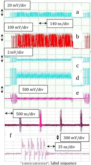
″1100101100101010″: label sequenceFig. 3. Oscilloscope traces for ISOA = 50 mA, Pi = -16 dBm and λ = 1550 nm,
optical burst input (a) and output (b) (after O/E conversion), electrical signal at the output of bias tee (c), RF amplifier (d), HPF (e),
Optical Amplifier SOA-S-OEC-1550 used in the amplifying detection mode and an electronic circuitry which recovers the label signal from the detected signal.
The electrically detected signal is amplified (RF AMP), then filtered using a 150 MHz Low Pass Filter (LPF) in order to keep only the 155 Mbps label signal. A 100 MHz RC High Pass Filter (HPF) acting as a differentiator takes a time derivative of the signal. Then the signal is sent into a high speed comparator with hysteresis (ACDMP 552 from Analog Devices) where the label signal is recovered. Finally it is converted into the LV-PECL format signal to cope with the FPGA board input format. The power consumption of the extractor is about 1.4 W excluding the thermoelectric cooler’s one. The RF amplifier itself consumes nearly 1W. Note that feeding the derivative signal to the comparator’s input can avoid zero level fluctuations issues that are inherent when handling the signal without the DC component.
Fig. 3 shows oscilloscope traces, for an SOA bias current (ISOA) of 50 mA and an input power (Pi) of -16 dBm at λ=1550 nm, corresponding to the optical burst input (a) and the optical burst output (b) (after O/E conversion). Figs. 3c, 3d and 3e are respectively the electrical signals at the bias tee, the RF amplifier and the HPF outputs. Fig. 3f shows the extracted label after the recovery and the LV-PECL adaptation. The bits stream corresponds well to the emitted label sequence. Underdamping trace shown in Fig. 3f stems from an impedance mismatching between the oscilloscope and the LV-PECL output. We can see that the first filtering process is achieved inside the SOA (Fig. 3c) as the detection bandwidth is limited to several hundreds of MHz according to several parameters like input wavelength, optical input power and SOA bias current.
IV. PERFORMANCES OF THE EXTRACTOR
Four extractors were built in order to equip each input port of the L-OBS demonstrator presented in Fig. 1. In order to test the utilization range of the extractor, we have made several tests with various values of optical input power (Pi) and bias current (ISOA) for the SOA of the extractor. The Anritsu MP1810A bursts generator is configured to work at 9.92 GHz which is an integral multiple (i.e. 64) of 155 MHz; thus each bit of label is coded with 64 bits at 9.92 GHz.
Tests were performed with two bursts size: 9920 bits corresponding to the shortest burst duration of 1 µs in the demonstrator and 49600 bits (5 µs bursts). The inter-burst was in both cases equal to 1984 bits during which no signal was transmitted; it corresponds to the shortest inter-burst duration of 200 ns. The goal of the tests was to determine in which conditions of ISOA and/or Pi in the SOA, the bursts were correctly detected. For that purpose we have measured the difference between the theoretical number of bursts emitted by the burst generator (NT) and the effective number of bursts detected (ND) by the CU (FPGA) during a time interval of measurement. As indicated in section II, the burst number (ND) monitoring counter is incremented in the FPGA for each detected burst of each ingress port. We used this counter to
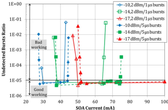
deduce the number of undetected bursts. Then we have plotted the ratio (NT-ND)/NT, which gives the undetected bursts ratio of the couple Label Extractor-CU. According to the quality of the signal at the label output (see Fig. 2), the FPGA is capable or not of detecting the input bursts. If ISOA and Pi are not well chosen, the label bits are distorted and the FPGA is unable to identify and count the bursts up.
We consider that the working range of the LExt corresponds to the range of values of optical input power (Pi) and/or bias current (ISOA) for which the bursts are correctly detected (i.e. the undetected bursts ratio is zero). However due to instabilities in FPGA clock, there is always a small difference when comparing NT to ND. Indeed the clock of the FPGA, which is independent of that of the burst emitter, is not as stable as the bursts emitter’s one as there is no temperature compensation. Its stability is about 10 ppm compared to 1 ppm for the burst generator. Thus observing the detected labels (as in Fig. 3f) and the decisions taken by the CU in terms of output wavelength of the TWC we found that bursts are well detected with an absolute value of undetected bursts ratio lower than 10-5. 1E-06 1E-05 1E-04 1E-03 1E-02 1E-01 1E+00 20 30 40 50 60 70 80 90 100 U n d e te c te d B u rs ts R a ti o
SOA Current (mA)
-10,2 dBm/1 µs bursts -14,2 dBm/1 µs bursts -17,2 dBm/1 µs bursts -10 dBm/5 µs bursts -14 dBm/5 µs bursts -17 dBm/5 µs bursts Good working Bad working
Fig. 4. Undetected bursts ratio versus ISOA for various optical input powers
(Pi) in the extractor for short (1 µs) and long (5 µs) bursts.
Fig. 4 shows the undetected bursts ratio versus ISOA for various input powers (Pi) in the extractor and for 1 µs and 5 µs bursts. Pi is measured with a power meter and corrected to take into account the burst duration and the guard band. It is thus representative of the instantaneous power of the burst at the input of the LExt. We observe that curves shift to higher ISOA when decreasing Pi, the “good working” ranges (for the undetected burst ratio ≤ 10-5) widen when decreasing Pi and are larger for 5 µs bursts than for 1 µs ones. These last results can be explained by considering physical mechanisms underlying changes in the terminal voltage of a constant current driven SOA subjected to an optical signal injection.
It is well known that when an optical signal is injected, the SOA amplifies the input signal. Simultaneously the amplified signal stimulates recombination of carriers in the active layer and depletes the conduction and valence bands resulting in a decrease in quasi-Fermi level separation. This appears as a
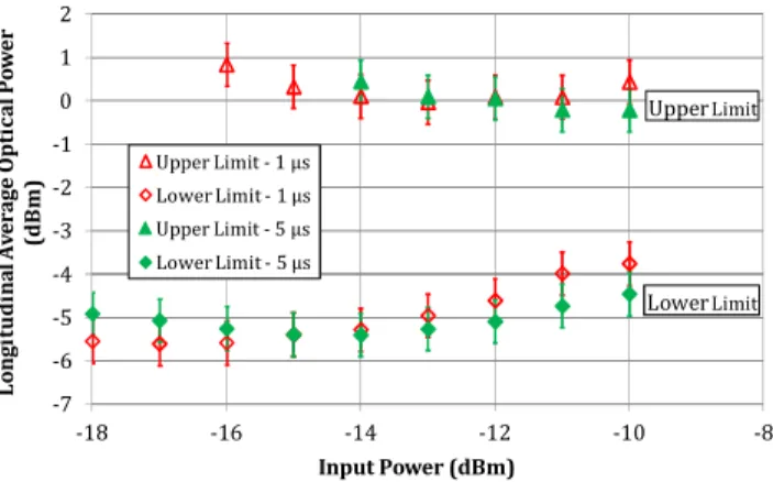
SOA – actual case – changes in the terminal voltage have to be proportional to the spatial average of the optical power in the SOA with the opposite sign. Basically, to obtain a good working range of ISOA, the amount of changes in the terminal voltage (∆V) has to be within the input voltage range of the electronics of the extractor. Therefore finding relationships among ∆V, ISOA and Pi would allow explaining the results. Unfortunately it was not possible to directly measure ∆V without perturbing the experiment. Therefore we explain the results resorting to an estimation of the longitudinal average of optical power inside the SOA instead of ∆V. We approximated the SOA by one dimensional amplifier of which the optical power evolves as exp(gz) with g the gain coefficient, supposed to be constant, z the propagation direction. We calculated the longitudinal average of the optical power with Pi, ISOA and the output power (Pout) for good undetected burst ratios. Fig. 5 shows the longitudinal average optical power inside the SOA for various Pi for the minimum (lower limit) and maximum (upper limit) values of ISOA for which the extractor detects correctly the bursts. Uncertainties coming from experimental components (photodiode, bias current and polarization dependence of gain) are estimated to be about +/- 0.5 dB. As expected when expressing ISOA in terms of longitudinal average power, the curves are roughly independent of Pi and similar for 1 µs and 5 µs bursts. These show that good working ranges (upper limit – lower limit at given Pi) are determined by the input voltage range of the electronics of the extractor and ∆V.
-7 -6 -5 -4 -3 -2 -1 0 1 2 -18 -16 -14 -12 -10 -8 L o n g it u d in a l A v e ra g e O p ti c a l P o w e r (d B m ) Input Power (dBm) Upper Limit - 1 µs Lower Limit - 1 µs Upper Limit - 5 µs Lower Limit - 5 µs UpperLimit LowerLimit
Fig. 5. Longitudinal average optical power inside the SOA versus Pi with upper and lower limit of ISOA for short (1 µs) and long (5 µs) bursts. In order to evaluate the behavior of the Label Extractor in actual conditions, we have plotted in Fig. 6 the undetected burst ratio versus Pi for ISOA = 45 mA and for the two burst sizes studied before. Indeed, in actual configuration the bias current of the SOA included in each extractor is set and bursts that can come from different parts of the network arrive at the input of the LExt and so have different input levels. We can observe that the input power range is 4 dB which proves that the designed extractor is compatible with variations of the input power and the bursts duration in an actual
at the extractor input, another SOA can be used in a saturated configuration in order to limit the variation of the bursts amplitude. The fiber to fiber gain of the SOA is about 8 dB at 45 mA for Pi = -10 dBm and is higher than 17 dB at 100 mA for Pi = -17 dBm which makes the use of such solution of extraction interesting in terms of data path optical budget to compensate for losses inside the node.
1E-06 1E-05 1E-04 1E-03 1E-02 1E-01 1E+00 -18 -17 -16 -15 -14 -13 -12 -11 -10 -9 -8 U n d te c te d B u rs ts R a ti o Input Power (dBm) 1 µs bursts 5 µs bursts 4 dB working range Good working Bad working
Fig. 6. Undetected bursts ratio versus optical input power (Pi) in the label extractor for ISOA = 45 mA.
V. CONCLUSION
We have reported experimental results of a label extractor for Labeled-OBS applications. The extractor which uses an SOA in the amplifying detection mode to extract the label part of a burst with attached payload has the advantage of being completely transparent to the entire optical burst (label plus payload). A working range of more than 25 mA has been observed for an optical input power of -14 dBm with two burst sizes. Moreover a tolerance to the input power fluctuations of 4 dB together with a fiber to fiber gain higher than 8 dB has been demonstrated which validates the use of the designed function in a practical environment.
REFERENCES
[1] T. Legrand, H. Nakajima, P. Gavignet, B. Cousin, "Labelled OBS Test Bed for Contention Resolution Study", presented at 5th International Conference on Broadband Communications, Networks and Systems (BROADNETS), London, UK, Sept. 8-11, 2008.
[2] D. Chiaroni, et al. “Demonstration of the Interconnection of Two Optical Packet Rings with a Hybrid Optoelectronic Packet Router” in Proc. ECOC, 19-23 September 2010, PD 3-5, pp 1-3, 2010.
[3] S.C. Lee, R. Varrazza, S. Yu, “Demonstration of optical label detection and 10 Gbit/s packet routing using 4x4 optical crosspoint switch”, Electron. Letters, vol. 41, no. 8, pp. 491-492, 14th April. 2005. [4] M. Gustavsson, A. Karlsson and L. Thylén, “Travelingwave
Semiconductor Laser Amplifier Detectors”, IEEE J. Lightwave Technol. Vol.8, no.4, pp. 610-617, Apr. 1990.
[5] T. Rampone, “Semiconductor Optical Amplifier Used as an In-Line Detector with the Signal DC-Component Conservation,” IEEE J.
Lightwave Technol., vol. 16, no. 7, pp. 1295–1301, July 1998.
[6] R. M. Fortenberry, A. J. Lowery, R. S. Tucker, “Up to 16 dB Improvement in Detected Voltage using Two-Section Semiconductor Optical Amplifier Detector,” Electron. Letters, vol. 28, no. 5, pp. 474– 476, 27th Feb. 1992.