Pépite | Absorbants électromagnétiques parfaits et large bande à base de métamatériaux
172
0
0
Texte intégral
(2) Thèse de Jianping Hao, Lille 1, 2016 Résumé. Résumé Ce travail de thèse concerne les structures artificielles àbase de métamatériaux permettant la réalisation d’absorbants parfaits. Après une brève introduction des métamatériaux, de leur fonctionnement en tant qu’absorbants et de l’état de l’art, quatre types de structures fonctionnant en bandes centimétrique ou millimétrique ont été conçus puis fabriqués àsavoir (i) des réseaux de cubes BaSrTiO3 (BST) basés sur les résonances de Mie, (ii) des réseaux désordonnés composés d’anneaux métalliques mettant en jeu des effets de résonance semblables aux systèmes plasmoniques (iii) des absorbants àquatre résonateurs élémentaires sur substrat flexible et (iv) des réseaux multicouches métal-diélectrique de forme pyramidale. Pour l’ensemble, des simulations numériques, corroborées par l’expérience en guide d’onde ou en espace libre, montrent l’existence d’un moment magnétique. Celui-ci est induit par une boucle des courants de déplacement et de conduction. Pour les structures périodiques, les conditions de grande largeur de bande d’absorption ont été établies sur la base du piégeage et de la dissipation de l’énergie incidente. Pour les réseaux désordonnés, il est montré le rôle capital des couplages entre résonateurs. Des structures périodiques à base de ferroélectrique de dimensions sous longueur d’onde ont été assemblées avec succès tandis que des absorbants flexibles ont été réalisés par technique d’impression jet d’encre montrant l’amélioration d’un facteur quatre de la bande d’absorption. Des améliorations comparables ont été obtenues à l’aide de réseaux d’anneaux, dont les positions dans le plan sont désordonnées, résultant de la distribution des fréquences de résonance par effet de couplage fort entre les résonateurs.. I. © 2016 Tous droits réservés.. lilliad.univ-lille.fr.
(3) Thèse de Jianping Hao, Lille 1, 2016 Abstract. Abstract In this thesis broadband Metamaterial Perfect Absorbers (MPAs) have been investigated. Following a brief introduction of metamaterials, operating mechanisms and state of the art of MPA, four absorber types operating either at centimeter or millimeter wavelengths have been designed and fabricated namely :(i) Mie-resonance based BaSrTiO3 (BST) arrays operating at microwaves, (ii) plasmonic-type disordered ring-shaped MPA, (iii) four patches millimeter wave flexible absorbers (iv) Pyramidal metal/dielectric stacked resonator arrays. For all the structures, it was demonstrated, through numerical modeling, assessed by characterization in a waveguide configuration or in free space, that unit absorbance relies on magnetic resonances induced by a current loop combining displacement and conduction currents. For periodic arrays, the condition for a broad band operation was established via the optimization of dissipation and trapping of electromagnetic energy in the resonators. For disordered metamaterials, it was shown the major role played by the magnetic dipole-dipole interaction. From the technological side, Ferroelectrics cube arrays with subwavelength dimensions were assembled onto a metal plate while flexible multi-resonators periodic arrays were successfully fabricated by ink-jet printing showing a fourfold enhancement of the absorbance bandwidth thanks to the overlapping of resonance frequencies. Comparable improvement in the bandwidth was also pointed out with randomly position metal ring arrays due to the distribution of resonance frequencies that result from tight in-plane resonator coupling Key words: Metamaterials perfect absorber, Mie-resonance, BST cubes, Plasmonic, Resonators, Pyramid.. II. © 2016 Tous droits réservés.. lilliad.univ-lille.fr.
(4) Thèse de Jianping Hao, Lille 1, 2016 Acknowledgements. Acknowledgements How time flies! Together with my master training section this is already the fifth year of my studying and living in Lille, the one of the most biggest and beautiful cites in the worldly well-known romantic country. I still clearly remember that when I just landed on this strange land in 2011, everything was so fresh and strongly attracted me. While the reality dramatically dragged me to an embarrassed situation--I could not speak French, the most beautiful language over the world. With generous assistances from these graceful people around me, I finished my 6 month training period, which also makes me addict to the environment, life, colleagues and lovely friends here and firmly decide to come back again for a PhD research. Luckily I got this chance, but gradually I realized in such research level it is full of various challenges. I could not imagine how difficult it would be without the support from professors, colleagues, friends and my family, the forever solid background. I would like to thank all of you for guiding me in the research field and helping me in my daily life. First and foremost, I would like to express my sincerest gratitude to my promotor, Prof. Dr. Didier Lippens for approving my work in the training session and providing me this PhD opportunity. I am grateful for his endless and patient guidance, which could be found in every discussion and the long emails with explanation in detail and clearly to-do list. His passion and rigorous attitude on the scientific research was deeply impressed me. Many thanks to my co-promotor Prof. Dr, Eric Lheurette who is not only like a professor but a friend in both my research and my daily life. In the discussions, he could always explain some kind of ‘boring’ stuff in a vivid version. Having lunch together with so many interesting story and French common sense from him made me more love this country and feel a sense of belonging. I would like to thank Prof. Dr. Ludovic Burgnies and Prof. Dr. Veronique Sadaune for guiding me in the simulation and experimental demonstration, III. © 2016 Tous droits réservés.. lilliad.univ-lille.fr.
(5) Thèse de Jianping Hao, Lille 1, 2016 Contents. respectively. Their constant and precious support helped me a lot in my PhD research. I also received a lot of support from our group members: Thanks to the engineers Guillaume Ducournau, Sylvie Laby, Vanessa Avramovic, Etienne Okada, Colin Mismer and et. al.. who helped me fabricate the sample, built the setup and conducted the experiments. I learnt a lot of practical skills from them which will be surely helpful in my future career. Thank Malika Habba, Valerie Mikolajczy and et. al. for devoting your time to fix my troubles. I would like to thank my former master supervisor Prof. Dr. Hou Jianping and Prof. Dr. Zhang Fuli for assisting me to grasp the chance of the master training in Prof. Dr. Didier Lippens’ group. A special section goes to our big chinese group in IEMN: Zhu Tianqi, Gu Sijia, Ding Xiaokun, Weiwei & Zhou Di, Zhang Tianchen, Lin Tianjun, Li Shuo. Chen Shiqi, Xu Tao and et. al.. Thank you all for making me feel like living in a family. Finally, heartfelt thanks to my family for their endless love and moral support. They always raise me up when I was low. Any of my success contains their devotions and they deserve any of the honors I received. Thanks to my husband, Zhang Jing for encouraging me all the time. I would not focus on my work without his great effort on dealing with all the issues in my life. Thanks to my little girl, Zhang YiXin who bring me so much happy time in the last period of my PhD. Jiaping HAO In Lille France 05/10/2016. IV. © 2016 Tous droits réservés.. lilliad.univ-lille.fr.
(6) Thèse de Jianping Hao, Lille 1, 2016 Contents. Contents Resume .......................................................................................... I Abstract ....................................................................................... II Acknowledgements .................................................................... III Contents ...................................................................................... V List of figures .............................................................................. X List of tables ............................................................................ XIV Introduction .................................................................................. 1 Chapter 1 Background and context ............................................. 5 1.1 Motivations ....................................................................................5 1.2 Introduction to meta-materials .......................................................5 1.3 Principle of perfect meta-material absorbers .................................7 1.3.1 Mie-resonance based perfect meta-material absorber .......................... 8 1.3.2 Plasmonic based perfect meta-material absorber ............................... 10. 1.4 Overview of the state of the arts ..................................................11 References ..........................................................................................13. Chapter 2 Ferroelectrics based perfect absorbers ...................... 23 2.1 Introduction ..................................................................................23 V. © 2016 Tous droits réservés.. lilliad.univ-lille.fr.
(7) Thèse de Jianping Hao, Lille 1, 2016 Contents. 2.2 BST periodic array single band perfect absorber ........................24 2.2.1 Design of the periodic absorbing layers ............................................. 24 2.2.2 Influence of material properties ......................................................... 28 2.2.3 Influence of geometry ........................................................................ 30 2.2.4 Incidence angle and polarization analysis .......................................... 37 2.2.5 Experimental verification ................................................................... 39. 2.3 Giant causeway-like absorbers based on size dispersion of ferroelectric Mie type resonators .......................................................46 2.3.1 Design and analysis of the broadband absorbing layer ...................... 46 2.3.2 Experimental verification ................................................................... 51. 2.4 Bandwidth enhancement by BST randomly positioned absorber54 2.4.1 Design and simulation analysis .......................................................... 54 2.4.2 Characterization in free space ............................................................ 56. 2.5 Conclusion ...................................................................................58 References ..........................................................................................59. Chapter. 3 Broadband. perfect. absorbers. in. disordered. meta-materials ............................................................................ 65 3.1 Introduction ..................................................................................65 3.2 Periodic steel rings array..............................................................67. VI. © 2016 Tous droits réservés.. lilliad.univ-lille.fr.
(8) Thèse de Jianping Hao, Lille 1, 2016 Contents. 3.2 .1 Magnetic response in steel rings resonators ...................................... 67 3.2 .2 Influence of incidence angle .............................................................. 73. 3.3 Random meta-material based absorbers ......................................77 3.3.1 Influence of the coupling forces between resonators in random meta-materials .............................................................................................. 77 3.3.2 Influence of the filling factor in random metamaterials ..................... 79 3.3.3 Influence of the contact between elementary rings ............................ 82 3.3.4 Oblique incidence influence ............................................................... 84 3.3.5 Experimental verification ................................................................... 87. 3.4 Conclusion ...................................................................................96 References ..........................................................................................97. Chapter 4 Bandwidth enhancement of flexible multi-size resonator arrays at millimeter waves ....................................... 101 4.1 Introduction ................................................................................101 4.2 Bandwidth enhancement of flexible multi-size resonator arrays at millimeter waves ..............................................................................103 4.2.1 Design of the structure and simulation analysis ............................... 103 4.2.2 Equivalent circuit mode analysis ...................................................... 108 4.2.3 Fabrication ........................................................................................ 111 4.2.4 Experimental verification in free space ............................................ 113 VII. © 2016 Tous droits réservés.. lilliad.univ-lille.fr.
(9) Thèse de Jianping Hao, Lille 1, 2016 Contents. 4.3 Conclusion .................................................................................116 References ........................................................................................117. Chapter 5 Stacked Plasmonic resonator based millimeter wave absorber .................................................................................... 121 5.1 Introduction ................................................................................121 5.2 Design of the pyramid millimeter wave ultra-broadband absorber ..........................................................................................................122 5.2.1 Parametric analysis ........................................................................... 125 5.2.2 Dispersion diagram analysis ............................................................. 129. 5.3 Conclusion .................................................................................131 References ........................................................................................131. Chapter 6 Wave controlling device: the example of a woodpile structure .................................................................................... 135 6.1 Introduction ................................................................................135 6.2Primary results of woodpile structures .......................................135 6.3Discussion about GRIN lens .......................................................141 6.4 Conclusion .................................................................................143 References ........................................................................................143 VIII. © 2016 Tous droits réservés.. lilliad.univ-lille.fr.
(10) Thèse de Jianping Hao, Lille 1, 2016 Contents. Conclusions and Prospects ...................................................... 145 List of publications .................................................................. 149. IX. © 2016 Tous droits réservés.. lilliad.univ-lille.fr.
(11) Thèse de Jianping Hao, Lille 1, 2016 List of figures. List of figures Fig. 1.1 Electric (y-z plane) and magnetic (x-z plane) field distributions in a dielectric cube with sidewidth a = 1.8 mm at the first Mie resonance frequency 11.14 GHz. ······························································10 Fig.2.2.1 Schematic layout of (a) the metamaterial absorber with illustration of the TE and TM polarization modes of the incident wave and the definition of incidence angle (b) The basic unit cell with its characteristic parameters and the simulation conditions (c) Photograph of the periodic BST 2D array. .... 25 Fig.2.2.2 Reflection and absorption spectra for an absorber with BST cube array with period Px = Py = 9mm and side length ax = ay = az = 1.8 mm on a 0.2 mm-thick dielectric layer and a metal substrate. ......................................... 26 Fig.2.2.3 E and H vector recorded for the two resonance peaks at the center of the cubes, respectively. ...................................................................................... 27 Fig.2.2.4 Dispersion characteristic for BST array absorber with p = 9 mm. Highly localized eigen-states of the BST magnetic resonator are square in light blue, rose, and orange symbols around the magnetic travelling surface wave (in dark blue square symbol). The black dot line represents the propagating wave. ...................................................................................................................... 28 Fig.2.2.5 Absorption spectra for BST cube array with side length = 1.8 mm and period = 9 mm, interfaced with a 0.2 mm-thick dielectric with a metal plate(infinite conductivity) for BST permittivity varying from 100 to 160 (a), for BST loss tangent varying from 0.005 to 0.05 (b), (c) FWHM and Q factor dependence as a function of tan. ................................................................ 29 Fig.2.2.6 Influence on the absorption by a dielectric spacer with thickness d varying from 0 mm to 4 mm, with BST permittivity equal to 132(1+0.02i), P equals to 9 mm. ............................................................................................ 31 X. © 2016 Tous droits réservés.. lilliad.univ-lille.fr.
(12) Thèse de Jianping Hao, Lille 1, 2016 List of figures. Fig.2.2.7 E vector distribution in BST cubes with d = 0.0 mm and d = 0.2 mm in y-z plane, respectively. ................................................................................. 32 Fig.2.2.8 H field map in x-z plane with d = 1.0 mm, 3.0 mm and 4.0 mm at resonance frequency, respectively. ............................................................... 33 Fig.2.2.9 Influence on the absorption by BST size ax (a), ay (b), az (c) varying from 1.4 mm to 2.6 mm, with BST permittivity equal to 132(1- 0.02i), P equals to 9 mm, (d) resonance frequency dependence of BST size. ........................... 34 Fig.2.2.10 Influence of the period of the BST cubes (ax = ay = az = 1.8 mm) array (p = px = py) on the absorption spectra for p varying from 3 mm to 19 mm. Maximum of absorbance versus the array period is plotted in the left. ....... 35 Fig.2.2.11 Dispersion characteristics versus the in plane vector of various periods. ...................................................................................................................... 36 Fig.2.2.12 (a) Maximum absorption as a function of period, (b) Q factor as a function of frequency, for loss tangent ranging from 0.005 to 0.05. ........... 37 Fig.2.2.13 Absorption spectra as function of frequency for incidence angle ranging from 0o to 75o for TE (a) and TM (b) modes, respectively. ............ 38 Fig.2.2.14 shows the S11 spectra obtained in the test, (a) measured in X band wave guide, (b) measured in Ku band wave guide, insert is the zoomed view of S11 parameters from 15 to 17 GHz..................................................................... 40 Fig.2.2.15 Schematic of the hollow metal waveguide configuration for assessing the coupling effect, PH and PE definition. .................................................. 41 Fig.2.2.16 Simulated and experimental reflection spectra for BST cubes dimer when varying PH ranging from 2 mm to 11 mm. ........................................ 41 Fig.2.2.17 E and H vector at resonance frequency in the center of the cubes in y-z and x–z plane, (a) for PH = 2 mm and (b) for PH = 6 mm, respectively. .... 43 XI. © 2016 Tous droits réservés.. lilliad.univ-lille.fr.
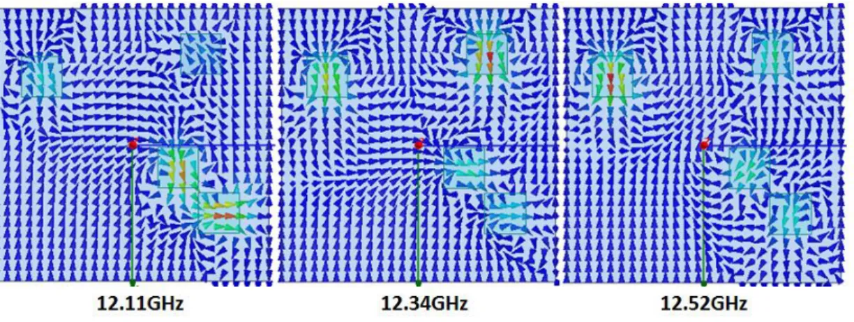
(13) Thèse de Jianping Hao, Lille 1, 2016 List of figures. Fig.2.2.18 (a) Experimental and (b) simulated reflection spectra for BST cubes dimer when varying PE ranging from 2 mm to 7 mm. ................................ 43 Fig.2.2.19 E and H vector at resonance frequency in the center of the cubes in y-z and x–z plane, (a) for PE = 2 mm and (b) for PE = 6 mm, respectively. ..... 44 Fig.2.2.20 (a) schematic view of the experimental set-up in free space, (b) the experiment S11 spectra of BST cubes (with the side width around 1.8 mm) arrayed on the copper plate which measured under normal incidence in the free space condition. .................................................................................... 45 Fig.2.3.1 Schematic of a network of cubes of different heights BST (a), (b) the rocky structures of the Giant's Causeway, (c) Window of absorption calculated for a network of 9 absorbing centers .......................................... 48 Fig.2.3.2 The E-field magnitude is plotted in the BST mid-plane, for the configuration corresponding to the optimized period P = 12 mm at (a) 12.0 GHz, (b) 12.5 GHz, (c) 12.95 GHz. ............................................................. 49 Fig.2.3.3 Schematics of an array of 16 BST cuboids with four different heights (a) 1, 2, 3 and 4 arrangement, (b) 1, 4, 2 and 3 arrangement for the first row. . 50 Fig.2.3.4 Absorption window calculated for two different arrangement (1234 and 1423 configurations) of an absorber consisted of 16 resonators in the super-cell. ..................................................................................................... 50 Fig.2.3.5 Schematic of an array of 16 BST cuboids with 16 different heights from 1.4 mm to 2.6 mm randomly varied (left figure). Absorption spectrum as a function of frequency for three different configurations (right figure). ....... 51 Fig.2.3.6 Schematic of the simulation domain mimicking an X-band wave guide loaded by the absorber basic cell and boundary conditions (left-side). Photograph of the flange of an X band wave guide associated to a single micro-resonator positioned on a metal plate by using adhesive (right-side). XII. © 2016 Tous droits réservés.. lilliad.univ-lille.fr.
(14) Thèse de Jianping Hao, Lille 1, 2016 List of figures. ...................................................................................................................... 51 Fig.2.3.7 Comparison between experimental and simulation results for single BST rectangular with various heights ranging from 1.8 mm to 3.0 mm.............. 52 Fig.2.3.8 Schematic of the basic cell in X-band wave guide and the simulation conditions (left). Photograph of the 8 BST rectangular arrays. Photo of X band waveguide completed with eight micro-resonators deposited on a metal plane (right). ................................................................................................. 53 Fig.2.3.9 Illustration of the results of measurements and simulation for absorber consisting of ferroelectric elements whose longitudinal dimensions have been distributed as 1.8 mm, 2.5 mm, 2.62 mm, 2.8 mm, 2.82 mm, 2.9 mm, 2.96 mm, 3.0 mm. ........................................................................................ 54 Fig. 2.4.1 Schematic of the basic super-cell in the top view (left) and the simulation conditions (right). ....................................................................... 55 Fig. 2.4.2 The absorption spectrum as a function of the frequency for random and periodic (P = 6 mm) structure as shown in Fig.2.4.1, the BST cubes with the side length of 1.8 mm................................................................................... 56 Fig. 2.4.3 H-vector for random structure at frequency 12.11 GHz, 12.34 GHz and 12.52 GHz, respectively. .............................................................................. 56 Fig. 2.4.4 (left) Photograph of the random BST cubes (side length around 1.8 mm) sample deposited on the copper plate, (right) schematic illustration of measurement set up. ..................................................................................... 57 Fig. 2.4.5 Experimental absorption spectrum for the random structure in figure 2.4.4 (left)..................................................................................................... 58 Fig. 3.2.1 Schematic of the basic resonator (a) top view with its characteristic parameters (b) Illustration of simulation conditions. ................................... 68 XIII. © 2016 Tous droits réservés.. lilliad.univ-lille.fr.
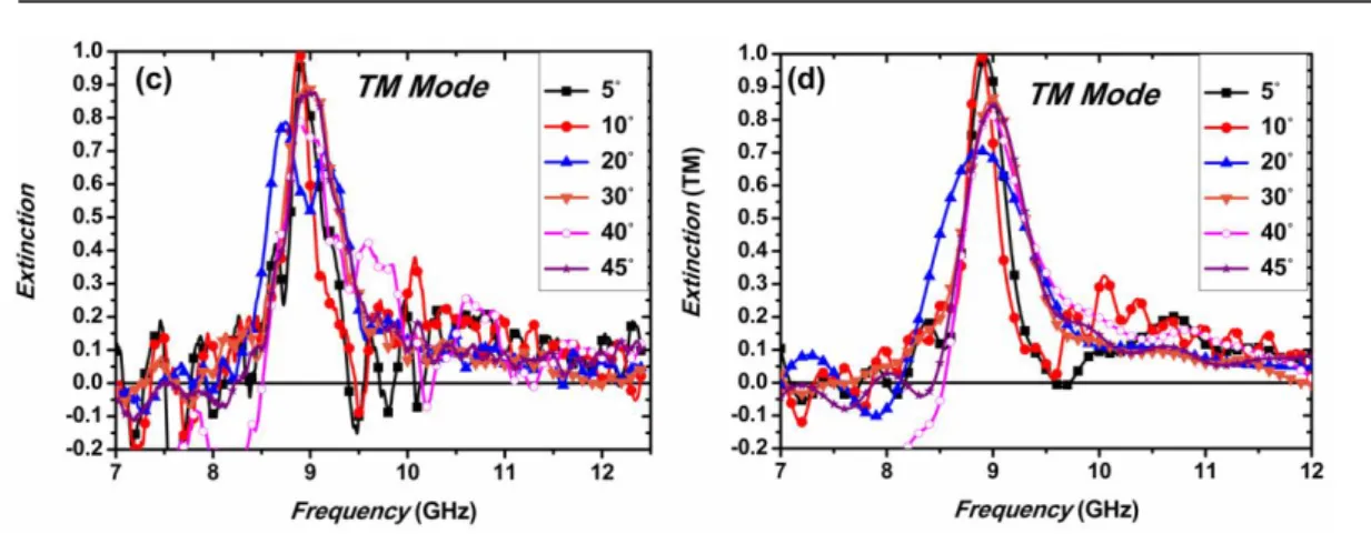
(15) Thèse de Jianping Hao, Lille 1, 2016 List of figures. Fig. 3.2.2 (a) Extinction spectrum simulated for a periodic array of rings deposited on a metal-coated Epoxy substrate. The fundamental magnetic resonance mode occurs at 9.11 GHz as illustrated by the field maps showing (b) the electric field vector and (c) the magnetic field vector. These maps are plotted in the mid plane between the steel ring and the ground plane. .................... 69 Fig. 3.2.3 (a) Schematic of the measurement equipment operating in X-band, (b) Peak absorbance detected around 9 GHz as a function of the array period. Insert is a photograph of a measured array. ................................................. 70 Fig. 3.2.4 Schematic of the incidence angle definition and the simulation conditions. .................................................................................................... 73 Fig. 3.2.5 Absorption spectra with respect to frequency (a) for TE mode, (b) for TM mode. ..................................................................................................... 73 Fig. 3.2.6 (a) Schematic view of the experimental set-up, (b) Photograph of the measured period rings array. ........................................................................ 74 Fig. 3.2.7 Wave extinction (a) for TE mode without time-domain process, (b) for TE mode with time-domain process, (c) for TM mode without time-domain process, (d) for TM mode with time-domain process. ................................. 76 Fig. 3.3.1 (a) Extinction spectra for 5 different positions of the ring resonator within a 24 x 24 mm2 unit cell bounded by perfect mirror conditions. The Poynting vector is plotted in the dielectric mid-plane, for the configuration corresponding to the black-dotted curve, at each maximum: (b) 8.54 GHz, (c) 8.81 GHz. ..................................................................................................... 78 Fig. 3.3.2 Schematic of the resonators randomly position on the FR-4 substrate and the simulation conditions ...................................................................... 80 Fig. 3.3.3 Extinction spectra simulated for various filling factors within a 48 x 48 mm2 unit cell bounded by perfect mirror conditions and the distribution of the XIV. © 2016 Tous droits réservés.. lilliad.univ-lille.fr.
(16) Thèse de Jianping Hao, Lille 1, 2016 List of figures. various cases (a) 10 %, (b) 20 %, (c) 30 % and (d) 40 %. (e) Average extinction calculated between 7 and 11 GHz for the various case depicted in Fig. 3.3.3 (a) to (d). ...................................................................................... 82 Fig. 3.3.4 (a) Extinction spectra for various position of four ring resonators within a 48 x 48 mm2 unit cell bounded by perfect mirror conditions. The E-field magnitude is plotted in the dielectric mid-plane, for the configuration corresponding to the black curve at (b) 3.73 GHz (marker 1), (c) 9.82 GHz (marker 2) and configuration corresponding to the red curve at (d) 7.96 GHz (marker 3), (e) 9.06 GHz (marker 4)............................................................ 83 Fig. 3.3.5 (a) Extinction spectra versus frequency under oblique incidence (TM mode) for a 48 x 48 mm2 unit-cell including 15 resonators and bounded by master-slave conditions, E-field magnitude in the dielectric mid-plane at 8.9 GHz and 15°incidence angle for TE (b) and TM (c) polarization, incident E-field direction shown by red-arrows, (d) average extinction spectra versus incidence angle plotted for both polarization directions along with the average cross-polarization reflectance. ........................................................ 86 Fig. 3.3.6 Photograph of the measured structure for the 4 random configurations. ...................................................................................................................... 88 Fig. 3.3.7 Comparison between the optimal periodic case (24 mm) and various random structures by keeping the number of rings (96) constant. ............... 89 Fig. 3.3.8 Photograph of the measured structure for the six different number rings distribution. .................................................................................................. 90 Fig. 3.3.9 Absorbance versus frequency measured for randomly distributed metamaterials structure with number of rings ranging from 51 to 371. ...... 91 Fig. 3.3.10 Electric field map in the dielectric mid-plane for a random 10 rings super-cell at 7.85 GHz (a), 8.40 GHz (b), and 8.95 GHz (c). ...................... 91 XV. © 2016 Tous droits réservés.. lilliad.univ-lille.fr.
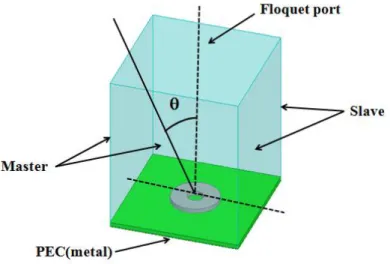
(17) Thèse de Jianping Hao, Lille 1, 2016 List of figures. Fig. 3.3.11 Schematic view of the experimental set-up. Be careful: the TE mode triedron is also left-handed here. .................................................................. 92 Fig. 3.3.12 (a) Photograph of the tested structure, Extinction spectra measured for a random structure including 100 rings in a 21 x 29.7 cm2 grounded substrate as a function of the incidence angle (b) TE polarization, (c) TM polarization. ...................................................................................................................... 93 Fig. 3.3.13 (a) Photograph of the tested structure, Extinction spectra measured for a random structure including 200 rings in a 21 x 29.7 cm2 grounded substrate as a function of the incidence angle (b) TE polarization, (c) TM polarization. ...................................................................................................................... 94 Fig. 3.3.14 (a) Photograph of the tested structure, Extinction spectra measured for a random structure including 300 rings in a 21 x 29.7 cm2 grounded substrate as a function of the incidence angle (b) TE polarization, (c) TM polarization. ...................................................................................................................... 95 Fig. 3.3.15 (a) Photograph of the tested structure, Extinction spectra measured for a random structure including 400 rings in a 21 x 29.7 cm2 grounded substrate as a function of the incidence angle (b) TE polarization, (c) TM polarization. ...................................................................................................................... 95 Fig.4.1 (a) 3D schematic of the super-cell square-lattice array with square-shaped metal/dielectric metal resonator (b) top view of the super-cell, (c) cross section of the three layered metal pattern /dielectric spacer layer/ ground metal plate, (d) the super-cell with its characteristic parameters and the simulation conditions. ................................................................................ 104 Fig.4.2 Absorbance spectrum (red line) determined from the scattering parameter S11 (blue line) calculated by full wave analysis (a), illustration of the influence of the incidence angle (θ) (b). .................................................... 105 XVI. © 2016 Tous droits réservés.. lilliad.univ-lille.fr.
(18) Thèse de Jianping Hao, Lille 1, 2016 List of figures. Fig.4.3 (a) The surface current distribution in the x-y plane on the top and bottom metal surface, (b) Poynting vector map in the x-y plane at the middle of the dielectric layer at f2 (left-side) and f3 (right-side) respectively. ................. 107 Fig.4.4 Schematic of the equivalent circuit mode.............................................. 108 Fig.4.5 Schematic of the TLM-based simulation condition .............................. 109 Fig.4. 6 Frequency dependence of the complex impedances ZFSS, Zd and Ztot. .. 109 Fig.4.7 Total impedance of the four different size parts as di = 1 mm, 0.945 mm, 0.890 mm and 0.850 mm. .......................................................................... 110 Fig.4. 8 Variation of the total complex impedance of the super-cell array. ....... 111 Fig.4.9 (a) Photograph of the absorbing device fabricated with a 30 ×30 mm2 area. (b) Illustration of the flexibility of the sample, (c) optical photograph of the four silver lumps on top view..................................................................... 113 Fig.4.10 (a) Close view of the free-space set up used for the vector network analysis in the 75-110 GHz W-band, (b) illustration of the TE and TM polarization in the measurement, (c) schematic diagram of the free-space set up ............................................................................................................... 114 Fig.4.11 Experimental (blank line Mirror as reference, red line PET substrate with Al metallic ground as reference) and simulation (blue line) absorption spectra under normal incidence, (a) TE polarization, (b) TM polarization. ........... 115 Fig.4.12 Photograph of the free-space set up of vector network analysis in the 75-110 GHz band used for the oblique incidence measurement. .............. 116 Fig.4.13 Experimental absorption spectra under obilque incidence vared from 0°to 30°of TE polarization. ........................................................................ 116 Fig. 5.1 Design of a millimeter wave ultra-broadband PMA, (a) 3-D illustration of the simulation PMA in periodic array, (b) schematic of a PMA unit cell, and XVII. © 2016 Tous droits réservés.. lilliad.univ-lille.fr.
(19) Thèse de Jianping Hao, Lille 1, 2016 List of figures. (c) zoomed view of the sub-elemental cell. ............................................... 123 Fig. 5.2 Absorption and reflection curves with the dimensions of a unit are Wt = 0.315 mm, Wb = 0.6 mm , P = 0.8 mm, T = 0.65 mm, dm = 15m, dg = 35m. .................................................................................................................... 124 Fig. 5.3 Simulated electric and magnetic amplitude distributions at the central cross section of a unit cell in y-z plane at three resonance frequencies. .... 125 Fig. 5.4 Absorption coefficient with respect to frequency for four periods ranging from 0.7 mm to 1.0 mm. ............................................................................ 126 Fig. 5.5 Absorption coefficient with respect of frequency (a) for thickness of dielectric t1 from 15 m to 55m while t2 =15 m constant, (b) for thickness of metal t2 varied from 5 m to 25 m while t1=35 m constant. ............. 127 Fig. 5.6 Absorption coefficient with respect of frequency (a) for bottom lengths Wb ranging as 0.5 mm, 0.6 mm and 0.7 mm, (b) with different number of resonator layers ranging as 7, 10, 13 and 15 layers. .................................. 128 Fig. 5.7 Absorption coefficient with respect to frequency, (a) under influence of dielectric loss tangent varying from 0 to 0.1, (b) under influence of metal conductivity ranging from 4×10⁵ S/m to 4×10⁷ S/m. ................................. 129 Fig. 5.8 Simulation domain used for the dispersion calculation. ....................... 130 Fig. 5.9 (a) dispersion curves when W varied as 0.3, 0.4, 0.5 and 0.6 mm, (b) corresponding absorption lines. ................................................................. 130 Fig. 5.10 Dispersion curves of the pyramid PMA. ............................................ 131 Fig. 6.1 Schematic of woodpile photonic crystal structures (left), diagram of the super-unit cell (right). ................................................................................ 136 Fig. 6.2 The transmission spectrum of k along the direction parallel to the stacking(16 rods) direction, with w = 1.25mm, for TE and TM modes, XVIII. © 2016 Tous droits réservés.. lilliad.univ-lille.fr.
(20) Thèse de Jianping Hao, Lille 1, 2016 List of figures. respectively, insert is the simulation schematic with the Master and Slave period boundary conditions........................................................................ 137 Fig. 6.3 Transmission spectra for incident k vector parallel to the stacking direction for TE mode, for rods widths w varying from 0.25 mm to 1.25 mm. .................................................................................................................... 138 Fig. 6.4 Photograph of the prototype(a), details of the alternating structure(b). 139 Fig. 6.5 Photograph of the free-space set up of vector network analysis in V-band .................................................................................................................... 140 Fig. 6.6 Transmission coefficients S21_Sample of measuring with sample, S21_Ref of without sample, for incidence wave impinge parallel to the stacking direction. ...................................................................................... 141. XIX. © 2016 Tous droits réservés.. lilliad.univ-lille.fr.
(21) Thèse de Jianping Hao, Lille 1, 2016 List of tables. List of tables Table 1 Overview of the state of the art of the broadband absorbers........................... 12. XIV. © 2016 Tous droits réservés.. lilliad.univ-lille.fr.
(22) Thèse de Jianping Hao, Lille 1, 2016 Introduction. Introduction Metamaterials are artificial microstructures that exhibit singular properties not found with natural materials. For electromagnetic metamaterials, the most famous property is the possibility to synthesize a composite material whose effective refractive index that can be defined owing to the deep sub-wavelength structuring relevant dimension, is negative. Under this condition, a wave impinging onto a flat interface between a positive/negative index under tilted incidence exhibits a negative refraction The incident wave is transmitted with a negative angle with respect to the incident one. For a flat lens made of a negative index material also called DNG for Double NeGative material, facing a diverging-ray source, this negative refraction leads to a focusing point inside and outside the lens whatever the position of the source. This singular property, namely focusing of electromagnetic waves with a flat lens with uniform negative index was reported theoretically in the seminal article of Veselago in 1968. In practice however, it was in the 2000s that such negative refraction was further studied theoretically by Pendry with the super lens concept and was demonstrated experimentally by Smith et al. For this experimental verification Negative Index Materials (NIMs), operating at microwaves, were fabricated with periodic arrays of continuous or cut wires and the so-called Split Ring Resonators (SRR). It can be shown that the latter ensures a negative effective permeability by exploiting the phase shift above the resonant frequency. Since these pioneering works, many other ‘metadevices’ were reported in the literature exploiting the electromagnetic properties of metamaterials and notably the so-called Perfect Metamaterial Absorbers (PMA ) that is the main concern of this thesis. By the term perfect, we mean a device that totally absorbs the incident wave energy and thus without any backscattered and transmitted waves. Such an overall absorption of 100 % can be achieved with conventional technology and notably by using the so-called Dallenbach screen made of natural dielectric material (electric or 1. © 2016 Tous droits réservés.. lilliad.univ-lille.fr.
(23) Thèse de Jianping Hao, Lille 1, 2016 Introduction. magneto-electric material) grounded with a uniform metal plate. For these conventional absorbers, which are widely used in the current systems, it can be shown that their thickness has to fit a quarter wavelength. This design criterion is particularly penalizing for absorber operating in the low frequency part of the microwave spectrum. The drawback of rather thick absorbers has thus motivated to look for solutions making use of metamaterial technology by reminding that their relevant dimensions are very small with respect to the operating wavelength. As a consequence, low profile absorber with ultra-thin dielectric layer can be foreseen with also improvements in terms of weight and conformability. In addition the fact that metamaterial are made of resonator array has opened the way to enhance absorption properties at a specific resonant frequency even if the background loss sources is small (in practice a loss tangent of a few percent for microwave absorbers dominated by dielectric losses). In counterpart, conventional PMA’s absorb in a narrow band. This can be a critical issue notably for radar application systems that require a broad absorbance window. In this context, the main objective of this thesis is to provide solutions to this broadband operation issue targeting also the fabrication of low profile, light weight and flexible absorbers Towards these goals we will investigate two kinds of technology (plasmonic– and Mie resonance–type) and several solutions notably based on periodic and disordered arrays by according to the following approach: After a brief introduction where the two technologies and their underlying physical effects are outlined along with a review of the state of the art (chapter 1) Mie resonance based absorbers will be considered in chapter 2. In a first section, millimeter-sized ferroelectric cubes array with a permittivity in excess of 100 will be designed for the achievement of a unit absorbance at centimeter wave length (in practice at X band). Despite the fact that the incident wave is absorbed locally in a long wave length regime, surprisingly in these preliminary studies, it will be shown 2. © 2016 Tous droits réservés.. lilliad.univ-lille.fr.
(24) Thèse de Jianping Hao, Lille 1, 2016 Introduction. that the period of the array plays a major role. Its influence will be clarified on the basis of the balance between the coupling of the incident wave and of the dissipation processes when the energy is trapped in the full dielectric resonators. An experimental assessment, which will be carried out in a wave guide configuration, will demonstrate a unit absorption window in agreement with theoretical prediction. In a second stage we will study the possibility to broaden the band by a distribution of the longitudinal resonator dimension. This solution, termed giant’s causeway absorber in this thesis, owing that a 3-D disordered configuration resembles to that of the balsamic stone field in Ireland, is also assessed experimentally by means of free space measurements. Chapter 3-4 and 5 are devoted to plasmonic PMA’s. For broadening the absorbance bandwidth, we first study the effect of position disorder in metal /dielectric/metal layer that will be the generic structures all along these three chapters. By introducing some disorder in the position of resonators, we strengthen their coupling. It results from the magnetic and electric dipole coupling, a distribution of the resonant frequencies and hence an improvement of the absorbance window. These coupling effects, at the origin of the bandwidth enhancement, are illustrated via numerical simulations and experimentally assessed via the measurement of the frequency dependence of the return loss in free space. In Chapter 4, we will investigate how to broaden the transmission window of an absorber operating at W band (75-110 GHz), targeting the realization of flexible perfect absorber at millimeter wave length. Beside this increase in operating frequencies the solution developed here will be to introduce a multi-size basic cell with slightly different resonant dimension, so that the overlap of the absorbance window broadens the absorption spectrum. Here again an experimental assessment in free space will be carried out for PMA fabricated by ink jet printing technologies. This idea of multi-size absorber will be at last investigated numerically in chapter 5 by considering pyramidal–shaped structures designed for the V and W bands. The specificity of the operation of such stacked structure will be illustrated with a sequential energy trapping pointed out in the field 3. © 2016 Tous droits réservés.. lilliad.univ-lille.fr.
(25) Thèse de Jianping Hao, Lille 1, 2016 Introduction. maps plotted in the cross section along the incidence direction. At last, chapter 6 is very prospective aiming at investigating the technological possibilities recently afforded by the so-called additive technology namely 3D printing. For this preliminary technological study, we chose the example of a wood pile structure whose frequencies cut-off engineering can be used for tailoring the refractive index. Some connections can be established with the development of absorbing metasurfaces notably the possibility to realize ultra-thin meta-device but this is mainly the technological common denominator that are seek.. 4. © 2016 Tous droits réservés.. lilliad.univ-lille.fr.
(26) Thèse de Jianping Hao, Lille 1, 2016 Chapter 1 Background and context. Chapter 1 Background and context 1.1 Motivations In this first part, we will point out the motivation of the whole thesis. In recent years, stealth devices have attracted great interest, the stealth devices also called cloak devices is a theoretical or future technology that can make objects invisible by guiding the incident energy around the object to be hidden or with total absorption. The first experimental electromagnetic cloaking of invisibility at microwave frequency was demonstrated by D. Schuring et al. [1], the cloak was constructed according to use of artificially structured metamaterials by using transformation optics method to control the electromagnetic wave [2-3]. Since then, many other groups have reported a large number of works on this topic [4], including a full dielectric cloak device investigated by D. P. Gaillot et al. by employing BST rod working in microwave and terahertz frequency [5]. However, it is well known that the main drawbacks of cloaking devices are (i) their very narrow band, (ii) their difficulty of realization with extreme values of the permittivity and permeability tensors and (iii) their modest result in terms of Scattering Cross Section reduction. This has motivated the so-called ground cloak which permits one to mimic the reflection of flat surface by mirage effects [6]. However the more classical mean for stealth is the use of absorbers which is the conventional solution used up to now in real life application and which will be used all along this thesis.. 1.2 Introduction of meta-materials Metamaterial are artificial structures that extend the range of electromagnetic properties beyond those available in conventional naturally materials. Such kinds of materials are usually made of assemblies of multiple elements at scales that are much 5. © 2016 Tous droits réservés.. lilliad.univ-lille.fr.
(27) Thèse de Jianping Hao, Lille 1, 2016 Chapter 1 Background and context. smaller than the wavelength, and exhibit singular dispersion properties such as negative permittivity (eff) and permeability (eff) [7-9]. Thanks to these beneficial properties, metamaterial can be used to manipulate electromagnetic waves by absorbing, filtering, enhancing or bending waves. As a consequence, extensive potential applications are foreseen as microwave and optical filters, high sensitivity detectors, low profile directive antennas, right- and left handed phase shifters, invisibility cloaks, ultra-thin total absorbers and so on [10-39]. Obviously, eff and eff are the fundamental parameters which determine the propagation of electromagnetic waves in these artificial composite materials. For metamaterials both effective permittivity and permeability can be negative and the pioneering work on such Double NeGative (DNG) materials was reported by Veselago in 1968 [40]. In this work, Veselago demonstrated that such DNG material exhibits negative refractive index, thus negative phase velocity and named them Left Hand Material (LHM). However at that time there was no materials manifest both negative permittivity and permeability, as it is well known that nature dielectric materials have positive permittivity and permeability, and plasma-type materials exhibit negative permittivity. Until the year 2000, left handed materials were experimentally realized from metallic structures such as periodic arrays of thin metallic wires and open metallic rings (called SRR or Split Ring Resonators) [9, 41-43]. Among these structures, the thin wires gave negative permittivity, and the split rings provided negative permeability. As a kind of renewed artificial materials, metamaterials have been developed rapidly during the two decades. How the realization of metamaterials is one of the most challenging topics, and common metamaterials structure are listed below. Normally, metamaterials can be realized through several kinds of structures: such as photonic crystal structures [45-49], Transmission line (TL) based structures [50-56], resonant structures [40-44], and full dielectric materials [57-58].. 6. © 2016 Tous droits réservés.. lilliad.univ-lille.fr.
(28) Thèse de Jianping Hao, Lille 1, 2016 Chapter 1 Background and context. Generally, photonic crystals are composed of dielectrics, metals, superconductor and semiconductor microstructures, periodically arrayed in one-, two- or three dimensions of space. By this periodic structuring, control of electromagnetic wave propagation can be achieved notably by introducing a forbidden band gap in the dispersion band diagram. As pointed out in Ref. 48 photonic crystal structures have pass–bands with parallel or anti parallel configuration of the phase and group velocity and stop- bands. In Transmission Line (TL) structures, a negative phase velocity regime can also be obtained by loading a conventional printed circuit board TL with series capacitances and shunt inductances. It results from this effective permittivity and permeability simultaneously negative as analytically and experimentally demonstrated by G. Eleftheriades. Resonant structures involve electric and magnetic resonances. For the latter below the electric plasma resonance frequency, the induced magnetic field (B) created by a current loop resulting from the incident magnetic field (H) yields a negative permeability µ (. . By the same principle, electric resonance structures can. provide negative permittivity [7, 44]. Therefore, combining electric and magnetic resonances can give simultaneously both negative permittivity and permeability [9].. 1.3 Principle of perfect meta-material absorbers Perfect metamaterial absorbers (PMA) have attracted great interest due to the fact that they give the possibility to achieve unit absorptivity of electromagnetic wave at desired frequencies by using thin absorbing layers. Since the first experiment demonstration of PMA in 2008 by N. I. Landy et al. [59], this research topic has progressed rapidly from radio frequencies to visible optics, from single band to double band or broadband absorbers. In this section, we will report on the main principles of two kinds of PMA, Mie-resonance based PMA and plasmonic based 7. © 2016 Tous droits réservés.. lilliad.univ-lille.fr.
(29) Thèse de Jianping Hao, Lille 1, 2016 Chapter 1 Background and context. PMAA, which are employed all along our works.. 1.3.1 Mie-resonance based perfect meta-material absorber Mie resonance of particles From the point view of Mie theory, a mathematical and physical theory of scattering particles properties, the scattered 2m-pole term of the electric and magnetic fields of particle (here we think about an isolated dielectric sphere) can be proposed as follows[59]:. am . bm . n m(nx ) m'(x ) m(x ) m'(nx ) n m(nx ) m'(x ) m(x ) m'(nx ). 1-1. m(nx ) m'(x ) n m(x ) m'(nx ) m(nx ) m'(x ) n m(x ) m'(nx ). 1-2. Where n is the relative index of dielectric sphere, x=k0r0, k0 is the free space wave number, and m(x ) and m(x )are the Riccati-Bessel functions. The scattering coefficient am and bm indicate the electric and magnetic behaviors of the sphere-shaped scatter. At the lowest order Mie resonance frequency, the sphere exhibits electric and magnetic dipoles. The effective permittivity and permeability of spherical scattering particles with parameters (1, 1) embedded periodically in a host medium (2, 2) can be written as follows [60, 61]:. eff. 3f 1 1 F( ) 2be V F ( ) b e . . 1-3. 8. © 2016 Tous droits réservés.. lilliad.univ-lille.fr.
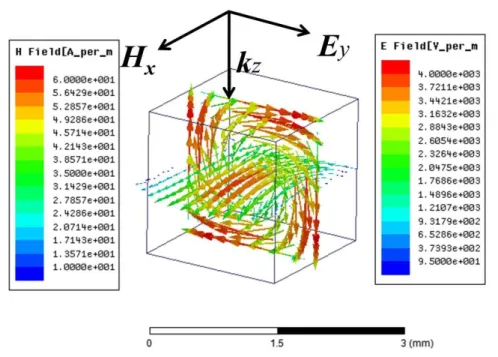
(30) Thèse de Jianping Hao, Lille 1, 2016 Chapter 1 Background and context. eff. 3f 1 1 F( ) 2bm V F( ) bm . F( ) . . 2(sin cos ) ( 1) sin cos 2. where be 1 2 , bm 1 2 ,V . 4 3. 1-4. 1-5. 3. r 0 , k 0r0 2 2 , V is the p. volume fraction of the spherical particles, r0 is the radius of the spherical particles, p is the lattice constant. F() is a resonant function and can be negative or positive at certain range of , which can provide negative permitivity and permeability.. Mie resonance applied in BST cube absorbers Turning now to the first Mie resonance in BST (BaxSr1-xTiO3) cubes with relavite permittivity r = 132, loss tangent tan= 0.025, respectively, it can be pointed out that the ground resonance is magnetic. This is shown in Fig. 1.1 that illustrates the confinement of the H field inside the cube while the electric field contours are wrapped along the H oriented symmetry axis. By means of this resonance, the surface impedance of the metamaterial absorber matches the free space impedance, thus minimizing the reflectance at the first Mie resonance mode around 11 GHz. At the same time putting a metallic plate on the bottom of the BST cube, which cuts off all the transmission waves, from the equation A = 1-R-T, one can have a unit absorption.. 9. © 2016 Tous droits réservés.. lilliad.univ-lille.fr.
(31) Thèse de Jianping Hao, Lille 1, 2016 Chapter 1 Background and context. Fig. 1.1 Electric (y-z plane) and magnetic (x-z plane) field distributions in a dielectric cube with sidewidth a = 1.8 mm at the first Mie resonance frequency 11.14 GHz.. 1.3.2 Plasmonic based perfect meta-material absorber Throughout the development of the PMA, the plasmonic resonant based PMAs have grown rapidly during the last decade due to the fact that they can possess broadband behaviors and other useful properties for real applications. Most of the PMAs are composed of three layers: (i) periodically metallic structured patterns, (ii) dielectric layer, (iii) continuous metallic plate [62]. The periodically-arranged metallic layers should be carefully designed to provide a certain resonance at the targeted frequency. Fulfilling the impedance matching condition to the free space is achieved by varying the dimensions of the resonators which can have various shapes such as ring, cross, patch, snowflake and so on. Under this impedance matching condition so that reflectivity on the device vanishes and all the incidence EM waves should be coupled to the device. The second dielectric layer plays a basic role by trapping the incident EM wave. At the resonant frequency of the absorber the EM waves are bouncing back and forth 10. © 2016 Tous droits réservés.. lilliad.univ-lille.fr.
(32) Thèse de Jianping Hao, Lille 1, 2016 Chapter 1 Background and context. inside the resonator so that the EM energy is dissipated efficiently. In other words the generic metal-dielectric-metal structure plays a role of resonant cavity with lifetime in the cavity related to frequency selectivity of the resonance through the quality factor. The primary role of the third metallic layer is to stop any transmission of the impinging wave. Also we will see in the following chapters devoted to plasmonic-type structures that the metallic regions facing the structured top metal layers support backside local currents flowing in the opposite direction to the top ones. To sum up when an electromagnetic wave is impinging on such a tri-layered medium, the fact that the transmission is zero and the reflection vanishes at the resonance means that all the EM energy is absorbed justifying the term of Perfect Metamaterial Absorber.. 1.4 Overview of the state of the art As aforementioned the first theoretical and experimental demonstration of PMA was reported by Landy et al.. For this work the absorber was composed of three layers [58] with two metallic patterns separated by a dielectric layer. The authors of this article demonstrated a simulated absorptivity near unity at 11.48 GHz [63]. Since this first demonstration, a large number of optimized PMA have been proposed addressing different frequency bands for different application areas. In this last section, a brief overview of the state of the art, summarized in table 1, is reported. While further details can be found in the reference listed in column 1, the second column gives some brief indications about the employed technology, D and M standing for full dielectric and metal respectively. Also the type of metal is specified. One can note that copper is currently used for microwave absorbers whereas the devices that operate in optics are often fabricated with silver or gold layers. The third column indicates the pattern type. When a pyramidal shape is specified this means the stacking of multilayered patches. In the subsequent columns are reported the central frequency (fc) corresponding generally to the maximum of absorbance and the fractional bandwidth (FB) which is defined by 11. © 2016 Tous droits réservés.. lilliad.univ-lille.fr.
(33) Thèse de Jianping Hao, Lille 1, 2016 Chapter 1 Background and context. using the FWHM frequency offset (f/fcFWHM). The last column gives some indications about sensitivity to the incidence angle () by considering an absorbance in excess of 90 %. Table 1 Overview of the state of the art of the broadband absorbers. Reference [63] D. Feng APL [64]. Q.. Liang. Advanced material [65] J. Yang Xplore. Technology. pattern. fc. f/fc. M-Cu. Pyramid. 9.75 GHz. 66.7 %. M-Cu. Pyramid. 7.5 m. 86.7 %. 4 GHz. 80 %. 10 m. 30 %. 12 GHz. 92 %. Independent angle. M-Cu M-Au. [66] Y. Cui, APL. D-Ge. Double square loop Nanoantennas Patch Crisscross. Angle sensitivity A > 90% = 40° A > 80% = 60° A > 90% = 45° A > 80% = 70°. [67] L. Sun, OE. M. [68] Q. Feng, OL. M-Ni. Cross. 32.5 THz. 107.7 %. A > 90% = 60°. [69] J. Grant, OL. M-Cu. Cross. 5 THz. 48 %. A > 90% = 80°. [70] C. Cheng, OE. M-Ag. Disk. 3.25 m. 24.6 %. A > 60% = 15°. [71] M. Li Xplore. M. Loop. 19.8 GHz. 92 %. A > 90% = 90°. M-Au. Split Ring. 205 THz. 150.1 %. A > 90% = 40°. M-Ag. Strip (taper). 550 nm. 79.6 %. A >90% = 70°. M-Cu. Split Ring. 0.5 THz. 79.6 %. M-. Patch (layers). 2.9 THz. 42.1 %. [72] K. B. Alici, OE [73]. K.. Aydin. Nature C. [74] N. R. Han, OE [75] B. X. Wang, IEEE Xplore [76] D. H. Kim, OE. D-Si. [77] C. Shi, APL. D-Si. [78] Z. Lu, JLT. M-Al. [79] J. Zhu, APL. M-Cr. [11] H. Xiong, APL. M-Cu. [80] D. Ji, Nature [81]. M.. Soheilifar,. Ring. Pyramid (flexible) Patch. FWHM: 1.23 THz 1.5 THz. 133.3 %. 0.8 m. 142 %. 1.7 THz. 135 %. 14.6 GHz. 102 %. array Split ring (layers). A > 90%:. Bent R = 2 cm. 125.2 %. triple-helix Patch (layers). A > 90% = 50°. A > 90% = 60°. A > 90% = 40°. Ag-SiO2. Taper (HMM). 4 m. 101 %. M-Cu. Split ring. 13.5 GHz. 111 %. A > 90% = 45°. Al–Si–Mg. Ring. 3.35 THz. 118 %. A > 90% = 90°. R. Int.. J.. Electron. Commun. [82] B. X. Wang,. 12. © 2016 Tous droits réservés.. lilliad.univ-lille.fr.
(34) Thèse de Jianping Hao, Lille 1, 2016 Chapter 1 Background and context. APE [83] Y. Yang, Nano Lett. [84] T. Cao, Science [85] B. Y. Wang, JAP [86] B. X. Wang, Phys. Scr. [87]. J.. Zhou,. Photonics. D-Si. Patch. 1550 nm. 20 %. = 90°. M-Au. Patch. 770 nm. 41 %. A > 80% = 80°. M-Ag. Patch. 12 GHz. 57.3 %. M-D. Two layers. 1.8 THz. 33 %. Au−Al2O3. Taper(HMM). 2 m. 75%. Tree Structure. 8.7 GHz. 87 %. A > 90% = 90°. Pyramid. 3 m. 186 %. A > 90% = 75°. A > 80% = 60°. [88] J. Ma, Prog. Electromagn.. Res.. Lett. [89] M. Lobet, OE. Cu-Ge. References [1] D. Shuring, J. J. Mock, B. J. Justice, S. A. Cummer, J. B. Pendry, A. F. Starr and D. R. Smith, Metamaterial electromagnetic cloak at microwave frequency, Science, Vol. 314, 977-980, 2006. [2] J. B. Pendry, D. Shuring and D. R. Smith, Controlling electromagnetic fields, Science, Vol. 312, 1780-1782, 2006. [3] D. Shuring, J. B. Pendry, D. R. Smith, Calculation of material properties and ray tracing in transformation media, Opt. Express, Vol. 14, 9794-9804, 2006. [4] M. Fridman, A. Farsi, Y. Okawachi and A. L. Gaeta, Demonstration of temporal cloaking, Nature, Vol. 481, 62-65, 2012. [5] D. P. Gaillot, C. Croenne and D. Lippens, An all-dielectric route for terahertz cloaking, Opt. Express, Vol. 16, 3986-3992, 2008. [6] R. Liu, C. Ji, J. J. Mock, J.Y. Chin, T. J. Cui and D. R. Smith, Broadband ground-plane cloak, Science, Vol. 323, 366-369, 2009. [7] J. B. Pendry, A. J. Holden, D. J. Robbins, and W. J. Stewart, Magnetism from Conductors, and Enhanced Non-Linear Phenomena, IEEE Trans. Microw. Theory 13. © 2016 Tous droits réservés.. lilliad.univ-lille.fr.
(35) Thèse de Jianping Hao, Lille 1, 2016 Chapter 1 Background and context. Tech., Vol.47, 2075-2084, 1999. [8] D. R. Smith, S. Schultz, P. Markoš, and C. M. Soukoulis, Determination of effective permittivity and permeability of metamaterials from reflection and transmission coefficients, Phys. Rev. B, 65, 195104, 2002. [9] R. A. Shelby, D. R. Smith and S. Schultz, Experimental verification of a negative index of refraction, Science 292, 77-79, 2001. [10] F. Capolino, Application of metamaterials, ISBN 978-1-4200-5423-1, 2009. [11] W. Adams, A. Vora, J. Gwamuri, J. Pearce and D. Güney, Controlling Optical Absorption in Metamaterial Absorbers for Plasmonic Solar Cells, Proc. of SPIE Vol. 9546, 2015. [12] S. Rudykh and Mary C. Boyce, Transforming wave propagation in layered media via instability-induced interfacial wrinkling, Phys. Rev. Lett., Vol. 112, 034301, 2014. [13] G. Singh, Rajni, A. Marwaha, A Review of Metamaterials and its Applications, IJETT, Vol.19, 2231-5381, 2015. [14] J. B. Pendry, Negative Refraction Makes a Perfect Lens, Phys. Rev. Lett., Vol. 85, 18, 2000. [15] W. Li and J. Valentine, Metamaterial Perfect Absorber Based Hot Electron Photodetection, Nano Lett., Vol. 14, 3510 - 3514, 2014. [16] A. Vora, J. Gwamuri, N. Pala, A. Kulkarni, J. Pearce and D. Güney, Exchanging Ohmic Losses in Metamaterial Absorbers with Useful Optical Absorption for Photovoltaics, Sci. Rep., Vol. 10, 1038, 2014. [17] B. Wu, W. Wang, J. Pacheco, X. Chen, T. Grzegorczyk and J. A. Kong, A study of using metamaterial as antenna substrate to enhance gain, PIER, Vol. 51, 295-328, 2005. 14. © 2016 Tous droits réservés.. lilliad.univ-lille.fr.
(36) Thèse de Jianping Hao, Lille 1, 2016 Chapter 1 Background and context. [18] S. Enoch, G. Tayeb, P. Sabouroux, N. Guerin and P. Vincent, A metamaterial for directive emission, Phys. Rev. Lett., Vol. 89, 213902, 2002. [19] W. W. Salisbury, Absorbent body for electromagnetic waves, US Patent, 2599 944, 1952. [20] W. H. Emerson, Electromagnetic wave absorbers and anechoic chambers through the years, IEEE Trans. Antennas Propag., Vol. 21, 484-490, 1973. [21] Y. Zhang, R. Mittra, B.-Z. Wang and N.-T. Huang, AMCs for ultra-thin and broadband RAM design, Electron. Lett., Vol. 45, 484-485, 2009. [23] A. Alù, and N. Engheta, Achieving transparency with plasmonic and metamaterial coatings, Phys. Rev. E, Vol.72, 016623, 2005. [24] J. B. Pendry, D. Schurig, D. R. Smith, Controlling electromagnetic fields, Science, Vol. 312, 1780-1782, 2006. [25] A. J. Ward and J. B. Pendry, Refraction and geometry in Maxwell’s equations, J. Mod. Opti., Vol. 43, 773-793, 1996. [26] D. Schurig, J. J. Mock, B. J. Justice, S. A. Cummer, J. B. Pendry, A. F. Starr, and D. R. Smith, Metamaterial Electromagnetic Cloak at Microwave Frequencies, Science, Vol. 314, 977-980, 2006. [27] A. Alù and N. Engheta, Cloaking and transparency for collections of particles with metamaterial and plasmonic covers, Opt. Express, Vol. 15, 7578-7590, 2007. [28] A. Alù and N. Engheta, Plasmonic materials in transparency and cloaking problems: mechanism, robustness, and physical insights, Opt. Express, Vol. 15, 3318-3332, 2007. [29] M. A. Antoniades, and G. V. Eleftheriades, Compact Linear Lead/Lag Metamaterial Phase Shifters for Broadband Applications, IEEE Antennas Wirel. 15. © 2016 Tous droits réservés.. lilliad.univ-lille.fr.
(37) Thèse de Jianping Hao, Lille 1, 2016 Chapter 1 Background and context. Propag. Lett., Vol. 2, 103-106, 2003. [30] E. L. Ginzton, W. R. Hewlett, J. H. Jasburg, and J. D. Noe, Distributed amplification, PIRE, Vol. 36, 956-969, 1948. [31] C. Caloz, F. P. Casares-Miranda, and C. Camacho-Penalosa, Active Metamaterial Structures and Antennas, IEEE MELECON, 268-271, 2006. [32] A. Grbic and G. V. Eleftheriades, A backward-wave antenna based on negative refractive index L-C networks, AP-S/URSI, Vol. 4, 340-343, 2002. [33] L. Lei, C. Caloz, and T. Itoh, Dominant mode leaky-wave antenna with backfire-to-endfire scanning capability, Electron. Lett., Vol. 38, 1414-1416, 2002. [34] A. Grbic and G. V. Eleftheriades, Experimental verification of backward wave radiation from a negative refractive index metamaterial, J. Appl. Phys., Vol. 92, 5930-5935, 2002. [35] J. R. James and P. S. Hall, Handbook of Microstrip Antennas. London, U.K. Peter Peregrinus, 1989. [36] M. Pozar and D. H. Schaubert, Microstrip Antennas: The Analysis and Design of Microstrip Antennas and Arrays, New York: IEEE Press, 1995. [37] S. Maci, G. Biffi Gentili, P. Piazzesi, and C. Salvador, Dual-band slot-loaded patch antenna, IEE Proc. Microw. Antennas Propag., Vol. 142, 225-232, 1995. [38] R. Porath, Theory of miniaturized shorting-post microstrip antennas, IEEE Trans. Antennas Propag., Vol. 48, 41-47, 2000. [39] A. Alù , F. Bilotti, N. Engheta, and L. Vegni, Subwavelength, Compact, Resonant Patch Antennas Loaded With Metamaterials, IEEE Trans. Antennas Propag., Vol. 55, 13-25, 2007. [40] V. G. Veselago, The electrodynamics of substances with simultaneously negative 16. © 2016 Tous droits réservés.. lilliad.univ-lille.fr.
(38) Thèse de Jianping Hao, Lille 1, 2016 Chapter 1 Background and context. values of and , Sov. Phys. Usp., Vol. 10, 509, 1968. [41] D. R. Smith, W. J. Padilla, D. C. Vier, S. C. Nemat-Nasser and S. Schultz, Composite Medium with Simultaneously Negative Permeability and Permittivity, Phys. Rev. Lett., Vol.84, 4184, 2000. [42] J. B. Pendry, A. J. Holden, D. J. Robbins and W. J. Stewart, Magnetism from Conductors, and Enhanced Non-Linear Phenomena, IEEE Trans. Microwave Theory Tech. Vol.47, 2075, 1999. [43] J. B. Pendry, A. J. Holden, W. J. Stewart and I. Youngs, Extremely Low Frequency Plasmons in Metallic Mesostructures, Phys. Rev. Lett., Vol. 76, 4773, 1996. [44] C.L. Holloway , E.F. Kuester, J. Baker-Jarvis and P. Kabos, A double negative (DNG) composite medium composed of magnetodielectric spherical particles embedded in a matrix, IEEE Trans. Antennas Propag., Vol. 51, 2596-2603, 2003. [45] B. Seo, T. Ueda, T.Itoh and H. Fetterman, Isotropic left handed material at optical frequency with dielectric spheres embedded in negative permittivity medium, Appl. Phys. Lett., Vol. 88, 161122, 2006. [46] A. Rennings, C. Caloz and I. Wolff, A Novel Clustered Dielectric Cubes Metamaterial (CDC-MTM), IEEE AP-S/URSI, 483-486, 2006. [47] J. D. Shumpert, W. J. Chappell and L.P. B. Katehi, Parallel-plate mode reduction in conductor-backed slots using electromagnetic bandgap substrates, IEEE Trans. Microw. Theory Tech., Vol. 47, 2099-2104, 1999. [48] J. B. Pendry, L. Martin-Moreno and F. J. Garcia-Vidal, Mimicking surface plasmons with structured surface, Science, Vol. 305, 847-848, 2004. [49] J. D. Baena, J. Bonache, F. Martín, R. M. Sillero, F. Falcone, T. Lopetegi, M. A. G. Laso, J. García–García, I. Gil, M. F. Portillo and M. Sorolla, 17. © 2016 Tous droits réservés.. lilliad.univ-lille.fr.
(39) Thèse de Jianping Hao, Lille 1, 2016 Chapter 1 Background and context. Equivalent-circuit models for split-ring resonators and complementary split-ring resonators coupled to planar transmission lines, IEEE Trans. Microw. Theory Tech., Vol. 53, 1451-1461, 2005. [50] C. Caloz, H. Okabe, T. Iwai, and T. Itoh, Transmission line approach of left-handed (LH) materials, IEEE AP-S/URSI., Vol. 1, 39, 2002. [51] G. V. Eleftheriades, A. K. Iyer and P. C. Kremer, Planar negative refractive index media using periodically L-C loaded transmission lines, IEEE Trans. Microw. Theory Tech., Vol. 50, 2702-2712, 2002. [52] A. Grbic and G. V. Eleftheriades, Periodic analysis of a 2-D negative refractive index transmission line structure, IEEE Trans. Antennas Propag., Vol. 51, 2604-2611, 2003. [53] C. Caloz, Dual composite right/left-handed (D-CRLH) transmission line metamaterial, IEEE Microw. Wirel. Compon. Lett., Vol. 16, 585-587, 2006. [54] S. Lim, C. Caloz and T. Itoh, Fellow, IEEE, Metamaterial-based electronically controlled transmission-line structure as a novel leaky-wave antenna with tunable radiation angle and beam width, IEEE Trans. Microw. Theory Tech., Vol. 52, 2678-2690, 2004. [55] R. S. Kshetrimayum, L. Zhu, Guided-wave characteristics of waveguide based periodic structures loaded with various FSS strip layers, IEEE Trans. Antennas Propag., Vol. 53, 120-124, 2005. [56] Q. Zhao, J. Zhou, F. Zhang, D. Lippens, Mie resonance-based dielectric metamaterials, Mater. Today, Vol. 12, 2009. [57] C. Vandenbem and J. Vigneron, Mie resonances of dielectric spheres in face-centered cubic photonic crystals, J. Opt. Soc. Am. A, Vol. 22, 1042-1047, 2005.. 18. © 2016 Tous droits réservés.. lilliad.univ-lille.fr.
(40) Thèse de Jianping Hao, Lille 1, 2016 Chapter 1 Background and context. [58] N. I. Landy, S. Sajuyigbe, J. J. Mock, D. R. Smith and W. J. Padilla, Perfect Metamaterial Absorber, Phys. Rev. Lett., Vol. 100, 207402, 2008. [59] Jackson, J. D., Classical Electrodynamics, 2nded., Wiley, New York, USA, 1999. [60] Zhao, Q., et al., Experimental Demonstration of Isotropic Negative Permeability in a Three-Dimensional Dielectric Composite, Phys. Rev. Lett., Vol. 101, 027402, 2008. [61] Q. Zhao, J. Zhou, F. Zhang, D.r Lippens, Mie resonance-based dielectric metamaterials, Mater. Today, Vol. 12, No 12, 2009. [62] C. M. Watts, X. Liu and W. J. Padilla, Metamaterial electromagnetic wave absorber, Adv. Mater., Vol. 24, 98-120, 2012. [63] F. Ding, Y. Cui, X. Ge, Y. Jin and S. He, Ultra-broadband microwave metamaterial absorber, Appl. Phys. Lett., Vol. 100, 103506, 2012. [64] Q. Liang, T. Wang, Z. Lu, Q. Sun, Y. Fum and W. Yu, Metamaterial-based Two Dimensional Plasmonic Subwavelength Structures Offer the Broadest Waveband Light Harvesting, Adv. Opti. Mater., Vol. 1, 43-49, 2013. [65] J. Yang and Z. Shen, A Thin and Broadband Absorber Using Double-Square Loops, IEEE Antennas Wirel. Propag. Lett., Vol. 6, 388-391, 2007 [66] Y. Cui, J. Xu, K. Fung, Y. Jin, A. Kumar, S. He, and N. X. Fang, A thin film broadband absorber based on multi-sized nanoantennas , Appl. Phys. Lett., Vol. 99, 253101, 2011. [67] L. Sun, H. Cheng, Y. Zhou and J. Wang, Broadband metamaterial absorber based on coupling resistive frequency selective surface, Opt. Express, Vol. 20, 4675 2012. [68] Q. Feng, M. Pu, C. Hu and X. Luo, Engineering the dispersion of metamaterial surface for broadband infrared absorption, Opt. Lett., Vol. 37, 2133, 2012. 19. © 2016 Tous droits réservés.. lilliad.univ-lille.fr.
(41) Thèse de Jianping Hao, Lille 1, 2016 Chapter 1 Background and context. [69] J. Grant, Y. Ma, S. Saha, A. Khalid and D R. S. Cumming, Polarization insensitive, broadband terahertz metamaterial absorber, Opt. Lett., Vol. 36, 3476, 2011. [70] C. Cheng, M. Abbas, C. Chiu, K. Lai, M. Shih and Y. Chang, Wide-angle polarization independent infrared broadband absorbers based on metallic multi-sized disk arrays, Opt. Express, Vol. 20, 10376, 2012. [71] M. Li, S. Xiao, Member IEEE, Y.Bai and B. Wang, Member, IEEE, An Ultrathin and Broadband Radar Absorber Using Resistive FSS, IEEE Antennas Wirel. Propag. Lett., Vol. 11, 748-751, 2012. [72] K. Alici, A. Turhan, C. Soukoulis and Ekmel Ozbay, Optically thin composite resonant absorber at the near-infrared band: a polarization independent and spectrally broadband configuration, Opt. Express, Vol. 19, 14260-14267, 2011. [73] K. Aydin, V. Ferry, R. Briggs and H. Atwater, Broadband polarization-independent resonant light absorption using ultrathin plasmonic super absorbers, Nat. Commun., Vol. 10, 1038, 2011. [74] N. R. Han, Z. C. Chen, C. S. Lim, B. Ng, and M. H. Hong, Broadband multi-layer terahertz metamaterials fabrication and characterization on flexible substrates, Opt. Express, Vol. 19, 6990-6998, 2011. [75] B. Wang, L. Wang, G. Wang, W. Huang, X. Li and X. Zhai, Theoretical Investigation of Broadband and Wide-Angle Terahertz Metamaterial Absorber, IEEE Photon. Technol. Lett., Vol. 26, 111-114, 2014. [76] D. Kim, D. Kim, S. Hwang and J. Jang, Surface relief structures for a flexible broadband terahertz absorber, Opt. Express, Vol. 20, 16815-16822, 2012. [77] C. Shi, X. Zang, Y. Wang, L. Chen, B. Cai and Y. Zhu, A polarization-independent broadband terahertz absorber, Appl. Phys. Lett., Vol. 105, 031104, 2014. [78] Z. Lu, M. Zhao, Z. Yang, L. Wu and P. Zhang, Helical Metamaterial Absorbers: 20. © 2016 Tous droits réservés.. lilliad.univ-lille.fr.
Figure


+7


Documents relatifs
In 2005 Hampton (2005) provides a new family of planar central con- figurations, called stacked central configuration, for the 5–body problem with an interesting property: the
It was found that the strength of field and near electrode voltage drop values increase with initial gas density [1, 2] and with increasing of current rate of rise
[r]
Le premier en prend les deux septièmes, le deuxième prend les deux cinquièmes du reste, le troisième prend les deux tiers du nouveau reste.. Il reste 6 bonbons dans
[r]
In order to find the appropriate parameters for which a plasmonic cavity can efficiently modify the electric and magnetic transitions of Eu 3+ nanocrystals, we first carried
Quand le numérateur est plus grand que le dénominateur il est supérieur à 1.. Quand le numérateur est plus petit que le dénominateur il est inférieur
FIGURE 5.8 The message created by entering an invalid telephone number in validator.html... Copyright © 2006
