UNIVERSITÉ DE MONTRÉAL
APPROACHING TYPICAL METALLIC CONDUCTIVITIES IN POLYMER NANOCOMPOSITES FOR LIGHTNING STRIKE PROTECTION
XAVIER CAUCHY
DÉPARTEMENT DE GÉNIE MÉCANIQUE ÉCOLE POLYTECHNIQUE DE MONTRÉAL
THÈSE PRÉSENTÉE EN VUE DE L’OBTENTION DU DIPLÔME DE PHILOSOPHIAE DOCTOR
(GÉNIE MÉCANIQUE) JUIN 2018
ÉCOLE POLYTECHNIQUE DE MONTRÉAL
Cette thèse intitulée :
APPROACHING TYPICAL METALLIC CONDUCTIVITIES IN POLYMER NANOCOMPOSITES FOR LIGHTNING STRIKE PROTECTION
présentée par : CAUCHY Xavier
en vue de l’obtention du diplôme de : Philosophiae Doctor a été dûment acceptée par le jury d’examen constitué de :
M. LÉVESQUE Martin, Ph. D., président
M. THERRIAULT Daniel, Ph. D., membre et directeur de recherche
Mme KLEMBERG-SAPIEHA Jolanta-Ewa, Ph. D., membre et codirectrice de recherche M. TAVARES Jason R, Ph. D., membre
DEDICATION
To you, Reason.
À Caroline, pour un soutien indéfectible,
À Adrien et Edmond, pour leurs rires et sourires,
À ma mère, pour la rigueur et le goût du travail bien fait,
À mon père, pour l’amour du débat,
À mes amis, pour les évasions,
ACKNOWLEDGEMENTS
I want to express my sincere gratitude to Prof. Daniel Therriault, my director, and prof. Jolanta-Ewa Klemberg-Sapieha, my co-director, for the priceless opportunity of pursuing a doctoral degree under their supervision. Their support and the discussions we had fueled me throughout this work. Many thanks also to all industrial members of the project: Mario Simard from Bombardier Aerospace, Judith Roberge and Michel Dion from Bell Helicopter and Larry Hebert from 3M. Many thanks to the organizations themselves for their participation in the project.
Thanks also to all my friends and colleagues from the Laboratory for Multi-Scale Mechanics (LM2) for the fruitful discussions and for the sheer joy of their companionship during these days of hard work: Anne-Marie Lanouette, Maxime Arguin, Nicolas Guérin, Renaud Passieux, Sampada Bodke, Rouhollah Farahani, Benjamin Le Dafniet, Qinghua Wu, Chao Xu, Kambiz Chizari.
A special thanks to Rajesh Ponnada, Hongqiu Wei and Martin Gagné for helping me with tasks related to the project.
Finally, I want to thank my friends and family for supporting me in times of need. A very special thanks to Caroline for her love and for yet another reason for lacking sleep: our two magnificent boys.
RÉSUMÉ
Parmi les objectifs de performance à atteindre lors de la conception d’un nouvel aéronef, la réduction de la masse de l’appareil est au premier rang, ladite masse ayant une influence directe sur les coûts variables de l’opération de l’aéronef. À cette fin, l’industrie a graduellement introduit les matériaux composites dans les composantes structurelles, desquelles le fuselage est peut-être la plus importante. La conversion du fuselage de l’aluminium aux matériaux composites n’est pas sans générer son lot de problèmes satellites. Notamment, la diminution de la conductivité électrique de la surface de l’appareil rend celui-ci vulnérable aux effets néfastes de la foudre.
En réaction à cette vulnérabilité, des grillages métalliques continus ont été ajoutés à la surface externe des panneaux composant le fuselage. Cet ajout augmentant considérablement la masse de l’ensemble sans contribuer à la rigidité, une demande pour des solutions alternatives fut créée. L’ajout graduel de charges conductrices à une matrice isolante donne lieu à une augmentation subite de la conductivité du composite et à une transition de l’état isolant à celui de conducteur à une concentration donnée, appelée le seuil de percolation. La recherche sur les composites de nanotubes de carbone a permis de mettre en évidence un seuil de percolation extrêmement bas pour les particules de haut rapport d’aspect. En réaction, de multiples études se sont succédé qui cherchèrent à repousser les limites de la conductivité électrique de tels matériaux. Malheureusement, leur performance est limitée par une importante résistance de contact à l’interface entre les particules au sein du composite.
Pour qu’un composite ait une conductivité électrique assez élevée pour canaliser l’énergie de la foudre, les charges utilisées devront être caractérisées simultanément par une faible résistance de contact, par une haute conductivité intrinsèque et par une propension à former un réseau connecté dans la matrice.
Une stratégie répondant à ces exigences consiste à forcer la percolation d’un réseau de charges métalliques par leur auto-organisation dans le composite. Dans cette optique, nous avons exploré la combinaison d’une dispersion aqueuse de colloïdes d’époxy et d’un précurseur liquide de l’argent, aussi à base aqueuse. Lors de l’évaporation des solvants, de l’argent atomique précipite préférentiellement dans la phase aqueuse qui forme une topologie connectée dans le volume du matériau. La stratégie permet d’atteindre un seuil de percolation extrêmement bas à 0.27 vol.%, alors que les charges d’argent parviennent typiquement à la percolation à une valeur autour de 20
vol.%. La conductivité atteinte est de 5400 S/cm pour une concentration de 12.3 vol.%, seulement un ordre de grandeur plus bas que si tout le métal participait au réseau. Malheureusement, des problèmes d’adaptation de la méthode aux matériaux standards des fabricants ont motivé une réorientation des efforts de recherche.
La deuxième stratégie poursuivie consiste à combiner les qualités des charges métalliques et des particules carbonées à haut rapport d’aspect en une charge hybride cœur-coquille composée de nanofibres de carbone enduites d’argent. La méthode est une version modifiée du procédé de Tollens pour la fabrication de miroirs adaptée à la métallisation de nanoparticules en suspension. Les étapes de la fonctionnalisation, de la sensibilisation et de la métallisation ont fait l’objet d’optimisations individuelles et des conditions préférentielles ont été identifiées pour chaque étape. Une couverture uniforme de toutes les particules a été réalisée, et la conductivité spécifique de dépôts de particules a été mesurée à 1.8 x 10³ S·cm2/g, soit environ un ordre de grandeur sous celle de l’argent pur.
Les travaux ont ensuite visé à adapter la technologie aux procédés existants en incorporant les charges développées à la surface d’un panneau de composite carbone-époxy standard de l’industrie aérospatiale. Les particules furent d’abord dispersées dans un solvant aqueux, puis filtrées au travers d’une membrane poreuse dans un procédé inspiré des méthodes de fabrication de papier. Le « papier » résultant de cette opération fut ensuite laminé sur un film d’époxy « B-staged » avant d’être infusé et collé simultanément à la surface du panneau de carbone-époxy en utilisant une méthode analogue à l’infusion assistée par vide. La conductivité de la couche ainsi obtenue fut mesurée à 2.5×10⁵ S/m. Cette valeur est analogue à celle des meilleurs adhésifs conducteurs à base d’argent, mais avec un taux de charge dix fois moindre. Les panneaux furent soumis à des tests d’émulation de la foudre correspondant à la limite supérieure des 35% des évènements les moins sévères avec succès.
Une solution complète de protection contre la foudre fut développée, de la synthèse de nanocharges sur mesure à l’inclusion de la solution à la surface de panneaux de carbone-époxy standards. Au-delà de l’application initiale, les nanocharges développées comportent des avantages potentiels pour des applications telles que les adhésifs conducteurs afin de minimiser le poids du produit, les coûts de matières premières ainsi que les performances en cyclage thermique. Le champ émergent
de la fabrication additive pourrait aussi bénéficier de la flexibilité accrue qu’apporte cette nouvelle solution.
ABSTRACT
Among all performance targets a new aircraft design seeks to achieve, reduction in weight is of primary importance since it has a direct influence on the energy costs. In pursuing this target, an increasing proportion of composite materials has been introduced into modern aircrafts’ structures. Perhaps the most important structural component, the fuselage has not been spared by change. Every change requires adjustment, and thus the problem of lightning strikes to aircraft has resurfaced as the conductive aluminum skin was replaced by a lower conductivity carbon fiber/polymer composite counterpart.
Bonding a continuous metallic mesh to the surface of the skin has solved the problem, only to see the quest for mass minimization resume as this additional metal along with its adhesive and matrix contributes to the weight without benefits on the structural front. A better technology is sought. Upon gradually incorporating conductive fillers in a non-conductive matrix, the material undergoes a sudden change from an insulator to a conductor at a concentration called the percolation threshold which differs for every matrix-filler combination and filler dispersion state. Research on carbon nanotubes composites has highlighted the ability of high aspect ratio fillers to reach percolation at a very low concentration. However, issues with contact resistance between individual particles inhibit the maximum performance such composites can historically reach.
If a polymer composite is to fulfill the requirements of lightning strike protection, the filler used should display simultaneously a high conductivity, a low contact resistance and a propensity to form connected networks through the matrix.
One strategy to obtain such a combination of properties is to force the percolation of metallic fillers through self-organization upon forming the composite. We explored such an avenue by combining an aqueous colloidal epoxy dispersion with a water-based silver precursor ink. Upon solvent evaporation, elemental silver precipitates preferentially in the continuous aqueous phase, effectively segregating the conductive phase in a connected topology and thus promoting the conductivity of the composite. A very low percolation threshold was achieved, at only 0.27 vol.%, whereas typical silver fillers percolation occurs around 20 vol. %. The conductivity achieved at 12.3 vol.% Ag is of 5400 S/cm, which is only one order of magnitude lower than if all silver participated fully to the network. Compatibility issues with the existing matrix systems however encouraged us to pursue another direction.
The second strategy investigated was to combine the qualities of metallic fillers and high aspect ratio carbonaceous particles in a hybrid core-shell silver-coated carbon nanofiber filler. We adapted the historical Tollens’ process for mirror silvering to a suspension of carbon nanofibers through optimization of every step: functionalization, sensitization and silvering. Preferred bath compositions for both the sensitization and silvering steps were identified. The resulting bulk nanoparticles displayed a specific conductivity of 1.8 x 10³ S·cm2/g, which is roughly one order of magnitude lower than that of pure silver.
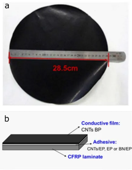
We then proceeded to devise a method for the incorporation of the developed filler particles to standard aerospace carbon fiber reinforced epoxy panels. The particles were put into dispersion before being filtered through a porous membrane in a process inspired from the papermaking body of knowledge. The nanoparticles were then transferred to a standard B-staged epoxy film commonly used as a surfacing film for composite fuselage panels. Next, the particles film was simultaneously bonded and infused by vacuum-assisted resin infusion on the surface of standard aerospace carbon fiber-epoxy provided by our industrial partners. The conductive layer thus obtained displayed a 2.5×10⁵ S/m value for conductivity, which is on par with class-leading silver-filled adhesives, but at a filler volume fraction a full order of magnitude lower. The panels were subjected to emulated lightning equivalent to the lesser 35% of the most severe lightning environment to which aircrafts are subjected with demonstrated protective effects.
A complete solution for lightning strike protection was developed, from the tailored synthesis of nanofillers to the inclusion in CFRP panels and lightning strike emulation. Apart from the initial targeted application for lightning strike protection, the developed nanoparticles have potential benefits for conductive adhesives in material costs, weight and thermal cycling resistance. The emerging field of additive manufacturing also stands to benefit from the added flexibility the technology developed provides.
TABLE OF CONTENTS
DEDICATION ... III ACKNOWLEDGEMENTS ... IV RÉSUMÉ ... V ABSTRACT ... VIII TABLE OF CONTENTS ... X LIST OF TABLES ... XIV LIST OF FIGURES ... XV LIST OF SYMBOLS AND ABBREVIATIONS ... XXII LIST OF APPENDICES ... XXIIIINTRODUCTION ... 1
CRITICAL LITERATURE REVIEW ... 4
2.1 Lightning strikes to aircraft ... 4
2.1.1 Strike mechanism ... 4
2.1.2 Direct effects of lightning strikes on carbon composite structures ... 9
2.1.3 Indirect effects of lightning strikes ... 10
2.2 Standards ... 11
2.2.1 Aircraft lightning zoning [17] ... 11
2.2.2 Standardized waveforms and lightning environment [19] ... 12
2.3 Lightning strike protection technology ... 14
2.3.1 Metal meshes ... 14
2.3.2 Alternative commercial solutions. ... 16
2.4 On the influence of layup on LSP performance ... 17
2.5.1 Carbon nanotubes ... 19 2.5.2 Carbon nanofibers ... 27 2.5.3 Graphene ... 28 2.5.4 Metallic fillers ... 29 2.5.5 Hybrid fillers ... 37 2.5.6 Summary ... 38
RESEARCH OBJECTIVES AND COHERENCE OF ARTICLES ... 40
3.1 Research objectives ... 40
3.1.1 Specific objectives ... 40
3.2 Presentation of the articles and articulation within the research objectives ... 41
ARTICLE 1: HIGHLY CONDUCTIVE HETEROGENEOUS EPOXY-SILVER COMPOSITES BY PHASE SELECTIVE IN-SITU FILLER SYNTHESIS. ... 43
4.1 Abstract ... 43
4.2 Introduction ... 44
4.3 Experimental ... 45
4.3.1 Silver ink preparation ... 45
4.3.2 PSFS-SEC samples preparation ... 46
4.3.3 Conductivity measurements ... 46
4.4 Microscopy ... 47
4.5 Results and discussion ... 47
4.5.1 Microstructural characterization ... 47
4.6 Electrical characterization ... 50
4.7 Conclusion ... 54
ARTICLE 2: SYNTHESIS OF HIGHLY CONDUCTIVE, UNIFORMLY
SILVER-COATED CARBON NANOFIBERS BY ELECTROLESS DEPOSITION. ... 56
5.1 Abstract ... 56 5.2 Introduction ... 57 5.3 Experimental section ... 59 5.3.1 Functionalization ... 59 5.3.2 Sensitization ... 59 5.3.3 Tollen’s Reagent ... 60 5.3.4 Reducing solution ... 60 5.3.5 Reaction ... 60 5.3.6 Characterization ... 60
5.4 Results and discussion ... 61
5.4.1 Starting Material and functionalization ... 61
5.4.2 Sensitization ... 67
5.4.3 Silver Deposition ... 74
5.5 Conclusion ... 82
5.6 Supporting information ... 83
5.6.1 Electroless silver deposition reaction ... 83
5.6.2 Nanoparticles packing ... 84
5.6.3 Oxidation ... 85
ARTICLE 3: HYBRID CARBON-SILVER NANOFILLERS FOR COMPOSITE COATINGS WITH NEAR METALLIC ELECTRICAL CONDUCTIVITY. ... 88
6.1 Abstract ... 88
6.2 Introduction ... 88
6.3.1 Conclusion ... 102 6.4 Experimental Section ... 102 6.4.1 Functionalisation : ... 102 6.4.2 Sensitization : ... 103 6.4.3 Solutions preparation : ... 103 6.4.4 Silver deposition : ... 103 6.4.5 Conductivity measurements : ... 104 6.4.6 Imaging : ... 104 6.4.7 Coating fabrication : ... 104
6.4.8 Lightning strike emulation : ... 105
6.4.9 Ultrasonic inspection : ... 105
6.5 Supporting Information ... 105
6.5.1 Choice of template particles ... 105
6.5.2 Deposition rate ... 106
DISCUSSION ... 108
CONCLUSION AND RECOMMENDATIONS ... 111
8.1 Conclusion ... 111
8.2 Recommendations ... 115
BIBLIOGRAPHY ... 118
LIST OF TABLES
Table 2.1: Peak currents and action integrals for cloud-to-ground flashes [19] ... 9 Table 2.2: Electrical performance of SWCNT and MWCNT buckypapers ... 24 Table 2.3: Summary of prospective strategies for next generation LSP systems ... 39 Table 4.1: Experimental resistivity values for PSFS-SEC samples with various silver loadings .. 51 Table 5.1: Oxygen at. % on CNF surface for different treatment conditions ... 64 Table A.1: Summary of available LSP systems ... 137 Table B.1: Taguchi matrix for initial experiments ... 140
LIST OF FIGURES
Figure 2.1: Intercepted (above) vs triggered (below) processes for lightning strike to aircraft. Also shown in the figure is the lightning propagation according to the bidirectional leader theory. Reproduced from [1] ... 5 Figure 2.2: Aircraft-initiated lightning strike on takeoff. Leaders expanding away from plane can
be clearly seen [16] ... 7 Figure 2.3: Illustration of the lightning channel reattachment process. Ec is the critical breakdown
electric field and Vinf is the relative speed of the plane to the viscous media [18] ... 8 Figure 2.4: Schematic of a natural current waveform during a lightning strike [2] ... 8 Figure 2.5: Typical lightning strike emulation damage to unprotected CFRP panel [10]. Fiber
shortening is observed at the attachment point as well as lifted plies in the fiber direction. Resin blistering and swelling is also observed ... 10 Figure 2.6: Lightning strike zoning per ARP5414 [17]. Adapted from [21] ... 12 Figure 2.7: Standardized current test waveform per [19]. Component A represents the first return
stroke and applies only to Zone 1 areas ... 13 Figure 2.8: Expanded metal meshes. a) Fabrication method where a die cuts openings in a metal
foil. The foil is then expanded in the direction indicated by the arrow [8]. b) Picture of an expanded copper mesh [25]. c) Fabrication parameters, SWD: short way of the diamond. LWD: long way of the diamond [25]. d) Typical stacking of layers on a composite panel [8] ... 15 Figure 2.9: Areal weight of different commercial expanded metal mesh LSP prepregs along with
the corresponding calculated specific conductivity [26, 27] ... 16 Figure 2.10: Disposition of the different layers in the prospective LSP system investigated by Han
et al. a) As-produced buckypaper. b) Layer structure of LSP system. Reproduced from [35] ... 18 Figure 2.11: Basis vectors of graphene crystal structure. The chiral vector of a SWCNT is expressed
as a linear combination of the basis vectors a1 and a2 ... 20 Figure 2.12: Fiber spinning from nanotubes "forest"[74] ... 26
Figure 2.13: HR-TEM image of a CNF sidewall. The inset is a conceptualization of the stacked-cup structure [72] ... 27 Figure 2.14: Optical micrograph of a 2.91 wt % ITO PMMA composite. Concentration of ITO at
the grain edges appear as darker lines on the image [98] ... 30 Figure 2.15: Migration of atoms through evaporation/condensation during sintering. Reproduced
from [100] ... 32 Figure 2.16: Melting temperature of Cu and Ag nanoparticles as a function of their diameter .... 32 Figure 2.17: Neck formation at the junction of two particles ... 34 Figure 2.18: SEM micrography of silver nanoparticles sintering by microwave radiation. a) the
unsintered particle layer before microwave irradiation. b) the resulting product after microwave radiation exposure. Reproduced from [108] ... 35 Figure 2.19: Plasmonic welding of Ag nanowires. a) TEM image of a nanowire junction prior to
IPL exposition. b, c) TEM images of junctions after IPL exposition. d) High resolution TEM image of the junction depicted in c) outlining the change in crystal orientation at the junction. Reproduced from [111] ... 36 Figure 2.20: TEM images of a) pristine and b) silver coated CNTs obtained by Tollen's process.
The poor focus in a) and the decrease in diameter after deposition do not allow to conclude that the MWCNTs are indeed uniformly coated with silver ... 38 Figure 4.1: a) Representative optical microscope image of the EPI-REZ 5522-WY-55 epoxy
emulsion. b) Size distribution of epoxy solids colloids within the emulsion. The mean size is 0.98 µm and the modal value lies within the [0.6, 0.66] µm interval. The measurements were performed on image a) ... 48 Figure 4.2: Optical microscope image of an epoxy emulsion-silver ink sample with 4.4 vol.% silver
content. The epoxy phase is lit by light transmission while the silver-rich phase is lit with reflected fluorescent lighting ... 49 Figure 4.3: SEM images of the cured epoxy-silver composite in low angle backscattered electron
imaging. Silver appears bright while epoxy is dark and transparent ... 50 Figure 4.4: Current-voltage curves for PSFS-SEC samples of various silver loadings ... 51
Figure 4.5: Evolution of the PSFS-SEC’s resistivity with silver volume content the green dotted line is the best fit of the percolation power law ... 53 Figure 5.1: As-received CNFs characterization. a) Schematics of the CNF graphitic planes
structure. b) TEM image showing the concentric and stacked cup regions of a typical CNF (scale bar 50 nm). c) TEM image showing the high aspect ratio of the CNFs both bamboo shaped and concentric-stacked cup type (scale bar 1 µm). d) A close-up of a bamboo shaped CNF. The graphitic planes configuration is clearly visible (scale bar 100 nm). e) XPS survey of pristine CNFs. Only the carbon peak is visible. The inset shows a high resolution spectrum of the carbon C1s peak. It shows only graphitic carbon, with the corresponding bonding-anti bonding peak ... 63 Figure 5.2: Functionalized CNFs characterization. a) TEM image showing that the aspect ratio
(~100) is preserved through functionalization (scale bar 1µm). b) TEM showing lifted graphitic planes at the nanofiber surface. This is the type of damage that can be found on ultrasonically assisted acid functionalization of CNFs (scale bar 100 nm). c) XPS high resolution spectrum of the O1s peak created by functionalization. The bonds are consistent with carboxylic functional groups. d) High resolution spectrum of the C1s peak. The importance of O–C=O relative to C–O and C=O bonds show a slight prevalence of carboxylic acid groups. Many new bonds are formed compared to pristine CNFs (Figure 5.1-e) ... 66 Figure 5.3: Contact angle measurements on CNF buckypapers. a) pristine CNF buckypaper. b)
Acid functionalized buckypaper ... 67 Figure 5.4: Sedimentation behavior and Zeta potential for sensitized CNFs. HCL concentration
doubles in each sample, from 20 mM (#1) to 640 mM (#6). a) Particles in the SnCl2 solution at the end of the sonication process. CNFs do not disperse in the 320 and 640 mM solutions. b) Rinsed particles in deionized water. No ultrasonic power was applied for dispersion. The sample with 640 mM HCl does not disperse spontaneously. c) Same as b), with 10 min. ultrasonic agitation and 90 hours sedimentation. The settling time increases with concentration until 320 mM (sample 5). d) Zeta potential of the dispersions in c) diluted to 10 times their volume. No significant variation was measured ... 69 Figure 5.5: Representative TEM images of sensitized CNFs. a) Sensitized with 60 mM HCl. Large
solution. The distribution of tin particles is uniform and amounts to roughly 1.5×10⁵ particles/µm2. The inset shows the crystal plane distance of 3.4 Å, which is consistent with SnO2 (scale bar 5 nm) ... 72 Figure 5.6: High resolution XPS spectra of tin-sensitized CNFs. a) Shows the tin peak with the
usual 1.5 ratio between Sn3d3/2 and Sn3d5/2 peak areas. The Sn3d5/2 peak is found at 487.5 eV. b) Sn Auger peaks. The kinetic energy of the Sn M4N45N45 is found at 431.7 eV and adds to the Sn3d5/2 energy for an Auger parameter of 919.2, which indicates that tin is under the Sn(IV) oxidation state. c) Oxygen 1s peak. The Sn-OX stoichiometry further confirms that tin is tetravalent ... 73 Figure 5.7: Electrical properties of hybrid nanoparticles as a function of silver to dextrose molar
ratio. a) A linear trend appears in sample mass (●) while the electrical conductivity (ᴏ) undergoes a sudden change at 0.8 molar ratio. b) Specific conductivity (◊) of the samples . 75 Figure 5.8: SEM images of samples with different Tollens’ reagent contents. a) bulk view of sample
at molar ratio 0.65. The coating is disconnected, and large isolated silver aggregates are visible (scale bar 1 µm). b) close-up of a large silver crystal at 0.65 molar ratio (scale bar 500 nm). c) Bulk view of sample at molar ratio 0.81. The coating morphology suddenly transitioned from disconnected to mostly connected and uniform. No large aggregates are visible (scale bar 1 µm). d) Close-up of the silver coating at 0.81 molar ratio. Silver deposits are connected but some bare patches are visible (scale bar 1 µm). e) Bulk view of sample at 1.14 molar ratio corresponding to the maximum specific conductivity. All fibers are coated evenly and no large aggregates are visible (scale bar 5 µm). f) Close-up view of sample at 1.14 molar ratio. No bare carbon patches are visible (scale bar 1 µm). g)-h) Sample at 1.47 molar ratio. The coating is uniform, and no bare patches are visible, but large aggregates are visible (scale bars 1 µm and 500 nm, respectively). The coating becomes continuous somewhere around 0.8 molar ratio ... 77 Figure 5.9: Electrical properties with respect to dextrose to silver molar ratio. a) Mass (●)and sheet
conductivity (○). The mass of samples stays fairly constant over the 0.5 molar ratio, consistent with a stoichiometric concentration of dextrose. As dextrose is in excess, the sample mass stays constant. b) Specific conductivity (◊). The values remain mostly constant for glucose in
excess. The inset provides the same values on a linear scale for comparison with Figure 5.7 ... 79 Figure 5.10: SEM images of samples with different dextrose concentrations. a) and b) Sample #2.
Silver metal forms in disconnected 100-500 nm thick islands. Scale bars are a) 1 µm and b) 500 nm. c) Bulk view of sample #4. All fibers are coated and the silver is connected. Scale bar is 5 µm. d) close-up view of a fiber from sample 4. Some bare patches of carbon are visible. Scale bar is 1 µm. e) and f) Sample #6. All fibers are uniformly coated. No bare patches are visible. Scale bars are e) 5µm and f) 1 µm ... 81 Figure 5.11: Optical microscope image of the cross section of the highest specific conductivity
sample with a Ag/dextrose molar ratio of 1.14. The average thickness of the nanoparticle film is 127 µm for a density of 0.4 g/cm3 ... 85 Figure 5.12: A photograph of samples produced during experiments on a) dextrose concentration
variation and b) Tollen’s reagent amount variation. The color bars show the average color picked on the samples images ... 86 Figure 5.13: The edge o nanoparticles after drying. The region under the ridge of the funnel (a)
shows a lighter color than the bulk of the sample (b) ... 87 Figure 6.1: Steps in the Ag deposition process. The top images are conceptual representations of
the CNF status at each step. a) Pristine CNF as imaged with TEM. The CNFs consist of a stacked cones graphitic structure core and a concentric cylindrical structured exterior surface (scale bar 20 nm). b) Sn covered CNF. Small nanocrystals 3-5 nm in size cover the whole surface of the CNF. The core structure is shadowed (scale bar 100 nm). c) Initial Ag deposits after 70 seconds reaction time. Small Ag nanoparticles are initiated on the surface of the CNF. Most of the carbon is still exposed. The thickness of the deposits is approximately 50 nm (scale bar 200 nm). d) Percolation of the Ag deposits after 170 seconds. An interconnected Ag islands path starts to develop along most CNFs. Deposits thickness is still approximately 50 nm (scale bar 300 nm). e) After 580 seconds deposition. The whole CNF surface is covered with silver (scale bar 300 nm) ... 92 Figure 6.2: Detailed view of a representative Sn layer. a) Overall TEM view of the side of a CNF
after Sn sensitization treatment. Most of the CNF structure is shadowed by Sn deposits. Some areas remain where the graphitic planes of the CNF can be seen (scale bar 20 nm). b) Close
up of the same CNF. The imaged zone is framed in red in a). The size of individual crystals can be estimated by measuring the diameter of zones exhibiting parallel planes (red circles). Sizes are 3-5 nm (scale bar 5 nm) ... 93 Figure 6.3: Ag coating evolution during time. a) Sample weight evolution during deposition time.
Error bars represent the standard deviation of a set of volume measurements performed with the equipment used in the experiment. A good fit is obtained with the behaviour postulated in equation (1). The deposition rate evolution is computed from the fit. b) Electrical conductivity () and specific conductivity () of samples. The error bars on the conductivity values represent the standard deviation on the set of 15 measurements performed on each sample. The conductivity evolution suggests two different regimes which are confirmed by the specific conductivity behaviour ... 95 Figure 6.4: Ag-CNFs morphology. a) Close-up view of an Ag-CNF after 30 min deposition. Tightly
packed individual crystallites are visible (scale bar =300 nm). b) View of bulk Ag-CNFs after 15 min deposition. The individual particles maintained a length of the order of 10 µm (scale bar = 1 µm) ... 97 Figure 6.5: Coating fabrication process schematic. a) The nanoparticles dispersion is poured in the
filter apparatus. b) After vacuum is applied, particles form a uniform layer on the filter membrane. c) The filter membrane is removed from the apparatus and left to dry. d) The filter membrane bearing the dried particles is pressed against a b-staged epoxy film fitted on a CFRP plate. The particles are transferred to the epoxy film. e) After vacuum assisted resin infusion and curing at 150 °C, the nanoparticles are embedded on the CFRP plate surface. f) Photograph of a cut-out from a panel prepared as described above. The sample thickness is 1.8 mm. g) Cross-sectional view of the same sample as in f) showing the conductive layer compared to the panel thickness. The hybrid nanofiber layer shows in a yellowish silver color (Scale bar = 500 µm). g) A close-up of the cross section that was used to measure the nanofibers-filled region thickness. The gray region is the surfacing film without conductive fillers (Scale bar = 100µm) ... 98 Figure 6.6: Lightning strike simulation. a) The current waveform generated by the simulator, with
a peak current of 15 kA and an action integral of 2650 A2s b) A photograph showing the whole surface of the nanocomposite protected CFRP panel. Scale bar = 5 cm. c) An angled
photograph of the surface showing the absence of lifted plies. Scale bar = 1 cm. d) A photograph of an unprotected CFRP panel subjected to the same current discharge as in a). Scale bar = 1 cm. e) C-scan of the nanocomposite protected CFRP panel surface showing no damage. Scale bar = 50 mm. The color scale units are µm. f) C-scan of the unprotected CFRP panel surface showing significant damage. The area around the leader attachment point is slightly swelled and the strike zone shows damage to the composite. Scale bar = 50 mm. The color scale units are µm ... 101 Figure 6.7: SEM image of crystallite size upon initial silver deposition after 72 s reaction time. The
smallest measurable silver particle dimension is ~22 nm. The scale bar = 100 nm ... 106 Figure 6.8: Reaction vessel color evolution. In the first minute of reaction, the glass takes a yellow
tint that slowly turns to a reddish brown. The glassware becomes opaque to the naked eye at the 10th minute ... 107 Figure B.1: Early electroless deposition experiment with formaldehyde as a reducing agent .... 139 Figure B.2: Sample 3 from the Taguchi matrix ... 140
LIST OF SYMBOLS AND ABBREVIATIONS
BMI ... BisMaleImide CNF ... Carbon NanoFiber. CNT ... Carbon NanoTube.
CFRP ... Carbon Fiber Reinforced Polymer. Ec ... Critical breakdown electric field
GO/rGO ... Graphene Oxide/reduced Graphene Oxide IPL ... Intense Pulsed Light
ITO ... Indium Tin Oxide
LSP ... Lightning Strike Protection. LWD ... Long Way of the Diamond. PAA ... Poly(Acrylic Acid).
PEN ... PolyEthylene Naphtalate PMMA ... Poly(Methyl MethAcrylate)
PSFS-SEC ... Phase Selective Filler Synthesis Silver-Epoxy Composite. PVDF ... PolyVinyliDene Fluoride
PVP ... PolyVinylPyrrolidone.
SEM ... Scanning Electron Microscope. SWD ... Short Way of the Diamond.
TEM ... Transmission Electron Microscope. XPS ... X-ray Photoelectron Spectroscopy.
LIST OF APPENDICES
APPENDIX A – LOOKUP TABLE FOR COMMERCIAL LSP SYSTEMS ... 137 APPENDIX B – ADDITIONAL ABSERVATIONS ... 138
INTRODUCTION
Managing the immense energy conveyed by a lightning strike has always been a subject of concern for aircraft design. Although being struck by lightning is often seen as an unpredictable and very rare event, such is not the case with aircrafts as theory, experiments and available data point out that the very presence of a craft in the electric field generated in the vicinity of a thunderstorm creates a concentration of the field that initiates the electrical breakdown of the atmosphere and therefore initiates the lightning discharge [1, 2]. Accordingly, each commercial aircraft has a probability of being struck by lightning of approximately once every year [1].
In early wooden aircraft, the effects of lightning strikes were often catastrophic as the nonconductive materials used in the structure were unable to handle such large amounts of electrical energy. Catastrophic failures largely declined with the advent of metallic aircrafts [3] since current would flow freely through the fuselage. The problem has however resurfaced with the increasing utilization of polymer matrix composites in aircraft structures.
The industry had to palliate the low conductivity of polymer composites by resorting to metallic meshes that are bonded to the aircraft skin. This solution is a compromise: while adding conductivity, it also adds non-structural weight which impairs the strength to weight ratio that initially justified the added complexity of using composite materials. Moreover, these meshes add to the complexity of the manufacturing process and are difficult to repair. A better solution is sought.
Recent advances in micro and nanomaterials and microfabrication have paved the way for research efforts in tailoring the properties of composite materials to meet specific targets. Composites with self-healing abilities [4], enhanced out-of-plane properties [5], energy storage [6] and electrical conductivity [7]. Among these, the latter is of prime interest to the problem at hand. Electrical conductivity is imparted to polymeric composites by establishing a connected network of conductive fillers within the matrix. Carbon nanotubes are often the preferred nanofillers to accomplish this task [7]. However, the reader will be presented with other alternatives in Section 2.5 as potential replacement technologies for lightning strike protection (LSP) are discussed. The proposed approach to this research was to investigate different fillers in resin systems compatible with aerospace requirements and to perform an initial assessment of the performance
upon which a filler would be chosen to investigate further. Optimisation work was then undertaken on this chosen research avenue. Next, the technology was adapted to aerospace standard carbon fibre reinforced polymer (CFRP) to provide a conductive coating, and the technology was tested in an emulated lightning environment. The research took place within the CRIAQ framework in a multi-disciplinary partnership with McGill University, UQAM and École Polytechnique de Montréal. The industrial partners were Bombardier Aerospace, Bell Helicopter Textron and 3M. The research avenues of the different teams were: graphene and its composites (UQAM), cold spray coatings (McGill), conductive nanocomposites (École Polytechnique de Montréal) and lightning emulation and materials testing (École Polytechnique de Montréal). This research fulfils the “conductive nanocomposites" part of the project.
Before a solution could be put to test through lightning strike emulation, initial assessment of the different solutions had to be performed. Therefore, although the performance of a solution is multi-factorial, a key measurable quantity had to be identified. We chose to examine the specific conductivity of the material as the main figure of merit as it expresses the ability of a material to transport charges per unit mass, two competing issues fundamental to the problem at hand.
The thesis is organized around articles submitted or published in peer-reviewed literature. The articles are presented in a logical order: the first paper in Chapter 4 presents early efforts to develop a coating with conductive fillers synthesised in-situ in a segregated, forced percolation network. The technology yielded excellent specific conductivity values but was not pursued because of manufacturing-related issues. The work was nonetheless published in peer-reviewed conference proceedings and is presented herein. It is our opinion that more work on this technology might be of value.
Following the early efforts, the focus of the research shifted to hybrid nanoparticles. The steps to achieve the hybrid silver coating-carbon core high aspect ratio nanofillers were investigated in-depth and reported in terms of the specific conductivity in the second article, published in a ACS Applied Materials and Interfaces, which the reader will find in Chapter 5.
Following the development of the nanofillers, the research energy shifted to the application of the technology for lightning strike protection of aircrafts. The third article presents the developed solution for the incorporation of the technology in CFRP panels in a robust manner, and with methods compatible with the existing materials and processes. Emulated lightning strikes were
performed on the panels produced and the results are reported. The paper, presented in Chapter 6, is currently under evaluation by a peer-reviewed journal.
CRITICAL LITERATURE REVIEW
This chapter describes the current state of knowledge concerning the phenomenon of lightning strikes to aircrafts. The first part is a review of the physical manifestations of lightning with emphasis on the particularities of aircraft-related incidents. The reader will find in the second part a description of current lightning strike protection systems along with a review of the research published both on new technologies for lightning strike protection systems and on potential technologies for future systems.
2.1 Lightning strikes to aircraft
A typical commercial plane will be subjected to a lightning strike once in every 1000 to 10,000 hours of flight [8] with an average around 3000 hours, or one strike pear service year [1]. Hence, preventing the detrimental effects of lightning on the structure and avionics of the aircraft is of primary importance for the users’ safety. These effects are classified between direct, defined as those which are observed at the lightning attachment points, and indirect effects, mainly caused by the stray currents and voltages induced by the electromagnetic fields generated during a lightning strike [2]. Typically, indirect effects will affect the onboard electronics and direct effects will cause puncturing of radomes, and melting of metal skins [2]. Composite structures are more vulnerable to direct effects because of their lower conductivity: Delamination as well as blistering, resin evaporation, fiber shortening and ply lifting are examples of the direct effects of lightning on these materials [9-12]. Sections 2.1.1, 2.1.2 and 2.1.3 provide an overview of the chain of events, from the inception of the lightning channel to the effects of the strike.
2.1.1 Strike mechanism
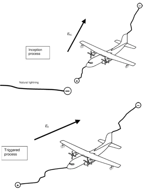
Aircraft-related lightning events can be divided between two categories: aircraft-intercepted discharge and aircraft-initiated discharge [1, 2, 13]. Figure 2.1 shows both mechanisms: In the upper half, an aircraft happens to be in the vicinity of a developing lightning channel. The second half shows a lightning channel developing from the aircraft itself and propagating in opposite directions. It has been shown in the 1980’s that the latter accounts for about 90% of total strikes, [1, 2] which explains the surprisingly high frequency of lightning strike events. The widely accepted explanation for the initiation of the lightning channel by the very presence of the aircraft
is called the “bidirectional leader” theory [2]. This theory stipulates that the dielectric breakdown of gases surrounding the aircraft initially occurs at two points on the aircraft’s surface and subsequently propagates according to the ambient electric field direction.
Figure 2.1: Intercepted (above) vs triggered (below) processes for lightning strike to aircraft. Also shown in the figure is the lightning propagation according to the bidirectional leader theory.
Reproduced from [1]
While an ambient electric field of the order of 50 kV/m as measured at the time of a lightning discharge is insufficient for breakdown [2, 13], Petrov et al. showed that a local increase in electric
field arises from polarization effects in the aircraft body: The field inside a conductor is always null because any field will act on charges until they reorganize in such a way that the field is exactly canceled. In pointed objects, this translates to a very high charge concentration at the extremities which adds to the existing field outside the conductor. This effect is responsible for providing the extra field strength necessary for breakdown [13]. Consistent with this theory, sharp extremities such as the radome and wing tips are the most frequent lightning attachment points [14]. Figure 2.2 shows a lightning strike to an aircraft on takeoff. A careful observer will notice faint elongated structures besides the main lightning channel that seem to originate from the aircraft and dissolve into the air. These structures are in fact lightning strikes in development, called secondary leaders. Since the leaders are seen to be expanding from the aircraft in both directions, the image is a very strong confirmation of the bidirectional leader theory as an intercepted lightning strike would have shown a leader expanding away from the aircraft in a single direction. Here again, the leaders are seen originating from points of high curvature on the plane, namely the radome and the wingtip, thus further supporting the theory.
The current waveform as measured on airplanes consist of two phases: the initiation phase and the sweeping phase [15]. The lightning channels are developed during the initiation phase, with a steady current of tens to hundreds of amperes (A) [2, 15]. Bursts of current that reach tens of kA are superimposed on the continuous component. The whole initiation phase takes place in a few milliseconds while bursts exhibit a duration of the order of the µs [2]. The time between bursts ranges from microseconds to milliseconds [2, 15].
Figure 2.2: Aircraft-initiated lightning strike on takeoff. Leaders expanding away from plane can be clearly seen [16]
The sweeping phase owes its name to the lightning channel sweeping the aircraft’s surface. While lightning channels are stationary on the event timescale and in the frame of reference of the earth, in frame of reference of the aircraft they are not [17]. Figure 2.3 illustrates the sweeping process in the aircraft reference frame. The ionized lightning channel suffers shear in the air flow boundary layer. Far from the aircraft’s surface the flow speed is Vinf, equal to the relative speed of the plane to the viscous media, while immediately on the surface the relative flow speed is 0. The plasma channel thus undergoes stretching. Combining this effect with the natural fluctuation of the plasma leader around its path causes certain points in the channel to approach the plane’s surface. When
the electric field between a point in the lightning channel and the aircraft’s surface reaches the critical breakdown value (Ec), a new channel is formed that is attached to a new, rearward position on the aircraft [1, 18]. Current intensity and duration are more important during the sweeping phase with bursts reaching a few tens of kA over a constant component of tens of A [2, 15]. The bursts are called return strokes and occur when the lightning channel closes the circuit between charged regions.
Figure 2.3: Illustration of the lightning channel reattachment process. Ec is the critical breakdown electric field and Vinf is the relative speed of the plane to the viscous media [18]
Figure 2.4 represents a typical case of lightning strike to aircraft. The intensity is scalable to represent more severe cases. The initiation phase can be seen with sharp bursts of current, followed by the sweeping phase with intense pulses of current. These pulses can occur even after the constant current component has extinguished.
The aircraft-related data presented in the literature mainly originates from intra-cloud flashes which occur between regions of different polarity within the same cloud. While being more frequent, these flashes are less severe than cloud-to-ground flashes. The peak current as measured at ground level during cloud to ground strikes is presented in Table 2.1 [19] along with the integral of the current squared over time (action integral), which provides a measure of the energy dissipated in the struck medium.
Table 2.1: Peak currents and action integrals for cloud-to-ground flashes [19]
Flash type Peak current, highest 50% threshold (kA)
Peak current, highest 5% threshold (kA) Action integral, highest 5% threshold (A2s) Negative 30 80 5.5×10⁵ Positive 35 250 1.5×10⁷
A negative flash carries negative charge from the cloud to the ground while a positive one removes negative charge from the ground. Negative flashes account for 90% of cloud-to-ground flashes [19]. Although the occurrence of an aircraft being struck by a positive strike is scarce, they must be taken into considerations when designing protection systems.
2.1.2 Direct effects of lightning strikes on carbon composite structures
These effects directly arise from the attachment of lightning channels and subsequent propagation of the lightning current in the material. Many factors contribute to the overall damage resulting from a lightning strike [18]. Thermal effects include the heat flux from the lightning plasma channel as well as joule heating from the current propagation. Mechanical effects arise from the lightning channel explosion shockwave, from overpressure induced by magnetic forces acting on the plasma channel, from magnetic pressure arising from the current flowing in the structure and from stresses induced by the rapid thermal expansion of the material [18].
For carbon structures, another form of damage arises from the electrical breakdown of the insulating matrix between adjacent plies [18]. Figure 2.5 provides an image of the typical damage inflicted to unprotected carbon fiber reinforced plastic (CFRP) panels. The damage observed on unprotected panels includes fiber shortening and resin vaporization at the arc attachment point,
lifting of the ply on a strip shaped geometry in the direction of the fiber and resin blistering around the attachment point [10, 12].
Feraboli et al. [12] performed lightning strike emulations on both unnotched and filled-hole (a coupon with a hole filled by a metallic fastener) composite coupons. The electric arc attached to the fastener in the filled-hole samples. At a peak current level of 30 kA and higher, the fastener appears to have been hammered in the body of the specimen, supporting the idea that mechanical damage arises from the shockwave.
Figure 2.5: Typical lightning strike emulation damage to unprotected CFRP panel [10]. Fiber shortening is observed at the attachment point as well as lifted plies in the fiber direction. Resin
blistering and swelling is also observed
Hirano et al. [10] noted a correlation between damage type and emulated lightning parameters, namely peak current, total charge transferred and action integral. Their findings reveal that peak current has more effect on fiber damage area and damage depth while transferred charge affects resin deterioration area. The action integral, on the other hand, is correlated to the delamination area.
2.1.3 Indirect effects of lightning strikes
Aircraft components that are not directly struck by lightning can also be affected by the event. The strong currents traveling in the aircraft’s structure and the rapid change in current intensity generate strong magnetic fields, and more importantly, a sharp variation in the magnetic flux [3]. The
fuselage must therefore act as a faraday cage to prevent these intense flux variations from inducing currents in the aircraft’s electronic system.
Moreover, the voltage drop across the path of the electric current may damage any circuit that is grounded or connected to the airframe. This effect, negligible on aluminum frames, is to be considered on their more resistive carbon composite counterparts [3]. The use of metallic meshes as LSP is sometimes insufficient to insure proper protection of sensitive equipment against lightning indirect effects [20].
Although the careful consideration of indirect effects is important in designing the aircraft, the scope of our work is to consider direct effects only as both problems require very different skillsets and design solutions.
2.2 Standards
The SAE International (formerly Society of Automotive Engineers) standardization organization has issued a series of standards regarding lightning strike protection. The standards are divided between lightning environment and waveform, aircraft lightning zoning and test methods. To preserve the concision and focus of the work, the details of the test methods will herein be omitted.
2.2.1 Aircraft lightning zoning [17]
Figure 2.6 gives an example of aircraft lightning zoning. The different zones described in the standard represent areas where a certain type of lightning current, with associated severity, is likely to occur. They are divided into 3 broad categories:
• Zone 1: Initiation, attachment and first return strokes are likely to occur.
• Zone 2: First return strokes unlikely to occur but following strokes highly probable. This is the area where the lightning channel is likely to reattach during swept strokes.
• Zone 3: Lightning attachment is unlikely to occur, but the current is likely to spread through this area.
Zones 1 and 2 are further divided into categories A and B. Category A represents zones where the lightning channel is unlikely to remain through the whole event (hang on). Zone B is likely to experiment hang on since swept leaders have nowhere else to go. Zone 1 has the additional category
C which is an extension of zone 1A where leader attachment is likely at altitudes where return strokes are less severe. Typically, extremities will be Zone 1 with forward positions being 1A and trailing edges 1B. The fuselage will be Zone 2B and the body of the wings Zone 3.
Figure 2.6: Lightning strike zoning per ARP5414 [17]. Adapted from [21]
2.2.2 Standardized waveforms and lightning environment [19]
The waveforms described in standard ARP5412 do not attempt to accurately reproduce naturally occurring lightning but rather aim at providing idealized waveforms displaying the key parameters of lightning flashes. Different current or voltage waveforms are prescribed for different test situations and for different zones of the aircraft. As an example, the current waveform for direct effect testing is depicted in Figure 2.7. Component A in Figure 2.7 is the most severe component of the strike phenomenon. It is attributable to the first return stroke and applies to Zone 1 where such an event is likely to occur. Components B and C represents intermediate current and continuous current following the first return stroke, respectively. Component D represent a subsequent return stroke of lesser amplitude. Zone 2 areas are required only to survive application of B, C and D components. Critical factors for component A are peak current and action integral of values 200 kA and 2×10⁶ A2s, respectively.
Figure 2.7: Standardized current test waveform per [19]. Component A represents the first return stroke and applies only to Zone 1 areas
2.3 Lightning strike protection technology
We provide an overview of existing technologies for LSP in section 2.3. For a quick lookup, the reader can refer to the summary of different LSP technologies’ performances provided in Appendix A.
2.3.1 Metal meshes
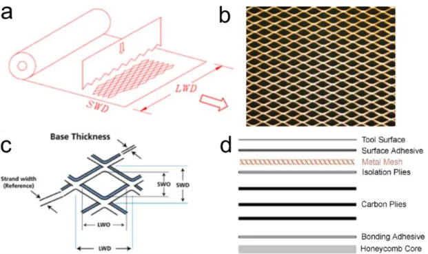
The aerospace industry’s common practice for protection of composite structures is the addition of a metallic mesh at the surface of the panel. The metals of choice are aluminum or copper, with respective conductivities of 3.77×10⁷ and 5.96×10⁷ S/m. While lighter than copper, aluminum has a high galvanic potential difference with graphite and therefore needs to be further isolated from the structure by adding a protective layer which adds weight to the aircraft [22]. Copper eliminates the threat of galvanic corrosion at the expense of adding weight. Metal meshes can be either woven or expanded.
Figure 2.8 illustrates the fabrication processes and parameters of expanded metal meshes. These meshes start as a metal foil that is slit with a dye in an alternating pattern (Figure 2.8a) and expanded to form diamond-shaped openings [22-24]. The extent of the expansion controls the size of the long way of the diamond (LWD) and short way of the diamond (SWD) measurements which will influence the conductivity in the two principal directions of the mesh.
Woven meshes are woven from metal strands in a simple plain weave. Woven meshes are subject to loosening of the strands which introduces additional contact resistance at the wire junctions. Also, the extra thickness at the wire intersections alter the surface finish [23, 24]. For integration on the composite surface, metal meshes are often sold integrated in a B-staged surfacing film and used against the tool surface as a prepreg in the composite layout (Figure 2.8d).
Figure 2.8: Expanded metal meshes. a) Fabrication method where a die cuts openings in a metal foil. The foil is then expanded in the direction indicated by the arrow [8]. b) Picture of an expanded copper mesh [25]. c) Fabrication parameters, SWD: short way of the diamond. LWD:
long way of the diamond [25]. d) Typical stacking of layers on a composite panel [8] Figure 2.9 shows the characteristics of prepreg systems incorporating metal meshes from two different manufacturers [26, 27]. Parameters of interest are the respective mass of the conductive mesh and of the resin, which lead to the calculation of the specific conductivity, defined as the sheet conductivity per unit mass. Typical sheet conductivities are of the order of 1×10⁻³ ohms per square (Ω/□), as calculated by taking the resistivity of an uniform metallic foil of areal weight equivalent to that of the mesh. The aluminum solutions provide a distinct advantage because of the much lower density of the metal, even when taking into account an additional 80 gsm insulation layer to protect the carbon plies against galvanic corrosion [26]. The solutions provided by Henkel on the other hand have a comparatively low amount of resin which helps in keeping the weight penalty low. It can also be argued that eliminating the need for a protective layer simplifies the manufacturing process and thus helps reduce costs.
The macroscopic interweaving of metallic and polymeric materials in metal meshes prepregs induce a localized mismatch between coefficients of thermal expansion, which in turn causes microcracking which can lead to corrosion of the mesh and a loss of conductivity. This effect was
shown to be more important with Al than with Cu, and the effect of the insulation fiberglass layer was also shown to be detrimental [28].
Repairs to the metal meshes can be problematic. Each lightning strike requires that the aircraft’s skin be repaired. First, the damaged structural portion of the existing panel has to be removed and replaced according to state of art repair methods [29]. Damaged plies have to be fully cured before the actual LSP system repair, considered a separate operation [30], can start. The intact LSP system then must be exposed so that the patch can be carefully aligned and connected to the exposed strands. It is critical that the connectedness of the repaired metal mesh be verified with a milliohm meter [30]. When lightning strikes a poorly repaired panel, the damage observed is catastrophic, in some cases even worse than for unprotected panels [9].
Figure 2.9: Areal weight of different commercial expanded metal mesh LSP prepregs along with the corresponding calculated specific conductivity [26, 27]
2.3.2 Alternative commercial solutions.
Hexcel commercializes an E-glass structural fabric that has been aluminized to provide sufficient conductivity for Zone 1 applications, according to the manufacturer [31]. The company lists a nominal resistivity of “5-10 Ω/ft2” [sic.]. Considering the intention was to specify sheet resistance, the specific conductivity obtained is 6.94-3.47 S·cm2/gwith resin weight left out of the calculation. Lord Corp. developed a product, available as spray-on coating or as a film, based on the segregation of metallic particles during curing [32]. The metallic fillers with dimensions in the range of a few
tens of microns are coated with a non-polar material whereas the matrix comprises polar moieties. Upon curing a kinetically driven process occurs in which the filler particles migrate and aggregate to form a conductive network. Silver flakes are the preferred filler particles for their ability to sinter at low temperatures and their high conductivity [32]. Although not mentioned in the text, it is reasonable to suppose that the elongated shape of silver flakes also contributes in establishing the conductive network. Considering data given in [33] and a matrix density of 1.2 g/cm3, the calculated specific conductivity is ~9.1×10³ S·cm2/g.
Conductive Composites proposes CVD Ni coated carbon and aramid fibers as well as Ni nanostrands to enhance conductivity in composites, which they claim have been proven suitable for LSP [34]. Their proprietary process allows a continuous fabrication of the fabrics. The heaviest available fabric is also the most effective with a sheet resistivity of 0.015 Ω/□, for a specific conductivity of ~1×10⁴ S⸱cm2/g, albeit without factoring in the resin impregnation. An interesting fact about this technology is that it has potential to yield truly multifunctional systems as the conductive plies can be structural.
2.4 On the influence of layup on LSP performance
In aluminum fuselages, the bulk of the structural material participates in the conduction of lightning energy. Conversely, composite systems are made of different layers of material. This raises the question as to what stack up sequence should be promoted for LSP applications.
Recently, Han et al. [35] investigated the severity of the damage caused by emulated lightning strikes on composite coupons protected with carbon nanotube papers bonded to the underlying composite. Bonding was performed either with a conductive carbon nanotube loaded epoxy resin, a conventional insulating neat resin or a highly insulating boron nitride filled resin, respectively serving the roles of conductivity enhancer, conductivity benchmark and insulating barrier. The LSP system used is represented in Figure 2.10. The authors conclude that using an electrically insulating adhesive layer, although it does not allow conduction through the thickness and thus limits the volume were lightning energy is dissipated, yields better protection of the composite samples. The effect of the dielectric barrier was further studied in numerical simulations by Fu et al. [36] who replicated the layup from the Han et al. paper, shown in Figure 2.10. They incorporated the electrical breakdown behavior of the adhesive layer in the ABAQUS simulation through user
subroutines. Their results are in excellent agreement with the conclusions from the Chinese group of Han et al. as they show that LSP systems incorporating a high dielectric strength layer between the conductive film and the substrate could withstand higher currents than their counterparts with conductive interlayers.
Figure 2.10: Disposition of the different layers in the prospective LSP system investigated by Han et al. a) As-produced buckypaper. b) Layer structure of LSP system. Reproduced from [35]
2.5 Potential materials for lightning strike protection
Metal meshes used for LSP are based on a 100 year-old technology for mesh fabrication that was introduced as a quick solution to a problem that was not fully recognized on the dawn of the composite era in aerospace [22]. The industry is thus awaiting new solutions that would minimize
the weight penalty associated with LSP solutions. Here are presented different avenues that hold potential for LSP applications.
2.5.1 Carbon nanotubes
Carbon nanotubes have perhaps been the center of attention of the most important body of materials science research of the early 21st century for their outstanding electrical and mechanical properties. One could not study conductive composites without taking a glance at what promises this technology holds.
2.5.1.1 Physics and morphology
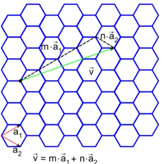
In their simplest form, carbon nanotubes are rolled-up single sheets of honeycomb-structured sp2 hybridized carbon atoms capped with fullerenes of typical diameter of 1-2 nm [37]. Figure 2.11 illustrates the honeycomb structure on a planar geometry. Nanotubes can exist in a multi-sheet configuration and are then called Multi-Walled Carbon Nanotubes (MWCNTs) as opposed to Single-Walled Carbon Nanotubes (SWCNTs). SWCNTs can have their honeycomb lattice wrapped in three different families of configurations: zigzag, armchair and chiral. The classification relies on the chiral vector of the nanotube. Figure 2.11 illustrates the basis lattice vectors and the construction of a chiral vector. The basis vectors of the graphene structure (honeycomb planar structure of C atoms) are a set of vectors (𝑎𝑎1, 𝑎𝑎2) defined so that every position in the lattice can be reached with a translation by a vector 𝑣𝑣⃗ = 𝑚𝑚 ⋅ 𝑎𝑎����⃗ + 𝑛𝑛 ⋅ 𝑎𝑎1 ����⃗. The chiral vector is 2 defined as the translation around the circumference of the tube that brings back to the same lattice point by cylindrical symmetry.
Figure 2.11: Basis vectors of graphene crystal structure. The chiral vector of a SWCNT is expressed as a linear combination of the basis vectors a1 and a2
Therefore, each chiral vector can be described by a pair of integers (𝑛𝑛, 𝑚𝑚). Special cases of chirality are the zigzag and armchair configuration. For a zigzag nanotube 𝑛𝑛 = 0 ⋁ 𝑚𝑚 = 0. For the armchair configuration 𝑛𝑛 = 𝑚𝑚. All other combinations are termed “chiral”.
Chirality affects the electronic band structures in such a way that some configurations exhibit a band gap at the Fermi energy1 and thus behave like a semiconductor [37, 38]. The condition for metallicity is simply expressed as [37]:
𝑛𝑛 − 𝑚𝑚 = 3𝑖𝑖, (1)
where i is an integer. Consequently, approximately only 33% of SWNCT’s are metallic. The linear dispersion relation of energy levels at the Fermi energy in graphene structure leads to null effective mass of electrons. The electrons are therefore relativistic particles and ballistic conduction can occur [39-41]. Theory then predicts exceptional electron mobility in carbon nanotubes. High SWCNT current densities up to 109 Acm-2 have been measured [42]. SWCNT have been
1 The energy between the highest occupied and the lowest unoccupied levels considering electrons in their ground
theoretically calculated to have a resistivity per unit length as low as 4.2 kΩ/µm [43], which yields a conductivity of 1.35×10⁶ S/cm, using an average tube diameter of 1.5 nm. The corresponding specific conductivity is therefore at least 5.9×10⁵ S⸱cm2/g, using the density of graphite.
MWCNTs usually exhibit a metallic behavior in their electrical properties as well as an increase in conductivity with temperature [44]. It was shown that multiple walls participate in current transfer [45] and that multiple channel ballistic conduction was feasible [46]. Stetter measured the resistance of individual multi-wall carbon nanotubes by scanning the potential values along the length of the tubes. This method allowed decoupling of the contribution of different shells to the overall resistivity. Values of the order of 10 kΩ/µm were consistently obtained [47]. Ebbesen et al. [48] measured the electrical conductivity on pristine isolated MWCNTs of different diameters. Their results2 ranged between 2.5×10² and 2×10⁵ S/cm with an observed current density of 6×10⁶ A⸱cm2. Care must however be taken with the interpretation of these results since prior to the measurements, the nanotubes were irradiated with 30 keV Ga ions which are known to damage and cut nanotubes [49].
2.5.1.2 Dispersion in solution
To control the distribution of nanotubes in a material, the dispersion of the particles must be achieved prior to the reorganization in the desired configuration. Dispersion of nanotubes into solution represents a challenge, with the only known efficient CNT dispersant being chlorosulfonic acid [50, 51], a hazardous superacid which protonates the surface of CNTs to induce electrostatic repulsion. The weak π−π interaction between adjacent carbon nanotubes coupled with the high aspect ratio of the particles increase the tendency of CNTs to bundle [52]. Chemical dispersion methods include covalent and non-covalent functionalization [53]. Covalent functionalization is obtained by attaching moieties to the tips or sidewalls of nanotubes. The covalent nature of the modification means implies that the functionalization is associated with a change of hybridization from sp2 to sp3 and therefore introduces defects in the electronic structure of the CNT [54].
Non-covalent functionalization can be achieved with polymers or surfactants. Polymers wrap around the nanotubes to form a molecular complex. The functional groups of the polymer then
become available for the dispersion of CNTs [54]. Surfactants adsorb on the CNT surface in a non-covalent way. The surfactants can encapsulate CNTs in a micelle entirely, create semi-spherical micelles on the surface or adsorb at random sites on the surface [52]. Non-covalent functionalization has the advantage of being non-destructive to the crystal structure. Chemical functionalization must be complemented with mechanical dispersion methods o provide the energy necessary for the initial separation of the tubes [52]. Among these, ultrasonication is the most widely used. It is accomplished by generating ultrasonic waves in the dispersion media through a vibrating tip or through the walls of a vessel. The short-wavelength shockwaves cause nanotubes on the bundle’s periphery to dislodge and isolate [54]. Functional groups then prevent the nanotubes from rebundling by providing an electrochemical and physical barrier to the van der Walls close range interactions.
2.5.1.3 Buckypapers
A film of CNTs is called a buckypaper. These structures are often fabricated using vacuum filtration [55-62], a method in which nanotubes are dispersed into solution before being filtered through a microporous membrane. As the solvent is removed, individual CNTs settle in the plane of the filter media in a morphology analogous to that of random chopped fiber mats [59]. After drying, the film can be peeled off the filter. Table 2.2 lists different values for the electrical performance of buckypapers found in literature. The bulk conductivity of carbon nanotubes in buckypapers differs significantly from that of individual nanotubes with reported values ranging from 100 to 6200 S/cm [61, 63].
In their pristine state, buckypapers have poor electrical properties when compared to single CNTs. However, chemical treatments such as oxidation and doping [64] and chemical crosslinking [63] can improve their electrical performance. Remarkably, Chen et al reported a 10-fold improvement of buckypaper electrical properties upon HNO3 treatment and cross-linking with 10,12-pentacosadiyn-1-OL (PCDO). Resistivity was further enhanced by aligning the nanotubes through stretching [63].
Park et al. [65] investigated the electromagnetic interference shielding properties of buckypaper laminated composites. Table 2.2 lists the resistivity of the different buckypapers investigated. The results from [63, 65] suggest that long MWCNTs exhibit better bulk conductivity than SWCNTs.
Furthermore, an anti-synergistic effect appears to arise from the mixing of SWCNTs and MWCNTs.
Tenent et al. [66] fabricated large area films of SWCNTs by a spray deposition technique. SWCNTs were dispersed in a carboxymethyl cellulose (CMC) solution which was then fed to an ultrasonic spraying nozzle. The dispersion was sprayed on a substrate and allowed to dry before soaking in 4M HNO3 for removal of CMC. The films produced exhibited a specific conductivity of ~1.2×10⁴ S·cm2/g, comparable to that of leading LSP solutions (see Table A.1 in Appendix A). Han et al. whom we have discussed briefly in Section 2.4, tested a LSP system using a layup of CFRP/adhesive/buckypaper wherein the adhesive can be either neat epoxy, conductive CNT-filled epoxy or insulating boron nitride-filled epoxy. Their buckypaper is made by dispersion in water/triton X-100 and subsequent filtration through polyvinylidene fluoride membranes and intensive deionized water flushing to remove the adsorbed surfactant [67]. The surface conductivity of the protected composite coupons was reported to be of 0.83 S/□ for a volume conductivity of 57 S/cm, which lies in the low range of other buckypapers reported values (see Table 2.2). By using a ~200µm BN-filled insulating adhesive layer, the authors showed that simulated lightning strikes with peak currents up to 100 kA could be sustained by the test coupons. This is interesting since the specific conductivity obtained is of ~85 S⸱cm2/g, a rather modest value when compared to copper meshes that lie in the 104S⸱cm2/g range.
![Figure 2.2: Aircraft-initiated lightning strike on takeoff. Leaders expanding away from plane can be clearly seen [16]](https://thumb-eu.123doks.com/thumbv2/123doknet/2326814.30641/30.918.227.697.105.725/figure-aircraft-initiated-lightning-takeoff-leaders-expanding-clearly.webp)
![Figure 2.3: Illustration of the lightning channel reattachment process. Ec is the critical breakdown electric field and Vinf is the relative speed of the plane to the viscous media [18]](https://thumb-eu.123doks.com/thumbv2/123doknet/2326814.30641/31.918.118.786.305.516/illustration-lightning-reattachment-critical-breakdown-electric-relative-viscous.webp)
![Table 2.1: Peak currents and action integrals for cloud-to-ground flashes [19]](https://thumb-eu.123doks.com/thumbv2/123doknet/2326814.30641/32.918.161.758.346.473/table-peak-currents-action-integrals-cloud-ground-flashes.webp)
![Figure 2.6: Lightning strike zoning per ARP5414 [17]. Adapted from [21]](https://thumb-eu.123doks.com/thumbv2/123doknet/2326814.30641/35.918.121.810.216.571/figure-lightning-strike-zoning-per-arp-adapted-from.webp)
![Figure 2.7: Standardized current test waveform per [19]. Component A represents the first return stroke and applies only to Zone 1 areas](https://thumb-eu.123doks.com/thumbv2/123doknet/2326814.30641/36.918.204.720.110.443/figure-standardized-current-waveform-component-represents-return-applies.webp)
![Figure 2.9: Areal weight of different commercial expanded metal mesh LSP prepregs along with the corresponding calculated specific conductivity [26, 27]](https://thumb-eu.123doks.com/thumbv2/123doknet/2326814.30641/39.918.104.811.428.732/different-commercial-expanded-prepregs-corresponding-calculated-specific-conductivity.webp)