UNIVERSITÉ DE MONTRÉAL
CHARACTERIZATION OF INTERCONNECTION DELAYS IN FPGAS DUE TO SINGLE EVENT UPSETS AND MITIGATION
MOSTAFA DARVISHI
DÉPARTEMENT DE GÉNIE ÉLECRIQUE ÉCOLE POLYTECHNIQUE DE MONTRÉAL
THÈSE PRÉSENTÉE EN VUE DE L’OBTENTION DU DIPLÔME DE PHILOSOPHIAE DOCTOR
(GÉNIE ÉLECTRIQUE) AVRIL 2018
UNIVERSITÉ DE MONTRÉAL
ÉCOLE POLYTECHNIQUE DE MONTRÉAL
Cette thèse intitulée :
CHARACTERIZATION OF INTERCONNECTION DELAYS IN FPGAS DUE TO SINGLE EVENT UPSETS AND MITIGATION
présentée par : DARVISHI Mostafa
en vue de l’obtention du diplôme de : Philosophiae Doctor a été dûment acceptée par le jury d’examen constitué de :
M. SAWAN Mohamad, Ph. D., président
M. AUDET Yves, Ph. D., membre et directeur de recherche
M. BLAQUIÈRE Yves, Ph. D., membre et codirecteur de recherche M. SAVARIA Yvon, Ph. D., membre
DEDICATION
To my love, Masoumeh To the loving memory of my parents To my siblings, Fatemeh & Mahdi
ACKNOWLEDGEMENTS
First and foremost, it is a genuine pleasure, indeed honor, to express my sincere gratitude to my advisors, Professor Yves Audet and Professor Yves Blaquière for their understanding, insightful comments, meticulous scrutiny, enthusiasm and dynamism added considerably to my research experience and made an important part of this dissertation. It has been an honour and pleasure to purse the Ph.D. studies with both of you. This Ph.D. project could not be accomplished without your continuous support and inspiring guidance. I owe you my eternal gratitude for all I have learned from both of you, Thank you!
My sincere thanks go to the members of the examination jury, Professor Mohamad Sawan, Professor Yvon Savaria, and Professor Otmane Ait Mohamed for reading my thesis and providing their invaluable comments. I also would like to express my gratitude to Professor Claude Thibeault at ÉTS for his insightful comments and providing the financial support.
I would like to thank the faculty and staff members of Electrical Engineering Department at Polytechnique Montréal, especially Réjean Lepage and also Jean Bouchard for their technical assistance. My special gratitude extends to Mrs. Nathalie Lévesque for her assistance with all the administrative works. As I always have mentioned : “Nathalie, vous êtes vraiment comme
une maman gentille pour les étudiants de notre département…! Merci à vous”
At this point, I cannot forget the endless love and care of my late beloved parents who introduced me the joy of reading since the birth. You sacrificed your life to raise me with a true love to reach to this level with your compassion, kindness and unfailing support. Absolutely, you are always alive in my heart and I sense your presence whenever I feel loneliness. There is no day that I never remember you, talk to you and ask you to pray for me! May your gentle souls rest in peace my beloved Mom and Dad! Thank you! I also would like to express my deepest thanks to my beloved siblings, Fatemeh and Mahdi, for their endless love, encouragement, and prayers.
The last, but absolutely not the least, I would like to thank my love, Masoumeh for her extraordinary and unconditional love and kindness who has touched my heart with her lovely eyes! I am very much indebted to her for accompanying me faithfully. She also sacrificed a lot of time to help me transform my scribbling into a readable thesis. Thank you my dear!
RÉSUMÉ
L’utilisation incessante de composants électroniques à géométrie toujours plus faible a engendré de nouveaux défis au fil des ans. Par exemple, des semi-conducteurs à mémoire et à microprocesseur plus avancés sont utilisés dans les systèmes avioniques qui présentent une susceptibilité importante aux phénomènes de rayonnement cosmique. L'une des principales implications des rayons cosmiques, observée principalement dans les satellites en orbite, est l'effet d'événements singuliers (SEE). Le rayonnement atmosphérique suscite plusieurs préoccupations concernant la sécurité et la fiabilité de l'équipement avionique, en particulier pour les systèmes qui impliquent des réseaux de portes programmables (FPGA). Les FPGA à base de cellules de mémoire statique (SRAM) présentent une solution attrayante pour mettre en œuvre des systèmes complexes dans le domaine de l’avionique. Les expériences de rayonnement réalisées sur les FPGA ont dévoilé la vulnérabilité de ces dispositifs contre un type particulier de SEE, à savoir, les événements singuliers de changement d’état (SEU). Un SEU est considérée comme le changement de l'état d'un élément bistable (c'est-à-dire, un bit-flip) dû à l'effet d'un ion, d'un proton ou d’un neutron énergétique. Cet effet est non destructif et peut être corrigé en réécrivant la partie de la SRAM affectée.
Les changements de délai (DC) potentiels dus aux SEU affectant la mémoire de configuration de routage ont été récemment confirmés. Un des objectifs de cette thèse consiste à caractériser plus précisément les DC dans les FPGA causés par les SEU. Les DC observés expérimentalement sont présentés et la modélisation au niveau circuit de ces DC est proposée. Les circuits impliqués dans la propagation du délai sont validés en effectuant une modélisation précise des blocs internes à l'intérieur du FPGA et en exécutant des simulations. Les résultats montrent l’origine des DC qui sont en accord avec les mesures expérimentales de délais. Les modèles proposés au niveau circuit sont, aux meilleures de notre connaissance, le premier travail qui confirme et explique les délais combinatoires dans les FPGA.
La conception d'un circuit moniteur de délai pour la détection des DC a été faite dans la deuxième partie de cette thèse. Ce moniteur permet de détecter un changement de délai sur les sections critiques du circuit et de prévenir les pannes de synchronisation engendrées par les SEU sans utiliser la redondance modulaire triple (TMR). Cette méthode conserve la fonctionnalité du
système en abaissant temporairement la fréquence d’opération pour éviter une panne de délai jusqu’à ce que le bit défectueux responsable ait été corrigé.
La sensibilité aux SEU du réseau d'interconnexions programmable dans un FPGA de la famille Zynq-7000 est validée expérimentalement sous bombardement de neutrons. Une méthode pour configurer une architecture d’oscillateurs en anneau, principalement avec des ressources de routage et un minimum de ressource logique, est proposée. Un contrôle total des ressources de routage permet de cibler les différents types d’interconnexions disponibles dans le FPGA et de créer des oscillateurs dont la fréquence est fixée par la longueur du routage (RO). De plus, un algorithme de routage à travers des matrices de commutation est présenté pour identifier automatiquement les points d'interconnexion programmables associés à une paire d’interconnections. Une configuration expérimentale pour mesurer sans équipement externe les DC sur les différents types de routage dans le FPGA est proposée. Les résultats expérimentaux montrent que la configuration permet de mesurer des DC induits par SEU aussi faible que 8 psec. Il est également démontré que les différents types d’interconnexion présentent différentes durées moyennes avant l’apparition d’un DC.
ABSTRACT
The unrelenting demand for electronic components with ever diminishing feature size have emerged new challenges over the years. Among them, more advanced memory and microprocessor semiconductors are being used in avionic systems that exhibit a substantial susceptibility to cosmic radiation phenomena. One of the main implications of cosmic rays, which was primarily observed in orbiting satellites, is single-event effect (SEE). Atmospheric radiation causes several concerns regarding the safety and reliability of avionics equipment, particularly for systems that involve field programmable gate arrays (FPGA). SRAM-based FPGAs, as an attractive solution to implement systems in aeronautic sector, are very susceptible to SEEs in particular Single Event Upset (SEU). An SEU is considered as the change of the state of a bistable element (i.e., bit-flip) due to the effect of an energetic ion or proton. This effect is non-destructive and may be fixed by rewriting the affected part.
Sensitivity evaluation of SRAM-based FPGAs to a physical impact such as potential delay changes (DC) has not been addressed thus far in the literature. DCs induced by SEU can affect the functionality of the logic circuits by disturbing the race condition on critical paths. The objective of this thesis is toward the characterization of DCs in SRAM-based FPGAs due to transient ionizing radiation. The DCs observed experimentally are presented and the circuit-level modeling of those DCs is proposed. Circuits involved in delay propagation are reverse-engineered by performing precise modeling of internal blocks inside the FPGA and executing simulations. The results show the root cause of DCs that are in good agreement with experimental delay measurements. The proposed circuit level models are, to the best of our knowledge, the first work on modeling of combinational delays in FPGAs.
In addition, the design of a delay monitor circuit for DC detection is investigated in the second part of this thesis. This monitor allowed to show experimentally cumulative DCs on interconnects in FPGA. To this end, by avoiding the use of triple modular redundancy (TMR), a mitigation technique for DCs is proposed and the system downtime is minimized. A method is also proposed to decrease the clock frequency after DC detection without interrupting the process. The susceptibility of the programmable interconnection network in a state-of-the-art Zynq-7000 FPGA family to SEU is experimentally validated. It is known that a bit-flip induced by an SEU in the routing network leads to an undesired bridge between an unrouted interconnect and a live
interconnect. A method to configure architectures mostly with routing resources and minimal logic resources is proposed. A full control over routing resources enables us to employ different interconnections available in the FPGA in order to create routing-based ring oscillators (RO). In addition, a novel algorithm enabling the configuration of routing paths through switch matrices, which automatically identify interconnection points between a pair of interconnections is presented. An experimental setup to measure DCs on the routing resources of an APSoC is proposed. The experimental results show that the proposed setup, requiring no external equipment for DC measurement, is able to measure induced DCs as low as 8 psec. It is also shown that different interconnection types presents different mean time before DC occurrence.
TABLE OF CONTENTS
1.1 Motivation ... 1
1.2 Background on Radiation Effects ... 2
1.2.1 Radiation Effects on Electronic Devices ... 2
1.2.2 Single-Event Effect (SEE) ... 3
1.2.3 SEE Classification ... 5
1.2.4 Single-Event Upset (SEU) ... 7
1.2.5 Other Destructive Phenomena ... 8
1.3 Xilinx Virtex-5 SRAM-Based FPGA ... 10
1.3.1 Virtex-5 CLB Overview ... 10
1.3.2 Virtex-5 Slice Configuration ... 12
1.3.3 Virtex-5 Interconnection Network... 13
1.3.4 SEU Controller Macro ... 14
ACKNOWLEDGEMENTS ... IV RÉSUMÉ ... V ABSTRACT ...VII TABLE OF CONTENTS ... IX LIST OF TABLES ... XIV LIST OF FIGURES ... XV LIST OF SYMBOLS AND ABBREVIATIONS... XIX LIST OF APPENDICES ... XXIV CHAPTER 1 INTRODUCTION ... 1
1.4 Fault Models in the SRAM-based FPGA Resources ... 14
1.4.1 Fault Model in PIPs ... 14
1.4.2 Fault Model in Buffers ... 15
1.4.3 Fault Model in Multiplexers ... 17
1.4.4 Fault Model in LUTs ... 17
1.4.5 Fault Model in Switch Matrices ... 18
1.4.6 Fault Model in Slice Registers ... 18
1.4.7 Fault Model in IOBs ... 20
1.5 AVIO-403 Project ... 21
1.6 EPICEA Project ... 21
1.7 Problem Definition ... 22
1.8 Objectives ... 24
1.9 Research Contributions ... 25
1.10 Organization of the Thesis ... 26
1.11 Summary ... 26
2.1 Introduction ... 28
2.2 SEU Effects in Digital ICs ... 28
2.3 Radiation Experiments on FPGAs ... 30
2.4 SEU Mitigation Techniques in FPGAs ... 34
2.4.1 Triple Modular Redundancy (TMR) ... 35
2.4.2 Partial Reconfiguration ... 36
2.5 SEU Detection Techniques in FPGAs ... 39
2.5.1 Readback and Comparison ... 39
2.5.2 Cyclic Redundancy Check (CRC) ... 40
2.5.3 Off-line test ... 40
2.5.4 Roving test ... 40
2.6 SEU Correction Techniques in FPGAs ... 41
2.6.1 SEU Detection and Single Frame Correction ... 41
2.6.2 SEU Scrubbing (Active Partial Reconfiguration) ... 42
2.7 Review of TDCs Implemented in FPGAs ... 42
2.8 Delay Fault Detection and Test ... 45
2.9 Routing Fault Detection and Correction ... 56
2.10 Coherence of the Articles in Relation to the Research Goals ... 57
2.11 Summary ... 58
3.1 Overview ... 60
3.2 Abstract ... 60
3.3 Introduction ... 61
3.4 Background on Extra Combinational Delays in SRAM-Based FPGAs ... 62
3.5 FPGA Circuit-Level Models for ODC Root Cause Validation ... 63
3.5.1 Circuit Level Models ... 63
3.5.2 Model Configuration Tuning ... 65
3.6 Circuit Level Configurations Inducing ODCs in FPGA Core ... 68
3.6.1 Models for Delay Change Due to Extra Parasitic Interconnects ... 68
3.6.2 Models for Delay Change Due to SEU Effect on IMUX ... 71
3.6.3 Models for Delay Change Due to Extra Stuck-at Parasitic Interconnect ... 72
CHAPTER 3 ARTICLE 1 : CIRCUIT LEVEL MODELING OF EXTRA COMBINATIONAL DELAYS IN SRAM-BASED FPGAS DUE TO TRANSIENT IONIZING RADIATION ... 60
3.7 Comparison of Simulated and Measured Delays ... 74
3.7.1 Delay Fault Results in Virtex-5 FPGA Core ... 74
3.7.2 Delay Fault Results in Virtex-5 FPGA IOB ... 77
3.8 Conclusion ... 80
4.1 Overview ... 81
4.2 Abstract ... 81
4.3 Introduction ... 82
4.4 Real-Time Monitor for Delay Change Detection ... 84
4.5 Cumulative Delay Change Detection ... 88
4.5.1 Sensitivity to Cumulative Delay Changes ... 88
4.5.2 Proposed Algorithm for Detection of Cumulative Delay Changes ... 89
4.6 Experiments and Results ... 92
4.6.1 Test Bench ... 92
4.6.2 Experimental Validation of the Proposed DC Monitor ... 93
4.6.3 Experiments to Detect Cumulative Delay Change (CDC) ... 96
4.7 Conclusion ... 99
4.8 Acknowledgment ... 99
5.1 Overview ... 100
5.2 Abstract ... 100
5.3 Introduction ... 101
CHAPTER 4 ARTICLE 2 : DELAY MONITOR CIRCUIT AND DELAY CHANGE MEASUREMENT DUE TO SEU IN SRAM-BASED FPGA ... 81
CHAPTER 5 ARTICLE 3 : ON THE SUSCEPTIBILITY OF SRAM-BASED FPGA ROUTING NETWORK TO DELAY CHANGES INDUCED BY IONIZING RADIATION ... 100
5.4 Background ... 103
5.5 Overview of Routing Resources in Zynq-7000 APSoC ... 104
5.5.1 Logic and Interconnect Tiles Resources ... 104
5.5.2 Interconnect Types Available in 7-Series FPGAs ... 105
5.5.3 PIP Notion and Interconnect Coordinate ... 107
5.6 Identification of Extra Interconnects Linked to a Logical Net ... 109
5.6.1 Routing Algorithm for Switch Matrices ... 109
5.7 Proposed Architecture for Delay Change Evaluation ... 112
5.8 Experiments and Results ... 115
5.8.1 Setup ... 115
5.8.2 Results and Discussion ... 117
5.9 Conclusion and Future Works ... 126
5.10 Acknowledgment ... 126
7.1 Concluding Remarks ... 130
7.2 Scope for Future Work ... 132
CHAPTER 6 GENERAL DISCUSSION ... 127
CHAPTER 7 CONCLUSION AND FUTURE WORKS ... 130
BIBLIOGRAPHY ... 133
LIST OF TABLES
Table 2-1 : Comparison matrix of fault detection methods ... 41
Table 3-1 : Simulated configurations for ODC root cause validation reported in Figure 3-12 ... 76
Table 4-1 : Comparison of our proposed monitor with alternative methods ... 95
Table 4-2 : Occurrence of DC increase with DC level ... 98
Table 5-1 : Types and number of interconnects linked to each WSM in 7-series FPGAs [182] ... 107
Table 5-2 : Characteristics of the implemented ROs to the FPGA ... 113
Table 5-3 : Estimated induced DC value corresponding to each interconnect type ... 121
LIST OF FIGURES
Figure 1-1 : Charge generation (A), collection and transport (B), (C) phases in a reverse-biased
junction and the resultant current pulse caused by the passage of a particle (D) [7] ... 4
Figure 1-2 : SEE classification [11] ... 6
Figure 1-3 : SEU and MBU in the sequential logic and SET in the combinational logic [5] ... 9
Figure 1-4 : Bulk CMOS inverter architecture cross-section showing the parasitic bipolar SCR structure susceptible to SEL [16], [17] ... 9
Figure 1-5 : Matrix architecture of Xilinx Virtex-5 FPGA [25], [26] ... 11
Figure 1-6 : Slice architecture in Xilinx Virtex-5 FPGA [24] ... 12
Figure 1-7 : Partial interconnection network in Xilinx Virtex-5 FPGA [28] ... 13
Figure 1-8 : PIP failure models due to an injected SEU [32] ... 15
Figure 1-9 : Fault models for buffers due to an injected SEU [33] ... 16
Figure 1-10 : Fault model for multiplexer due to an injected SEU [33] ... 17
Figure 1-11 : Fault model for LUT [33] ... 19
Figure 1-12 : SM model and SEU effect [28] ... 19
Figure 1-13 : Fault model in slice register due to SEU effect ... 20
Figure 1-14 : IOB model for Xilinx Virtex FPGA [28] ... 20
Figure 2-1 : Simulation of SRAM cell to investigate SEE [38] ... 29
Figure 2-2 : SEU sensitive areas in a CLB in FPGA [62]... 32
Figure 2-3 : Simplified view of the bit flip impact on an implemented 2-input AND gate : (A) Fault free implementation, (B) an open case, (C) a short case, and (D) a delay case [32] .... 33
Figure 2-4 : Experimental results indicating ODCs observed in [32] ... 34
Figure 2-5 : Basic premise of partial reconfiguration [74]... 38
Figure 2-6 : Partial dynamic reconfiguration process [62] ... 39
Figure 2-8 : Simplified circuit diagram of a tapped delay line [92] ... 44
Figure 2-9 : Delay fault BIST architecture studied in [89] ... 46
Figure 2-10 : Presented ATPG architecture for delay fault detection in [107] ... 47
Figure 2-11 : Segment delay fault model presented in [107] ... 48
Figure 2-12 : TIMBER-based error detection and error masking technique [109] ... 50
Figure 2-13 : Dedicated TIMBER flip-flop (A), and clock control design (B) [109] ... 51
Figure 2-14 : Digital circuit implementation of time-domain majority voter; with delayed clock signals (A), and with delayed output signal (B) [110] ... 52
Figure 2-15 : Time dilation flip-flop for error detection and correction studied in [113] ... 53
Figure 2-16 : Sensor architecture presented in [114] ... 55
Figure 3-1 : Experimental setup used by AVIO403 team at TRIUMF to measure extra delays [32] ... 63
Figure 3-2 : Model of a two configurations of slice to slice interconnection in Virtex-5 ... 64
Figure 3-3 : Switch matrix structure reported by Xilinx FPGA Editor including our equivalent circuit for the second configuration ... 65
Figure 3-4 : Structure of slice-to-slice interconnection A) between two adjacent CLBs, B) in a single CLB ... 66
Figure 3-5 : Delay variation as a function of short interconnection length for the configurations used to define LCC in Figure 3-4A and LSS in Figure 3-4B ... 67
Figure 3-6 : Effect of an SEU on a Programmable Interconnection Point (PIP) in SB, adding a combinational delay : A) 1 ODC case (1 SEU), B) 2 ODC case (2 SEUs) ... 69
Figure 3-7 : A sequence of three SEUs connecting three interconnects of length 1LCC to the main routing path ... 70
Figure 3-8 : Examples of various interconnection lengths in Virtex-5 FPGA [129, 137] ... 71
Figure 3-9 : Mechanism of delay change creation in IMUX circuit ... 72
Figure 3-11 : Delay change mechanism in ring oscillator by additional cross lines stuck at ‘0’ or
‘1’ induced by SEU ... 74
Figure 3-12 : Histogram of measured delays at TRIUMF [32] and simulated delays for the ring oscillators implemented in the core of FPGA ... 75
Figure 3-13 : Implementation of two ring oscillators created by Virtex-5 IOBs [140] ... 78
Figure 3-14 : Histogram of measured delays at TRIUMF [36], emulation and simulated delays for the ring oscillators implemented inside the FPGA utilizing the Virtex-5 IOBs ... 79
Figure 4-1 : Timing issues in synchronous circuits : SEU implication on a configuration bit of interconnections or switch boxes associated with logic cone of SUT ... 84
Figure 4-2 : DC Monitor architecture for delay change detection (A). Its timing diagram is shown without delay change (B), and with delay change (C) ... 85
Figure 4-3 : Levels of SEU connecting parasitic interconnects to the SUT's logic cone resulting in CDC occurrence ... 89
Figure 4-4 : Flow graph of level 2 DC detection ... 90
Figure 4-5 : Proposed recursive pseudo-code (DFS) for DC detection ... 92
Figure 4-6 : The test bench configured to validate the delay monitor’s functionality ... 93
Figure 4-7 : Post place and route simulation results of SDC detection scheme using the DC monitor ... 94
Figure 4-8 : Experimental result of SDC detection obtained by ChipScope Pro Analyzer (ILA) . 94 Figure 4-9 : DC bins and maximum bin values for detected level 1, level 2, and level 3 DCs extracted from STA ... 96
Figure 4-10 : Three sets of experimental results for CDC detection ... 97
Figure 4-11 : Distribution of all detected DCs by twelve employed monitors with threshold DC values shown as the bins ... 98
Figure 5-1 : Topology of CLB and INT tiles in Xilinx 7-Series FPGAs extracted by Xilinx Vivado (Each CLB comprises two slices). Logical net NetA connects a source flip-flop to a destination LUT made of seven nodes each made of SINGLE (1L) interconnects ... 105
Figure 5-2 : Different topologies of DOUBLE (top) and SINGLE (bottom) interconnects in 7-Series FPGAs ... 108 Figure 5-3 : Interconnection of unrouted interconnects to NetA in different WSM levels due to
SEU implication for the example in Figure 5-1 ... 109 Figure 5-4 : Proposed algorithm for WSMs ... 111 Figure 5-5 : Extracted PIPs connected to LOGIC_OUTS2 and NN1BEG3 interconnects in
WSM1 and WSM4 ... 111 Figure 5-6 : Example of a directed routing in Vivado using TCL scripting ... 111 Figure 5-7 : Routing diagram for three different sets of ROs implemented to the FPGA : (a)
diagram of 1L, 2L, 4L and LONG interconnects, (b) diagram of BENTQUAD interconnects, and (c) diagram of BOUNCEACROSS and VQUAD interconnects ... 114 Figure 5-8 : (a) Diagram of experimental setup including DUT and reference (REF) ZedBoards;
(b) Interfacing two ZedBoards via FMC cable; (c) Front and top view of neutron beam shaft at TRIUMF lab ... 116 Figure 5-9 : One set of results obtained for the RO 4L configured with HQUAD interconnects.
The RO frequency decreases over time due to induced DCs ... 118 Figure 5-10 : One set of results obtained for the RO 4L configured with HQUAD interconnects
with GMM model and separated distributions ... 118 Figure 5-11 : Measured delay change values for all runs of RO BTQ ... 120 Figure 5-12 : All DC occurrences for each RO type observed in the course of 16 runs along with
simulation results ... 123 Figure 5-13 : DC time of occurrences for RO BTQ in the course of 16 run times ... 123
LIST OF SYMBOLS AND ABBREVIATIONS
ADL Adjustable delay line
APSoC All programmable system-on-chip ATGP Automatic test pattern generator BIST Built-in self test
BJT Bipolar junction transistor BRAM Block RAM
CDC Cumulative delay change
CDC Cumulative delay change
CEA Composite electric aircraft
CEU Code emulating upset
CEU code emulating upset
CLB Configurable logic block CLE Configurable logic element
CMT Clock management tile
CRC Cyclic redundancy check
CSA Canadian space agency
DC Delay change
DCM Digital clock manager
DFS Depth-first search
DLL Delay-locked loop
DMR Dual modular redundancy
DRAM Dynamic random access memory
DSET Digital SET
DSP Digital signal processor DUT Device/Design under test ECD Extra combinational delay ECD Extra combinational delay EDC Error detection and correction FPGA Field programmable gate array
FSM Finite state machine
GMM Gaussian mixture model
HDL Hardware description language
IBIS Input/output buffer information specification
IC Integrated circuit
ICAP Internal configuration access port
IEC International electrotechnical commission
ILA Integrated logic analyzer
IMUX Input multiplexer
IOB Input/output block
IP Intellectual property
ISS Instruction set simulator
ISS Instruction set simulator
LANSCE Los Alamos neutron science center LET Linear energy transfer
LPC low-pin-count
LUT Look-up-table
MBE Multiple-bit error
MBU Multiple bit upset
MTTDC Mean time to delay change
MTTF Mean time to failure
NoC Network-on-chip
ODC Observed delay change
PCORE Processor core
PDF Probability density function
PIP Programmable Interconnection Point
PL Programmable logic
PLL Phase-locked loop
PS Processor system
PUF Physical unclonable function PVT process-voltage-temperature
RO Ring oscillator
SB Switch box
SBE Single-bit error
SBU Single-bit upset
SCR Silicon-controlled rectifier
SDC Single delay change
SEB Single-event burnout
SEDR Single-event dielectric rupture
SEE Single-event effect
SEFI Single-event functional interrupt SEGR Single-event gate rupture
SEL Single-event latchup
SEM Single-event mitigation SESB Single-event snapback
SET Single-event transient
SEU Single-event upset
SEUC SEU controller
SHE Single hard error
SM Switch matrix
SoC System-on-chip
SOI Silicon-on-insulator
SRAM Static random access memory
STA Static timing analyzer STAR Self-testing area
SUT Signal under test
TDC Time-to-digital converter
TDL Tapped delay line
TMR Triple modular redundancy
TPG Test pattern generator
TRNG True random number generator
TSMC Taiwan semiconductor manufacturing company
VDL Vernier delay line
WSM Wilton switch matrix
LIST OF APPENDICES
CHAPTER 1 INTRODUCTION
1.1 Motivation
In the design of electronic systems, cosmic rays with high ionizing radiation levels are problematic challenges. A single charged particle can ionize thousands of electrons and create electronic noise and signal spikes [1]. In the case of digital circuits, this may cause failures or functional errors. CMOS electronic components are especially susceptible to ionizing radiations. This is a critical issue in the design of artificial satellites, airplanes, and mission aircrafts, since they contain a huge amount of electronic modules and components. In order to ensure the proper operation of such systems, integrated circuits (IC) manufacturers make efforts to design ICs and embedded systems which are more robust against cosmic rays.
Another limitation in today’s manufacturing industry (especially the spacecraft and aircraft providers using FPGAs) that makes the electronic devices very susceptible to ionizing radiation is technology down scaling. More specifically, as the feature sizes of components reduce, their sensitivity to ionizing radiations increase.
In avionic applications, as the aircraft traffic increases, new flight corridors should be defined at higher altitude that exposes the aircraft to more radiation. At the earth level, most of this radiation is absorbed by the atmosphere. However, on- board control devices are more exposed to radiation and hence the risk of an electronic fault is higher which could be a threat for passengers’ safety. The radiation usually generates single-event upset (SEU) by changing the state of a logical bit inside an integrated circuit and creating a soft error. Fortunately, SEUs are hardly destructive and may be fixed or avoided by proper circuit architectures or restoring algorithms.
In this thesis, SEUs occurring in SRAM-based FPGAs are studied due to their wide application range in aircraft electronic systems. The proper operation of an aircraft and its electronic components functionality must be guaranteed in high altitudes against cosmic rays. Therefore, it is of primary importance to develop mitigation techniques to ensure the robustness of FPGAs against ionizing radiations in order to reduce the on-board electronics downtime. In view of this, in collaboration with three industrial partners, i.e., Bombardier Aerospace, MDA Corporation, and Canadian Space Agency (CSA), the concerns on single-event effects (SEE) implications in FPGA-based applications intended for aircrafts travelling at high altitudes, are investigated.
1.2 Background on Radiation Effects
The presence of radiation is one of the effective elements to distinguish the space environment. The natural environment contains lots of electrons and protons that are trapped by planetary magnetic fields. Protons and a very small fraction of heavier nuclei are produced in energetic solar events and cosmic rays within and outside of our galaxy [2]. The cosmic rays consist of approximately 85% protons, 14% alpha particles, and 1% heavy ions, as well as x-ray and gamma-ray radiations. Although, most of these particles are filtered out by atmosphere, they still remain as a primarily concern for spacecrafts and the aircrafts travelling at high altitudes. This makes new challenges in avionic applications and space missions. When a particle beam interacts with materials, the secondary neutrons are created [3]. These neutrons can make a threat to SEEs in electronics. In addition, the protons are significant sources of creating SEEs especially in digital devices and embedded systems. For the charged particles, the amount of energy going into ionization is expressed by the stopping power or linear energy transfer (LET) function, commonly in units of or as energy per unit length in kiloelectronvolts per micrometer [2].
SEE phenomenon has primarily been observed only in orbiting satellites. However, since the beginning of 1980’s, by considering new flight corridors at higher altitudes, the SEE was defined as the main radiation concern for the avionics. SEE causes major concerns regarding the reliability and safety of avionic equipments, particularly for those systems that employ SRAM-based FPGAs for control and processing purposes. One particular type of SEE, namely SEU as a soft-error threats the reliability of SRAM-based FPGAs in avionics. As it will be considered throughout this thesis, the static memory cell of the SRAM-based FPGA is very susceptible to SEU. One of the main implications of this susceptibility that is considered in this work is the delay fault that has been thus far neglected in the literature. Following this section, some backgrounds on radiation effects, SEE and SEU implications in digital systems, as well as other phenomena caused by radiation will be drawn.
1.2.1 Radiation Effects on Electronic Devices
Statistical analysis and precise experimental designs in manufacturing companies have shown that the radiation effects are often the main cause of erroneous behavior of electronic
components, i.e., faults. These faults could be ignored in some applications. Though, for high reliability applications, especially in digital designs, it is essential to assess the faults caused by radiation effects. Among the problems in electronic systems caused by SEEs, a type of soft errors, also called SEU, is considered as the main challenge in avionic systems [4].
Although the ICs utilized in avionic systems operate in irradiative environments, they are sensitive to transient faults caused by interaction of ionizing particles with the silicon substrate of electronic components. In general, if a particle has the capability to divide a quite atom into ions, it is considered as an ionizing particle [5].
1.2.2 Single-Event Effect (SEE)
When a high-energy particle passes through a semiconductor, it creates an ionized track behind. This ionization may create a glitch in the output of the circuit or device, a bit-flip in the memory or a register, and a destructive latch-up and burnout in high-power transistors [6]. A bit-flip is defined as the change of the state of a bistable element, (e.g., a flip-flop or other memory elements) due to the effect of an energetic ion or proton. In designs without latches, it is recommended to employ RC time constant circuits in order to slow down the circuit response time during an SEE occurrence.
An SEE can be destructive or non-destructive. Destructive effects result in catastrophic device failure, while non-destructive effects will cause loss of data and/or control. The main implication of SEE is in the silicon substrate of semiconductor devices. When an ionizing particle strikes the silicon substrate, a nuclear reaction occurs between them caused by charge generation. The charge generated by single non-destructive strikes is collected and will produce a spurious voltage on a sensitive node of the design [2]. The charge can be deposited directly or indirectly into the material. For example, the neutron strikes will generate the secondary particles such as protons and alpha particles which are charged and may perturb the functionality of a electronic component of the circuit [5].
A single charged particle passes through an electronic component in three main successive steps, namely, the charge deposition by the energetic particle striking the sensitive region, transporting the released charge into the device, and the charge collection in the sensitive region of the device [7]. Figure 1-1 shows the three steps in the case of an energetic charged particle passing through
a reverse-biased junction [8]. The steps of this mechanism are described in more details in the following.
Charge deposition/generation : When the particle strikes the sensitive region of the inverse biased p-n junction, it collides with the crystal lattice of the semiconductor and penetrates to the substrate. Consequently, the ions are generated that transfer a large amount of energy to the electrons of the struck atoms and a cylindrical track of electron-hole pairs with a submicron radius is generated along the particle path (Figure 1-1A).
Charge Collection and transport : When the track of electron-hole pairs is generated in the semiconductor substrate, the released carriers are quickly transported and then collected by elementary structures (e.g., p-n junctions). The charge transport is performed through two mechanisms : charge drift in regions with an electric field (Figure 1-1B) and charge diffusion in neutral zones (Figure 1-1C) [7]. The transported charges in the device induce a parasitic transient current (Figure 1-1D), which may induce disturbances in the device and associated circuits. If the parasitic current is large enough, it may also induce a permanent damage on gate insulators, such as single-event gate rupture (SEGR) or single-event latch-up (SEL). These phenomena are considered as permanent failures in electronic devices caused by cosmic rays. Depending on the amount of the charge transferred directly or indirectly and its location, the interaction of the
+- +-+-+ -+- +-+-+ -+- +-+-+ -+- +-+-+ -+- +-+ -+ -+- -+ + -+ -+- -+ + -+ -+- -+ + -+ -+- -+ + -+ -+- -+ + -+ -+ -+-+- P-Si n+ -+ --+ -+ -+ +- -+ + -+ -+ -+ -+ -+ - - + + -+ -++ -+ -+ -+ -+ -+ -+ -+ -+ -P-Si + +-P-Si Idrift + + + + + + + + + + + + + + + + + + ++ + + - +-++ + + + + + + +++ ++ ++ ++ + + - -- - -- ---- -- -- -- -- --- - - - -- -- -- --- - - - -- -- -- -- -- + - + -+ -+ + -+ + -+ -Idiff (A) (B) (C) (D)
Figure 1-1 : Charge generation (A), collection and transport (B), (C) phases in a reverse-biased junction and the resultant current pulse caused by the passage of a particle (D) [7]
ionizing particles with the silicon substrate of electronic devices may provoke transient or permanent effects to the material as the consequence of particle collision [5].
As mentioned earlier, SEEs could be destructive (hard error, permanent effect) or non-destructive (soft error, transient effect). In the following section, the SEE classification and its related phenomena are briefly discussed.
1.2.3 SEE Classification
In recent years, the use of commercial and non-assessed electronic components with smaller feature sizes has been increased, especially in avionic industry. In view of this and in order to meet the standard requirements in aviation, design engineers have found that different approaches are required to ensure the integrity and reliability of the electronic components used in avionic applications [9]. The International Electrotechnical Commission (IEC) committee has forced the avionic industries to address the key points of reliability during the avionic systems assembly. This committee released the first report in IEC TS 62239 [10] providing a method for electronic components management and introducing the main atmospheric radiation effect on avionics. The SEE effects on avionic electronics was classified in three groups [9], as depicted in Figure 1-2 [11].
Soft Error : is a non permanent type of damage, yet may be catastrophic by affecting the circuit functionality. A soft error may create an alteration in the status of a logic value stored in a memory cell, delay the signal transition, or modify the proper functionality of a module. The recovery of the affected part by soft error is possible through reinitializing the device. It is noted that single-event transient (SET) is a type of soft error leading to erroneous data at the output of the system affected by radiation, if not filtered properly. SET sometimes emerges as spikes that may propagate significantly through the circuit. Single-event functional interrupt (SEFI) phenomenon occurs when the radiation modifies a special register’s value controlling the device functionality. The temporal loss of intended device functionality is the consequence of SEFI’s effect in digital circuits. Single-event disturb (SED) affects the combinational logic and latches in a design that is referred to the momentary corruption of the stored data. SEU itself, defined as changing the state of a logical bit and creating a soft error in Section 1.1, is classified into two
events; single-bit upset (SBU), where the SEU flips only one bit of the memory element; and multiple-bit upset (MBU), where more than one bits are flipped due to the particle striking a shallow angle almost parallel to the silicon surface of the device [11].
Hard Error : Hard error occurs when the functionality of the device is permanently lost due to SEE. Stuck bit is an example of this phenomenon that may lead to stuck-at ‘0’ or stuck-at ‘1’. Single-event latch-up (SEL) is another catastrophic situation that leads to high current flowing during the latch-up and therefore a hard error. Single-event snapback (SESB) leads to local heating of the device and is mostly observed in n-channel MOSFETs and silicon-on-insulator (SOI) transistors operating under high-current condition. Single-event burnout (SEB) is also another example of hard error that occurs in power MOSFETs and high voltage devices. Single-event gate rupture (SEGR) phenomenon occurs when a heavy ion strikes the gate region of the MOS transistor while the gate is biased with a high voltage. Local overheating and eventually destruction of the gate region may occur as a consequence of local breakdown caused by SEGR in MOS devices. Single-event dielectric rupture (SEDR) is similar to SEGR and lead to failure in memory and anti-fuse FPGAs.
SEE
Soft Errors Hard Errors
SET SEU SEFI SED SEL SESB SEB SEGR SEDR SHE
SBU MBU
Single hard error (SHE) occurs when an energetic heavy ion strikes the gate of the MOS device and permanently affects the electrical parameters of the device [11]. IEC has provided the following considerations for the avionic systems regarding the SEE issue :
The radiation environment for avionic applications must be confirmed. Reliability level of system development must be identified.
Design of the primarily electronic equipment for SEE must be assessed as : Identify the sensitivity of electronic components to SEE,
SEE rates for sensitive parts must be quantified,
Verify that the reliability level requirements for system development are met concerning SEE.
Perform corrections when necessary.
This thesis focuses mostly on SEU effects, mainly the SBU, in SRAM-based FPGAs creating delay faults that may disturb the functionality of the implemented circuit. In the following section, a brief introduction regarding the SEU phenomenon is presented.
1.2.4 Single-Event Upset (SEU)
SEU is considered as the change of the state of a bistable element, (e.g., a flip-flop or other memory elements) due to the effect of an energetic ion or proton. This effect is non-destructive and may be fixed by rewriting the affected part. The change of the state in the element due to the upset is known as a bit-flip and may occur in many electronic devices [2].
Static random access memory (SRAM) and dynamic random access memory (DRAM) are two types of digital memories that are susceptible to SEU. SRAM structures require the continuous power supply in order to maintain the stored bit. An SEU in SRAM modules may easily change the state of the stored bit and generate erroneous data. Since the reshuffling of the SRAM memory modules leads to data loss, a mitigation technique is necessary to keep these memory modules unchanged against SEU. DRAM structure includes some cells that represent data via charge storage in a capacitor. The cells should regularly be refreshed in order to maintain the stored information. An ion strike readily upsets the DRAMs and causes the cell storage error or bit line error.
It is known that very small featured size memory circuits may have MBUs due to ion strikes. This usually occurs when the ion track is close to both bits or the angle of incidence is close to being parallel with the die. It is noted that MBUs are more probable when reducing the size of fabrication technology. In this case, the sensitive nodes of the circuit are closer to each other and also the amount of critical charge required for creating an upset is smaller. The critical charge is the minimum amount of charge collected by a circuit due to SEU in order to change the state of the circuit. Figure 1-3 depicts MBU, SET and SEU in the combinational and sequential logics associated with ICs [5]. The other types of destructive SEEs are presented in the following section.
1.2.5 Other Destructive Phenomena
SETs are transient voltages at a node in an IC caused by passing a charged particle through the device. Most SETs do not affect the device operation. However, there are several types of SET that can cause catastrophic situations or corrupt data in digital circuits [2]. The phenomenon called SEFI was introduced in 1996 for the first time in EIA/JEDEC standard [12], [13]. A SEFI is a type of SEE that leads to a temporary non- functionality or even an interruption in the normal operation of a circuit. SEFIs are most probably caused by a particle strike, and are not always harmful [2], yet may produce data, control, or functional-interrupt errors [14]. Thus, a complex recovery mechanism is necessary in order to maintain the circuit in its normal operating state. Stuck bits are another type of permanent failure caused when a bistable element is stuck in one of its two possible states, i.e., stuck-at ‘0’ or stuck-at ‘1’ [15].
CMOS ICs inherently contain parasitic bipolar junction transistors (BJT) created by CMOS structures, which form the n-channel and p-channel transistors (Figure 1-4) [16], [17]. The collector of each parasitic bipolar transistor forms the base of another parasitic device connected in a positive feedback loop. This circuit is equivalent to a four-layer diode device known as a silicon-controlled rectifier (SCR) [17]. It is noted that under normal operation, no current flows through the parasitic base regions. Due to the charge collected from a single-particle energy deposition, if a small amount of current is injected into a base region, the positive feedback may increase the current quickly. It is noted that the current continues to flow within the IC’s power supply pins, i.e., SEL. In this case, a latched chip may permanently be damaged. It is known that SEB phenomenon [18] is similar to SEL. However, it is triggered by heavy ions travelling
through the MOSFET [6], [19] and leads to a catastrophic device failure [2]. SEB is a high-current situation in a parasitic n-p-n bipolar structure similar to latch-up.
SEGR phenomenon [20] is generated when the incident particle forms a conduction path in the gate oxide of a MOS transistor resulting in device damages. SEDR may occur when a charge builds up in dielectric region around the gate of a power MOSFET.
0 1 0 0 D Q 0 1 1 1 0 MBU SET SEU Sequential logic Combinational logic Sequential logic
Figure 1-3 : SEU and MBU in the sequential logic and SET in the combinational logic [5]
p+ p+ n+ p+ n+ n+ Vin Vout Vdd Ground Rw Rs p-substrate n-well
Figure 1-4 : Bulk CMOS inverter architecture cross-section showing the parasitic bipolar SCR structure susceptible to SEL [16], [17]
In the following section, an introduction to the Xilinx Virtex-5 SRAM-based FPGA which is the core of the experiments and findings in this thesis mainly in CHAPTER 3 and CHAPTER 4 is presented.
1.3 Xilinx Virtex-5 SRAM-Based FPGA
FPGAs are semiconductor devices that are based around an array of configurable logic blocks (CLB) connected via a hierarchy of configurable interconnects [21]. FPGAs have become the preferred common solution to implement digital systems targeting different applications [17]. SRAM-based FPGA comprises some I/O blocks (IOB), memory modules, logic blocks and routing resources controlled by SRAM cells, called configuration bits [21]. It is noted that the main focus of CHAPTER 3 is on the Xilinx Virtex-5 FPGAs. In addition, these FPGAs have been employed by our industrial partners in avionic systems. In view of this, the structure of these devices is now presented.
Virtex-5 FPGA is fabricated based on the 65nm copper technology and contains an array of CLBs that are surrounded by IOBs located on the four sides of the FPGA die. CLBs are building blocks that contain logic elements for implementing gates, flip flops, etc. The communication between the implemented internal circuits with the external world is realized by IOBs. Also, the 36-Kbit BRAMs/FIFOs provide the facility of data storage in synchronous or asynchronous modes. Moreover, the digital signal processor (DSP), phase-locked-loop (PLL), and digital clock manager (DCM) are available user-accessible cores inside the FPGA [22]. Figure 1-5 shows the matrix architecture of Xilinx Virtex-5 FPGA. The XC5VLX50T package provided on the GenesysTM Digilent board contains 28,800 slice registers and look-up tables (LUT), 480 IOBs, 32 buffers, and 6 PLLs/DCMs [23].
1.3.1 Virtex-5 CLB Overview
CLBs in Virtex-5 are some logic resources available in the FPGA fabric for implementing the sequential and combinational logic circuits. In order to access to general routing matrix, each CLB element is coupled with a switch matrix (SM), also called switch box (SB) [24]. The slice structure in 5 was organized differently as compared to the previous products, e.g., Virtex-4 and downward. In this fabric, each slice comprises of four LUTs and four flip-flops [23].
IOB
IOB
IOB
IOB
IOB
IOB IOB IOB IOB IOB
IOB
IOB
IOB
IOB
IOB
IOB IOB IOB IOB IOB
CLB CLB CLB CLB CLB
CLB
CLB
CLB
CLB
BRAM BRAM BRAM
CLB CLB CLB CLB CLB CLB CLB DSP DSP DSP CLB CLB CLB CLB CLB CLB IOB IOB IOB CLB PLL/DCM PLL/DCM PLL/DCM CLB IOB CLB CLB CLB CLB CLB CLB IOB IOB SLICE SLICE PAD T O DIFFI_IN PADOUT I LUT MUX Carry Logic FlipFlop Switch Box
1.3.2 Virtex-5 Slice Configuration
Each slice in Virtex-5 FPGA contains four LUTs. There are some internal multiplexers intended in each slice to control the connectivity of internal resources. Some logic blocks are dedicated in each slice for implementing arithmetic logics. The detailed slice structure in Virtex-5 FPGA is depicted in Figure 1-6 [24].
LUTs Carry
Logic
Muxes Flip Flops
1.3.3 Virtex-5 Interconnection Network
Global routing interconnection network in Virtex-5 FPGA contains the following routing interconnects :
Long interconnects : Routing of long interconnects have three connections : beginning,
middle, and end. Between the beginning and end, there are five connections into a SM
that can source all four directions. The long interconnections span within twenty four rows/columns of components with a SM connection for every six components.
Double interconnects : These interconnections span within three rows/columns with a SM connection for each component.
Hex interconnects : These interconnections have three connections into a SM and span within six rows/columns [27].
Figure 1-7 shows the interconnection network for a part of a design implemented into Virtex-5 FPGA extracted by Xilinx FPGA Editor Tool [28]. The SM structure is made of some programmable interconnection points (PIP) enabled by a configuration memory cell.
Horizontal long Interconnects Vertical long interconnects Horizontal double interconnects Vertical double Interconnects
1.3.4 SEU Controller Macro
SEU controller macro (SEUC) provided by Xilinx Inc. is available in most Virtex FPGAs that performs two main actions. First, it corrects the configuration upsets caused by SEU once they are detected, i.e., scrubber. It then emulates SEUs via a controlled and predictable method by injecting errors into the configuration memory [29]. Thus, the upset evaluation in a design implemented into the FPGA is facilitated [30].
The SEUC occupies less than 4% in Virtex-5 device. Inside the macro, ICAP_Virtex5 and FRAME_ECC_VIRTEX5 primitives are employed in order to check the configuration status while the readback CRC scans (reads) the device. It is noted that the SEUC is susceptible to SEUs, yet may be fixed as the SEUC has the ability to scrub itself [31].
1.4 Fault Models in the SRAM-based FPGA Resources
SEU may lead to fault occurrence in the FPGA resources and malfunction of the circuit. In this section, the fault models for different resources available in SRAM-based FPGAs are discussed.
1.4.1 Fault Model in PIPs
PIPs are the main components in SRAM-based FPGAs that contribute to route a source component to a destination component. A PIP is a pass-transistor linking two interconnections that can either be ‘ON’ or ‘OFF’. PIP failures due to SEU effect are classified as PIP short failure, PIP open failure and, the most important one, the PIP parasitic failure, also called PIP
load failure. The PIP short failure occurs when an SEU strikes the configuration bit of the PIP
that is already ‘OFF’ and links two active interconnections together while they have different functions in the design. On the other hand, PIP open failure occurs when an SEU flips the configuration bit of a PIP that is already ‘ON’ and breaks an interconnection into two parts. This corrupts the data transmission between source and destination points. The PIP parasitic or load failure occurs when an SEU flips the configuration cell of a PIP connecting a live interconnect to an unrouted one. Consequently, a parasitic capacitance is induced to the active interconnect delaying data propagation in the affected routes [32]. Figure 1-8 shows the fault models for a PIP in different scenarios. In Figure 1-8A, the PIP is initially “OFF” and connected between two active interconnects with different functions. Once an SEU flips the configuration bit, PIP switches to “ON” and links two active interconnections together (Figure 1-8B). This
phenomenon is called PIP short and its consequence is the transmission of wrong information due to this undesired connection. In Figure 1-8C, two active interconnections with the same function are connected through a PIP that is “ON”. When an SEU flips the configuration bit, the PIP switches to “OFF” and disconnects the data transmission link between two interconnects that is called PIP open (Figure 1-8D). Interruption in the flow of data from active interconnect 1 to
active interconnect 2 is the result of a PIP open failure. Figure 1-8E represents an active interconnect connected to one side of an “OFF” PIP that is linked to an unused interconnect at the other side. Due to SEU injection, the configuration bit is flipped and connects the unused interconnect to the active interconnect (Figure 1-8F). This phenomenon may result in a change of circuit timing due to an additional parasitic load on the active interconnect.
1.4.2 Fault Model in Buffers
Buffers are the components used in most of the FPGA families especially Xilinx Virtex devices. A buffer is a driver which can either be “ON” or “OFF”. There are two types of buffers in Virtex
Active interconnect 1 Active Interconnect 2 0 “OFF” Active Interconnect 1 Active Interconnect 2 1 “ON” (A) (B) SEU Active Interconnect 1 1 “ON” (C) Active Interconnect 2 Active Interconnect 1 Active Interconnect 2 0 “OFF” (D) SEU Active Interconnect 1 0 “OFF” (E) Unused Interconnect Active Interconnect 1 Unused Interconnect 1 “ON” (F) SEU Parasitic load interconnection
FPGAs, namely, global buffers and clock buffers. Global buffers (BUFG) distribute high fanout signals throughout the device and are automatically inserted by Xilinx implementation tool for a targeted design. The other type of buffers, i.e., clock buffers, include clock enabled BUFG (BUFGCE), BUFGDLL, BUFGMUX, BUFGP, BUFCTRL, and BUFGMUX_CTRL. Regional and feature-specific clock buffers are BUFR, BUFIO, and BUFCF that are supported in most of Virtex devices [24]. Figure 1-9 shows the fault models for buffers due to SEU injection. The same models explained for PIP fault in Section 1.4.1 are also valid for fault model in buffers.
Active interconnect 1 Active interconnect 2 0 “OFF” Active interconnect 1 Active interconnect 2 1 “ON” (a) (b) SEU Active interconnect 1 1 “ON” (c) Active interconnect 2 Active interconnect 1 Active interconnect 2 0 “OFF” (d) SEU Active interconnect 1 0 “OFF” (e) Unused interconnect Active Interconnect 1 Unused interconnect 1 “ON” (f) SEU Parasitic load interconnection
1.4.3 Fault Model in Multiplexers
A Multiplexer is an n-by-1 selectable switch controlled by configuration bits. The single output of the multiplexer is enabled by one of its n inputs activated through the control bits. Multiplexers are available in each slice of the most Xilinx Virtex family devices. They contribute in the routing interconnection network. Figure 1-10 shows the existing fault model for a 4-by-1 multiplexer controlled by two configuration bits [33]. In the case of an SBU event, once an SEU flips one of the configuration bits, a different routing configuration is created and the logic behavior of the multiplexer changes. This is called a logic error. The consequence of SEU effect on the multiplexer is the transmission of wrong information through the multiplexer.
1.4.4 Fault Model in LUTs
LUTs are the useful logic resources available in each slice that are utilized as function generators in Virtex FPGAs. Virtex-5 contains four separate LUTs associated with each slice. Each LUT comprises of six independent inputs (A inputs – A1 to A6) and two independent outputs (O5 and O6). Any arbitrary defined six-input Boolean function can be implemented with LUTs. It is noted that, implementation of two arbitrary defined five-input Boolean functions are also possible. In addition, any combination of arithmetic operators (summation, multiplication, inversion) can be implemented through LUTs. Figure 1-11A shows the original LUT architecture extracted by Xilinx FPGA Editor Tool [28]. Figure 1-11B and C represent a 6-input AND gate implemented by LUT and its faulty model, respectively. It is seen from these figures that the faulty model shows a different logic behavior (constantly ‘0’) due to SEU effect in the LUT.
active input 1 output 0 (A) SEU active input 2 active input 3 active input 4 Routings 0 configuration bits active input 1 output 0 (B) active input 2 active input 3 active input 4 Routings 1 configuration bits
1.4.5 Fault Model in Switch Matrices
SMs comprise of very short interconnections along with some PIPs that are used to link routings between slices and CLBs or between CLBs throughout the fabric. Each slice-to-slice connection requires passing through SMs. The PIPs as the main components of an SM are sensitive to SEU. A bit-flip in their configuration cell may change the routing configuration [34]. The routing resources are classified into two groups; the CLB, and the intra-CLB routings. The inter-CLB routings and used for inter-CLB-to-inter-CLB interconnection. These routing are longer and have to pass through SMs. The intra-CLB routings are shorter and located inside a CLB. The SMs are commonly used to route inter-CLB, while the buffers and MUXes are employed for intra-CLB routings. Figure 1-12 shows the SM model comprised of some PIPs and routes. Once an SEU flips the configuration bit of a PIP, the fault will occur and it might induce a delay due to the created parasitic path or it may change the routing configuration and cause malfunction in the design.
1.4.6 Fault Model in Slice Registers
The slice registers (latches or flip-flops) are the bit storage components available within the slice of Virtex FPGAs. Virtex-5 includes four flip-flops per slice. Available control signals for slice registers are set/reset (SR), clock enable (CE), and clock. The SR signal can be set as synchronous or asynchronous depending on the design criteria.
The available register primitives in most Virtex families are [35] : FDR : D flip-flop with synchronous reset,
FDS : D flip-flop with synchronous set,
FDRS : D flip-flop with synchronous set/reset, FDC : D flip-flop with asynchronous clear, FDE : D flip-flop with clock enable,
O6 O5 (B) O6 = F1 * F2 * F3 * F4 O6 0 0 0 0 0 0 0 0 0 0 0 0 0 0 F4 F3 F2 F1 1 1 1 1 1 0 0 0 A6 (A) Routings A5 A4 A3 A2 A1 A6 A5 A4 A3 A2 A1 O6 = 0 (C) 0 0 0 SEU O6 0 0 0 0 0 0 0 0 0 0 0 0 0 0 0 0 F4 F3 F2 F1 1 1 1 1 0
Figure 1-11 : Fault model for LUT [33]
Direct bounced route
inputs outputs Switch matrix interconnect Lpp SEUParasitic path due to SEU
indirect bounced
route
direct route
interconnect
Figure 1-13 shows the fault model for the slice register due to SEU effect. Once the SEU is injected, at the next rising edge of the clock signal, it provides erroneous data at the output Q which may cause malfunction in the circuit operation or wrong data transmission through the circuit.
1.4.7 Fault Model in IOBs
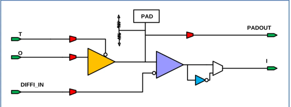
IOBs are group of basic elements that are used to implement the input and output functions of an FPGA device. The IOBs make the FPGA core accessible for the user for monitoring and measurement purposes. Figure 1-14 shows the IOB model for Xilinx Virtex FPGAs extracted by
Slice register D Q 0 1 SEU CLK 0 erroneous data
Figure 1-13 : Fault model in slice register due to SEU effect
PAD T O DIFFI_IN PADOUT I
Xilinx FPGA Editor tool [28]. It is noted that in most cases, an SEU breaks the IO circuitry and ceases the signal transmission to the output pads. As experimentally observed in [36] it may also generate DCs, while the top side of the FPGA is exposed to proton radiation. Toward the characterization of DCs in IOBs, it is conjectured that the SEU may alter the IO drive/standard of IOBs.
1.5 AVIO-403 Project
The AVIO-403 project was a team research work on the effect of cosmic rays on aircraft electronic devices and development of mitigation methods to reduce the on-board electronics’ downtime. Researchers from four academic institutions namely, Polytechnique Montréal, École de Technologie Supérieure (ÉTS), Université du Québec à Montréal (UQAM) and Concordia University were part of the team. Also, three industrial partners, Bombardier Aerospace, Canadian Space Agency (CSA), and MDA Corporation, were participating and funding the project partially. Several students were involved in this project, including three master’s and seven Ph.D. students as well as internship programs provided to undergraduate students.
The main objective of AVIO-403 project was to provide a better understanding of cosmic radiation effects on electronic systems with an emphasis on SRAM-based FPGAs. The objectives include the qualification and quantification of radiation effects along with means for prediction and mitigation of these effects. By adapting conventional design and integration techniques of embedded systems to consider the cosmic radiation effects on the functionality and reliability of electronic modules, the following key objectives were guided the research [37] :
a. The definition and implementation of an early assessment technique for high level digital design implemented into the FPGAs.
b. The definition and implementation of a verification technique for different levels of abstraction in order to simulate the faults induced by radiation.
c. The definition of a design approach in order to facilitate the pre-certification tests for radiation tolerance.
d. The investigation of fault-tolerant techniques employed in complex industrial systems.
1.6 EPICEA Project
Composite Electrical Aircraft (EPICEA) project is a team research work that has a very wide scope including the study of electromagnetic waves’ effect on aircraft, and cosmic rays effect on avionic systems that covers more objectives.
This three-year European-Canadian joint research project will address numerous avionic engineering design issues in the development of future aircrafts, aiming at a significant reduction of energy consumption through more electrical aircraft and systems integration. To be more specific, this research will release, validate and verify a unique computer-modeling platform assimilating a complete understanding of electromagnetic (EM) issues on composite electric aircraft (CEA). This includes the analysis and characterization of EM coupling, interconnections, and cosmic radiations on electrical systems together with new concepts of antennas designed to maintain performance in composite environment without modifying aircraft aerodynamics. The targeted computer platform will support a decision-making process for selection of the best strategy for the integration of electrical systems. This project will also create a more robust EM protection for electrical systems, i.e., lightweight and cost effective, a lighter and safer electrical system architecture for EM protected, less redundant, safety compliant, easy to maintain systems, a less drag on new systems of antenna while maintaining EM performance, and also will point to best possible health monitoring solutions. The research outcome will limit the recourse for over conservative protection and unnecessary redundancy in architecture design. This will overcome the weight penalty currently jeopardizing the development of energy-efficient CEAs and will strengthen the aircraft safety. The anticipated activities create a great example of Canadian international collaborative research. It attracts, involves and trains numerous highly qualified personnel for emerging CEA development. Research expertise and novel knowledge generated by this project not only enhance Canadian research profile and spur corporate growth, but have an impact on our daily life. The project focuses on emerging market needs, and timely addresses worldwide challenges. This promotes a sustainable development of Canadian society.
1.7 Problem Definition
Almost 98% of all memory elements in SRAM-based FPGAs are configuration bits, of which 90% and more control the routing resources. FPGAs are used in avionic industry and it is desired to come up with robust implemented designs against SEU. Once an SEU strikes the configuration bit of a routing interconnection, an extra delay may be induced by creating a short between a
![Figure 1-3 : SEU and MBU in the sequential logic and SET in the combinational logic [5]](https://thumb-eu.123doks.com/thumbv2/123doknet/2328105.30972/33.918.140.785.117.416/figure-seu-mbu-sequential-logic-set-combinational-logic.webp)
![Figure 1-6 : Slice architecture in Xilinx Virtex-5 FPGA [24]](https://thumb-eu.123doks.com/thumbv2/123doknet/2328105.30972/36.918.213.707.272.1012/figure-slice-architecture-in-xilinx-virtex-fpga.webp)
![Figure 1-9 : Fault models for buffers due to an injected SEU [33]](https://thumb-eu.123doks.com/thumbv2/123doknet/2328105.30972/40.918.193.726.109.633/figure-fault-models-buffers-due-to-injected-seu.webp)
![Figure 1-10 : Fault model for multiplexer due to an injected SEU [33]](https://thumb-eu.123doks.com/thumbv2/123doknet/2328105.30972/41.918.109.790.111.333/figure-fault-model-multiplexer-due-to-injected-seu.webp)
![Figure 2-3 : Simplified view of the bit flip impact on an implemented 2-input AND gate : (A) Fault free implementation, (B) an open case, (C) a short case, and (D) a delay case [32]](https://thumb-eu.123doks.com/thumbv2/123doknet/2328105.30972/57.918.110.810.109.517/figure-simplified-impact-implemented-input-fault-implementation-delay.webp)
![Figure 2-14 shows the implementation of time-domain majority voter in [110]](https://thumb-eu.123doks.com/thumbv2/123doknet/2328105.30972/75.918.233.691.101.675/figure-shows-implementation-time-domain-majority-voter.webp)
![Figure 2-14 : Digital circuit implementation of time-domain majority voter; with delayed clock signals (A), and with delayed output signal (B) [110]](https://thumb-eu.123doks.com/thumbv2/123doknet/2328105.30972/76.918.113.800.111.463/figure-digital-circuit-implementation-majority-delayed-signals-delayed.webp)
![Figure 2-15 : Time dilation flip-flop for error detection and correction studied in [113]](https://thumb-eu.123doks.com/thumbv2/123doknet/2328105.30972/77.918.160.756.111.412/figure-time-dilation-flip-error-detection-correction-studied.webp)
![Figure 3-1 : Experimental setup used by AVIO403 team at TRIUMF to measure extra delays [32]](https://thumb-eu.123doks.com/thumbv2/123doknet/2328105.30972/87.918.114.806.111.522/figure-experimental-setup-avio-triumf-measure-extra-delays.webp)