HAL Id: hal-01400418
https://hal.inria.fr/hal-01400418v2
Submitted on 10 Jan 2017
HAL is a multi-disciplinary open access
archive for the deposit and dissemination of
sci-entific research documents, whether they are
pub-lished or not. The documents may come from
teaching and research institutions in France or
abroad, or from public or private research centers.
L’archive ouverte pluridisciplinaire HAL, est
destinée au dépôt et à la diffusion de documents
scientifiques de niveau recherche, publiés ou non,
émanant des établissements d’enseignement et de
recherche français ou étrangers, des laboratoires
publics ou privés.
Architecture exploration of multi-source energy
harvester for IoT nodes
Philip-Dylan Gleonec, Jeremy Ardouin, Matthieu Gautier, Olivier Berder
To cite this version:
Philip-Dylan Gleonec, Jeremy Ardouin, Matthieu Gautier, Olivier Berder. Architecture exploration
of multi-source energy harvester for IoT nodes. IEEE Online Conference on Green
Communica-tions (Online GreenComm 2016), Nov 2016, n/a, United States. pp.27 - 32,
�10.1109/OnlineGreen-Com.2016.7805402�. �hal-01400418v2�
Architecture Exploration of Multi-source Energy
Harvester for IoT nodes
Philip-Dylan Gleonec
Wi6labs / University de Rennes 1, IRISA 10 Rue de Jouanet, ePark
35700 Rennes
Jeremy Ardouin
Wi6labs
10 Rue de Jouanet, ePark 35700 Rennes [email protected]
Matthieu Gautier and Olivier Berder
University de Rennes 1, IRISA IRISA-ENSSAT, 6 rue Kerampont
F-22305 Lannion Cedex
[email protected], [email protected]
Abstract— Wireless sensor networks are constrained by their energy supply. In order to relief this constraint, scavenging ambient energy from the environment has been considered. However, most existing energy harvesting devices rely on a single energy source, potentially reducing the sensor reliability. In this paper, we present an architecture for multi-source energy harvesting, aimed at low cost and easy integration with existing wireless sensors. Unlike existing architectures, our solution relies on a single power conditioning block. This block is powered by multiple sources, selected through a switch matrix by a dedicated controller. A prototype has been developed, validated and compared with alternative architectures. First results show our architecture benefits for systems using many heterogeneous sources, and highlights improvement possibilities through the addition of MPPT (Maximum Power Point Tracking) circuitry.
I. INTRODUCTION
Driven by the trend of the Internet of Things (IoT) and the uninterrupted demand for Machine-to-Machine applications, Wireless Sensor Network (WSN) has become an important research area for both academic and industrial worlds. In particular, sensor power efficiency is a particular concern when deploying WSNs, in order to increase their life-cycle and/or their Quality of Service (QoS). Moreover, wireless sensor nodes are heavily cost-constrained. In order to reduce development cost, designers need to rely on flexible and reusable platforms.
Most of the current sensor nodes are powered by batteries, which limits their available energy. In order to save power, most nodes use duty cycling technique: the device is kept in a low power mode most of the time, and only wakes up for a short time when required. A trade-off has to be made between autonomy and QoS, to define the time between two consecutive wake-ups [1]. In order to further increase the QoS of energy-constrained nodes, increasing the available energy with ambient energy harvesting has been considered [2].
A node using energy harvesting classically harvests power from a single energy source, e.g. wind, vibration. . . A power conditioning block transforms the harvested power in a voltage suitable to charge a battery and power the node. This power conditioning block has to be adapted to the energy source, and can be either a DC/DC voltage converter for continuous current sources such as solar panels or an AC/DC voltage converter for alternative current sources such as wind turbines.
In order to increase the harvested power, one can increase the efficiency of the power conversion or use multiple con-current energy harvesting devices. In multi-sources energy harvesting devices, the node is powered by a battery that is recharged from multiple heterogeneous sources. To this aim, [3] proposes a circuit which shares a common voltage converter between multiple harvesting sources. Switches are used to sequentially select each source during a time slot that depends on the source capabilities. However, this approach uses dedicated ASIC implementation, which can not be reused, and is too costly for our design constraints. [4] is one of the reference implementations for multi-source energy harvesting sensors. Each energy source has its own DC/DC converter and Maximum Power Point Tracking (MPPT) circuit in order to maximize efficiency. Each source stores its energy in a capacitor, and all capacitors are connected with diodes to form a reservoir capacitor array. Likewise, [5] uses multiple energy harvesting systems with their own converter to charge a common battery. Each converter is only activated when enough power is harvested. This information is sent to the node, enabling the estimation of the harvested power. In a sim-ilar manner, [6] uses multiple energy harvesting and storage modules, with plug-and-play detection based on IEEE 1451.4-2004 standard. All these works share the drawback of requiring a dedicated power conditioning circuit by energy harvesting source, thus multiplying the cost and board space required by the solution.
In this paper, we propose a multi-source energy harvest-ing architecture, which aims for a low cost and flexible implementation with existing energy harvesting devices. The solution relies on a circuit switching between energy sources. Harvested energy is stored in buffers, which are connected to a generic power conditioning block through a switch matrix. A controller is used to decide which energy source should be connected to the power block. Unlike previously described solutions, the proposed architecture uses a single generic power conditioning block to reduce the platform cost. The platform is compatible with multiple energy sources and ex-isting sensor nodes and enables implementation of intelligent control algorithms. To validate the proposed approach, our solution has been implemented on a commercial and deployed platform, and compared with a state-of-the-art system that uses
one power conditioning block for each source.
The rest of the paper is organized as follows. Section II describes the proposed switching system and gives the design choices for each part of the system. Section III presents a prototype implementation of our architecture, its power con-sumption measurements, and shows its benefits when powering a LoRaWAN-based platform. Finally, this paper is concluded in Section IV.
II. MULTIPLE SOURCES SWITCHING SYSTEM
A. System architecture
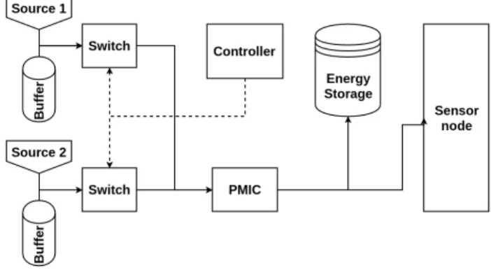
This section introduces the global design of a modular platform to which multiple energy harvesting devices can be connected. The proposed solution must keep a reasonable cost and must use available Components Off-The-Shelf (COTS) in order to ease industrialization. Moreover, this solution should be flexible enough to be associated with multiple wireless sensor platforms. Fig. 1 shows the block diagram of the proposed multi-source switching system. Each energy harvesting source is connected to a capacitor, which acts as an energy buffer while the source is not in use. Each energy buffer is connected to a central Power Management Integrated Component (PMIC) through an electrically-controlled switch. When an energy buffer is connected to the PMIC, the latter will draw as much current as it can to charge the energy storage and to power the sensor. The energy buffer is thus emptied and another one can be selected through the switch matrix to power the PMIC. A smart controller is used to decide which switch should be closed at each moment.
One of the main limitations of this architecture is that the power path contains two following DC/DC converters, which reduces the overall efficiency of energy conversion. The first one, embedded in the PMIC, is used to transform the input voltage and to charge the battery, while the second, which is part of the sensor node, takes energy from the battery to power the node components. However, this design choice allows to easily associate our system to existing sensor nodes, simply by connecting the PMIC energy storage instead of the node one.
Each function block of the architecture has multiple possible implementations, each one coming with their advantages and
Fig. 1: Multiple source switching system.
limitations. The use of capacitors is the only considered implementation for energy buffers. The following subsections detail the role and possible implementations of each main block: PMIC, switches and controller.
B. Power conditioning block
The PMIC is the power manager of the platform. Its main role is to transform the incoming energy in a suitable voltage in order to charge the energy storage (super-capacitor or battery). Implementation can be done with discrete components, using separated circuits for voltage conversion, battery charging and Maximum Power Point Tracking (MPPT). Another alternative is to use an Integrated Circuit (IC), which integrates all these functions on a single chip.
Each energy harvesting source has an optimal operating point, called Maximum Power Point (MPP), expressed as the operating voltage VM P P for which the harvested power is
maximized. In order to maximize harvesting efficiency, the converter must keep its input voltage close to VM P P. As
VM P P is a constant fraction of the harvester open-circuit
volt-age VOC, a commonly used MPPT technique is to periodically
open the circuit to let the harvester reach its VOC and to
set VM P P according to the measure of VOC. The converter
switching frequency is then adjusted to match the input voltage to VM P P.
In the proposed system, this MPPT technique can not be used. Indeed, when the circuit is opened, the input voltage of the PMIC does not reach VOC, due to the capacitance of the
energy buffers, and VM P P is therefore incorrectly measured.
Nevertheless, an external voltage VM P P can be used and set
to an arbitrary reference voltage VREF. The PMIC will then
adapt its DC/DC switching frequency to keep its input voltage close to VREF. This external control of PMIC can be used by
the controller to manage the threshold of the energy buffers.
C. Switch design
Switching between energy sources is a well-known issue. Power ORing has been used for a long time in applications where power failures are unacceptable [7], such as datacenters. However, these systems are designed for power consumption of several kW, whereas our application uses only a few mW at most. Our architecture also requires switches with no current returns in order not to damage the harvesters.
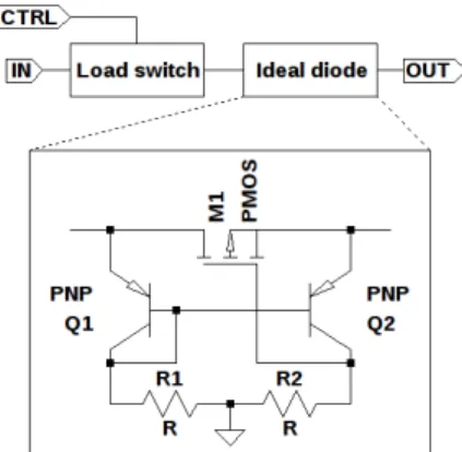
In our system, an integrated load switch is used, coupled with an ideal diode circuit to avoid reverse current flow. The switch block diagram is shown in Fig. 2. When the output voltage VOU T is lower than the input voltage VIN, Q2 PNP
transistor will be in blocking state and the FET gate voltage will be 0 V, making it passing. When VOU T is higher than
VIN, Q2 is saturated, the gate voltage is close to VOU T and
the FET is blocking. The use of two resistors to polarize the PNP transistors creates an additional power consumption. This consumption can be reduced by increasing the resistor values, however the transient response of the circuit will also increase.
Fig. 2: Load switch block diagram and schematic of the ideal diode circuit.
D. Controller implementation
In the system, the controller aims at performing the switch-ing process by controllswitch-ing each switch. Multiple decision algorithms can be implemented depending on the information that the controller could monitor in the system. For example, if the energy levels are known, the controller can allocate a time slot per source that is proportional to its maximum output power. However, as algorithmic considerations are out of the scope of this paper, no information is considered and a passive algorithm is used based on an individual and periodic turn-off of each switch. Each buffer is therefore connected to PMIC during a given duration TSW.
The only requirement for the controller is that the con-trol signals must be compatible with the selected switches. The controller is an always-on component, thus its power consumption must be reduced to a bare minimum. Although dedicated analogue or digital circuits could lower this power consumption, an ultra low power micro-controller will be used, allowing a good trade-off between power consumption and flexibility.
Indeed, recent micro-controllers usually offer multiple power modes. By keeping the micro-controller in a low power mode and only waking it up when needed, the average power used by the micro-controller can be kept close to its sleep mode power consumption, i.e. few µW. Since the micro-controller functionality is implemented using software, its features can be easily modified, simply by loading a new firmware.
III. ENERGY BUFFER CAPACITOR SIZING
The input energy buffers are implemented using capacitors. An accurate sizing of these capacitors is required, as an oversized capacitor would increase its leakage current [8], as well as the cost of the solution. On the other hand, an undersized capacitor would be too quickly charged by its energy harvester, leading to energy waste. In the proposed architecture, the size of the input energy buffers depends on both voltage and current provided by the harvesting device, but it also depends on the switching process (i.e. number of
harvesting devices, period TSW between two decisions, and
decision algorithm).
Let CBU F be the buffer capacitance and VBU F its voltage,
the current IBU F is given by:
IBU F = CBU F
d VBU F
dt . (1) The use of a solar panel is considered, which can provide up to VOCVolts, IM AXmA and has its MPP at VM P P = α∗VOC.
At initial conditions, energy buffer is supposed to be empty with a voltage down to VREF. During charging state, once
the voltage VBU F reaches VM P P, the power provided by the
panel starts to decline. The energy buffer is thus considered to be ”charged” when its voltage rises above the VM P P voltage
of its harvester. The time tCHrequired to charge the capacitor
up to VM P P is expressed by:
tCH= CBU F
α ∗ VOC− VREF
IBU F
. (2)
As the current IBU F depends on its voltage, the worst case
is considered with IBU F = IM AX. Over-sizing the current
at IM AX leads to a shorter charging time, and thus a bigger
capacitance.
The capacitance also depends on the switching process between multiple harvesters. Considering a decision algorithm with a periodic switch between the N sources, one buffer is connected to PMIC during TSW, while being in charging
state during (N −1)TSW. Therefore, to avoid overcharging the
energy buffers in such a scheme, tCH should be greater than
or equal to (N − 1)TSW. With this constraint, the minimal
energy buffer capacitance CBU F can be computed by:
CBU F ≥
TSW ∗ (N − 1) ∗ IM AX
α ∗ VOC− VREF
. (3) Finally, a safety margin is used to prevent capacitance variations, which can occur according to ambient temperature, input voltage or chosen technology, and which can change over time. This margin can be analytically derived from the capacitor specifications.
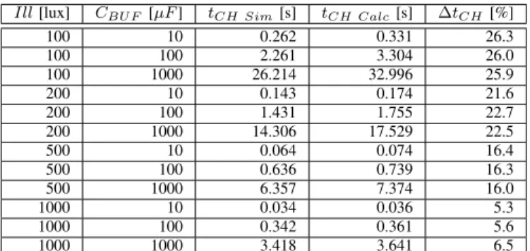
This expression has been validated through electrical sim-ulations on LTSpice, using a solar panel model as the energy source. For different capacitances and various illumination conditions, the charging time tCH Sim from VREF = 1.8 V
to VM P P is simulated, and compared with the theoretical
time tCH Calccalculated using (2). Simulation results, shown
in Table I, show that our model deviates from simulation when illuminance is low. This difference leads to oversizing the energy buffers, slighly increasing the circuit cost and leakage currents. However, it enables a simplified and sped-up capacitor sizing for each system configuration.
IV. PROTOTYPING AND MEASUREMENTS
A. Implementation
A prototype of the system presented in the previous section was developed. This implementation aims for functional vali-dation of the platform. The chosen PMIC is a SPV1050 from ST microelectronics, due to its wide input voltage range. This
Ill [lux] CBU F [µF ] tCH Sim[s] tCH Calc[s] ∆tCH[%] 100 10 0.262 0.331 26.3 100 100 2.261 3.304 26.0 100 1000 26.214 32.996 25.9 200 10 0.143 0.174 21.6 200 100 1.431 1.755 22.7 200 1000 14.306 17.529 22.5 500 10 0.064 0.074 16.4 500 100 0.636 0.739 16.3 500 1000 6.357 7.374 16.0 1000 10 0.034 0.036 5.3 1000 100 0.342 0.361 5.6 1000 1000 3.418 3.641 6.5
TABLE I: Comparison between tCHCalc and tCHSim.
IC integrates a resistor divider based MPPT circuit. Moreover, an external voltage can be applied to manually set the target operating point. If this voltage is not set, the PMIC uses MPPT circuitry, as described before.
The implemented load switch is a SiP32431 from Vishay, coupled with the ideal diode circuit described in the previous section. Due to its input voltage limitations, this circuit can only be used for energy harvesting sources providing voltage between 1.1 V and 5.5 V. For different voltages, another load switch should be used.
The controller is implemented using an MSP430FR5969 micro-controller from Texas Instruments. Its extensive power modes enable to lower the power consumption of the con-troller to few µW . Its flexible clocking trees enable the use of many peripherals while being in low power mode. In our implementation, to avoid adding an external Digital-to-Analogue Converter (DAC), an internal timer is used as a Pulse Width Modulation signal, averaged through a low-path RC filter to provide the PMIC its VREF voltage. VREF is set
to 1.1 V at minimum, to keep the energy sources voltages in the SiP32421 voltage range. A TPS60210 charge pump with ultra-low quiescent current is used to power the MSP430 with a constant 3.3 V voltage, attenuating the battery voltage variations.
B. Energy consumption overhead
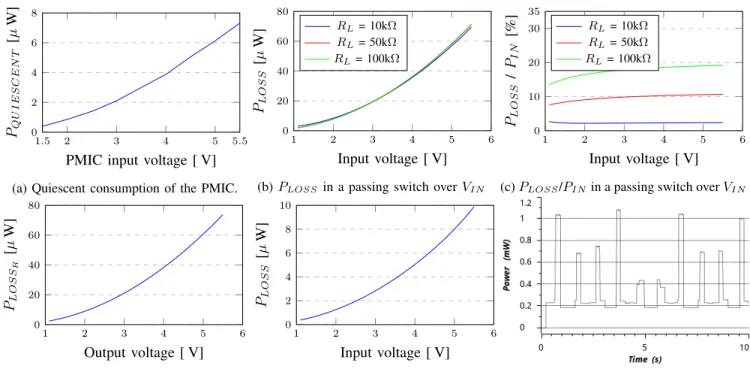
One of the main design goals for the harvester control system is to have a low power consumption in order to not disturb the node energy harvesting capabilities. Thus, we measured the system power consumption to ensure that the power consumption overhead of the proposed system is kept low. Power consumption of each block has been separately measured, and can be directly compared with the input power. The results are displayed in Fig. 3.
1) PMIC power consumption: The PMIC includes some control electronics, and thus has a quiescent current consump-tion. To measure only the power consumption overhead of our solution and not the overall conversion efficiency, the power losses due to the PMIC voltage conversion are not taken in account. The quiescent power losses are shown in Fig. 3a.
2) Load switch power losses: In order to measure the power losses PLOSS of the load switch, the output power of the
switch is subtracted to its input power PIN. Measurements
have been performed with three different load resistors RL,
for different input voltages VIN. A measurement campaign
has also been run while varying the voltage of the switch output, in order to measure its reverse leakage power losses PLOSSR.
Fig. 3b shows the raw power losses induced by the proposed load switch. In all cases, the power consumption is similar and gives a maximum loss of 74 µW for 5.5 V f. As most power losses come from the ideal diode circuit resistors, these losses are voltage dependent, and different loads have no impact. However, this also means that the power consumption overhead of the switch is proportionally higher when a lower current is flowing through, as shown in Fig. 3c. In our use-case, the current flowing through the switch is reduced when the energy buffer voltage VBU F is close to the reference voltage
VREF, i.e. when the buffer is nearly depleted.
Moreover, the switches have a reverse power leakage. These losses are due to the ideal diode resistors, and thus are close to the losses of a passing switch, as shown in Fig. 3d. Adding too many energy harvesting sources has a negative impact on total harvested power, as it increases the total reverse leakage power of the switches. In the case of a system with N energy harvesting devices, the reverse power losses are equal to (N − 1) × PLOSSR(V ).
However, these power losses only affect the currently se-lected energy harvesting source, which provides current to the PMIC. When the switch is in blocking mode, the other sources are charging their respective energy buffer. Thus, the only power losses that affect them are the leakage current of the energy buffer and the power consumption of the SiP32421 load switch. These power losses are in order of µW, as can be seen in Fig. 3e.
3) Controller power consumption: The MSP-EXP430FR5969 development platform provides an embedded energy measurement tool, enabling real-time measurement of the controller power consumption. In order to take into account the power drawn by the controller charge pump, we powered our development board from the charge pump, and powered this charge pump from the integrated debugger 3.6 V power supply. The charge pump is set in low-power mode, so that its quiescent current consumption is minimized. The State-of-Charge (SoC) of the main energy storage is measured with an external ADC with high input impedance through a resistor divider.
The controller implements a simple decision algorithm, which alternatively closes the switches each TSW = 1 s. It
also implements a simple power manager, which measures the main energy storage SoC and commands the sensor node to transmit a packet if the storage is charged. Therefore, the more energy is harvested, the lower the period between two transmissions TP T X will be.
Fig. 3f illustrates the power consumption of the controller on a 10 second period. To get the average power consumption of the full circuit, a 5 minute measurement has been run. The mean power consumption was 334 µW for a current of 92 µA. The power losses induced by the controller are relatively high,
1.5 2 3 4 5 5.5 0 2 4 6 8
PMIC input voltage [ V] PQU I E S C E N T [µ W]
(a) Quiescent consumption of the PMIC.
1 2 3 4 5 6 0 20 40 60 80 Input voltage [ V] PLO S S [µ W] RL= 10kΩ RL= 50kΩ RL= 100kΩ
(b) PLOSS in a passing switch over VIN
1 2 3 4 5 6 0 10 20 30 35 Input voltage [ V] PLO S S / PI N [%] RL= 10kΩ RL= 50kΩ RL= 100kΩ
(c) PLOSS/PIN in a passing switch over VIN
1 2 3 4 5 6 0 20 40 60 80 Output voltage [ V] PLO S SR [µ W]
(d) PLOSSRof a switch over VOU T
1 2 3 4 5 6 0 2 4 6 8 10 Input voltage [ V] PLO S S [µ W]
(e) PLOSS in a blocking switch over VIN (f) Power consumption of the controller.
Fig. 3: Power consumption overhead of the platform.
and mainly come from the ADC measurements required by the power manager. If the switch system is implemented without the power manager, the power consumption of the controller decreases at 185 µW for a current of 51 µA.
C. System validation
1) Test set-up: Our system is used to power a wireless sensor developed by Wi6labs [9]. This platform is built around a STM32 micro-controller from STmicroelectronics, and uses the LoRaWAN protocol for communications. This choice eases the estimation of the power consumption of the node. Indeed, as the LoRaWAN network has a star topology, an end-device does not have to route any message and its power consumption does not depend from the other nodes behavior.
Voltage generators are used to emulate sources. The first source is set at 4.2 V, while the second is set between 1.5 V, 3.1 V or 3.7 V. Both sources are limited to 1 mA in order to simulate low power sources. As the sources are fixed, different measurements can be performed in a consistent set-up, without influence from the environment. However, these sources are still oversized compared to real energy sources. As the power provided by real sources would be lower, the power consumption overhead of the circuit would have a higher impact on the harvested energy.
Even if these energy sources are oversized, compared to low power provided by real energy sources, the use of de-terministic sources allows an accurate characterization of the proposed system. Different measurements can be performed in a consistent set-up, without being affected by the environment. The input energy buffers used are arbitrarily chosen and have respectively a 4700 µF and 1000 µF capacitance, while
the energy storage is a capacitor array with a 34.7 mF total capacitance.
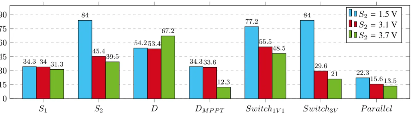
2) Measurements: The realized prototype is functional and shows that the system is able to self-start. Functionality of the controller has also been validated using a simple switch algo-rithm. In order to compare our proposal against alternatives, a prototype close to the state-of-the-art parallel architectures has been set-up. In this prototype, two PMIC SPV1050 are used in parallel, and charge the same energy storage. Both PMIC include MPPT and battery protection. The following situations are evaluated:
• S1/2: Source 1/2 only, with MPPT
• D: Source 1 and 2 connected to a single PMIC through
ideal diode circuit, without MPPT
• DM P P T: Source 1 and 2 connected to a single PMIC
through ideal diode circuit, with MPPT
• Switch1 V 1/3V: Periodic switch (TSW = 1 s) with PMIC
VREF set to 1.1 V/3.0 V
• P arallel: Parallel architecture - two PMIC directly con-nected to the battery, with MPPT.
For all situations, the period TP T Xbetween two consecutive
LoRa packet transmissions is measured ten times. The average value TP T X is then computed. These results are shown in
Fig. 4.
3) Discussion: The situation D performs significantly worse than single-source situations, while DM P P T performs
better. This is due to the lack of any MPPT in situation D, and shows the impact of MPPT. However, DM P P T is a naive
implementation, and is not efficient if the two voltages are too different. When the MPPT circuit measures VOC, it will
S1 S2 D DM P P T Switch1V 1 Switch3V P arallel 0 15 30 45 60 75 90 34.3 84 54.2 34.3 77.2 84 22.3 34 45.4 53.4 33.6 55.5 29.6 15.6 31.3 39.5 67.2 12.3 48.5 21 13.5 S2 = 1.5 V S2 = 3.1 V S2 = 3.7 V
Fig. 4: Period in s between two LoRa TX depending on situation and S2 voltage.
accordingly. Thus, a source with a lower voltage will operate far from its MPP, or will not provide power even if its voltage is smaller than the measured VM P P.
Our solution is hindered by the lack of MPPT. By setting VREF too low, as in situation Switch1 V 1, the sources operate
far from their optimal power point, and provide less energy. Alternatively, rising VREF too high may render some sources
useless. Indeed, if S1 is set at 4.2 V, rising VREF to 3 V
brings the converter operating point closer to the source MPP. But, if the second source voltage is smaller than VREF, no
current will be drawn, and the source will not be used at all. However, if VREF is close to both sources MPP, such as
situation Switch3V with S2 set a 3.7 V, our solution performs
correctly. This demonstrates the potential of our solution, when the sources operate close to their MPP.
The energy buffer size has also an impact on the system: an oversized buffer takes more time to charge, and the energy source takes a longer time to reach its VM P P. In order to
maximize harvesting efficiency, decision algorithms should be designed so that the sources operate near their MPP. Possible solutions include setting VREF from a DAC and adapt its value
according to the selected source, or adding a full-featured MPPT circuit between a source and its energy buffer.
Cost was a primary concern when designing our system. Table II shows the cost associated with a state-of-the-art par-allel architecture and our switching architecture. Only active components are taken in account. Prices are obtained from standard distributors for 100 pieces of each component. Ideal diode cost is estimated. N designates the number of harvesters in the system. Our system becomes cost effective for N ≥ 3, which makes it interesting for systems using a large number of energy sources.
Component Switching Arch. Parallel Arch. Name Unit Price Count Price Count Cost SPV1050 $2.21 1 $2.21 N $N × 2.21 MSP430 $0.70 1 $0.70 0 $0 TPS60210 $1.47 1 $1.47 0 $0 SiP32431 $0.28 N $N × 0.28 0 $0 Ideal diode $0.30 N $N × 0.30 0 $0 Total 1 $(4.38 + N × 0.58) 1 $N × 2.21
TABLE II: Cost breakdown of the solution.
V. CONCLUSION
This paper describes a multi-source energy harvesting ar-chitecture, where multiple energy sources are multiplexed into a single PMIC through a switch matrix. The use of a single voltage converter enables to lower the cost of the solution. The system was validated with a LoRa wireless sensor platform and its power consumption overhead was measured. Measurements show that our solution can efficiently power a node from multiple energy sources, when all sources operate close to their MPP. Future work will focus on adding ultra low power MPPT circuits to keep each source close to its MPP, thus maximizing harvesting efficiency for each source, while not adding too much cost. The simplification of the controller implementation will also lower the cost of the platform.
REFERENCES
[1] O. Sentieys, O. Berder, P. Qu´emerais, and M. Cartron, “Wake-Up Inter-val Optimization for Sensor Networks with Rendez-vous Schemes,” in Workshop on Design and Architectures for Signal and Image Processing (DASIP), Nov. 2007.
[2] C.-Y. Chen and P. H. Chou, “DuraCap: A supercapacitor-based, power-bootstrapping, maximum power point tracking energy-harvesting system,” in Proc. 16th ACM/IEEE International Symposium on Low Power Elec-tronics and Design (ISLPED), pp. 313–318, Aug. 2010.
[3] S. Bandyopadhyay and A. P. Chandrakasan, “Platform Architecture for Solar, Thermal, and Vibration Energy Combining With MPPT and Single Inductor,” IEEE Journal of Solid-State Circuits, vol. 47, pp. 2199–2215, Sep. 2012.
[4] C. Park and P. Chou, “AmbiMax: Autonomous Energy Harvesting Plat-form for Multi-Supply Wireless Sensor Nodes,” in Proc. 3rd Annual IEEE Communications Society on Sensor and Ad Hoc Communications and Networks, vol. 1, pp. 168–177, Sept. 2006.
[5] R. Morais, S. G. Matos, M. A. Fernandes, A. L. Valente, S. F. Soares, P. Ferreira, and M. Reis, “Sun, wind and water flow as energy supply for small stationary data acquisition platforms,” Computers and Electronics in Agriculture, vol. 64, pp. 120–132, Dec. 2008.
[6] A. S. Weddell, N. J. Grabham, N. R. Harris, and N. M. White, “Mod-ular Plug-and-Play Power Resources for Energy-Aware Wireless Sensor Nodes,” in Proc. 6th Annual IEEE Communications Society Conference on Sensor, Mesh and Ad Hoc Communications and Networks, pp. 1–9, Jun. 2009.
[7] R. White, “Using Redundant DC Power in High Availability Systems,” in IEEE Applied Power Electronics Conference and Exposition (APEC), pp. 848–853, Mar. 2006.
[8] T. Zhu, Z. Zhong, Y. Gu, T. He, and Z.-L. Zhang, “Leakage-aware energy synchronization for wireless sensor networks,” in Proc. 7th ACM International Conference on Mobile Systems, Applications and Services, pp. 319–332, Jun. 2009.
[9] Wi6labs, “Wi6labs LoRa platform.” http://www.wi6labs.com/ lora/, 2016. [Online; accessed 10-May-2016].