HAL Id: tel-01310585
https://pastel.archives-ouvertes.fr/tel-01310585
Submitted on 2 May 2016HAL is a multi-disciplinary open access archive for the deposit and dissemination of sci-entific research documents, whether they are pub-lished or not. The documents may come from teaching and research institutions in France or abroad, or from public or private research centers.
L’archive ouverte pluridisciplinaire HAL, est destinée au dépôt et à la diffusion de documents scientifiques de niveau recherche, publiés ou non, émanant des établissements d’enseignement et de recherche français ou étrangers, des laboratoires publics ou privés.
STUDY OF IN-PLANE SILICON NANOWIRES
OBTAINED VIA A SOLID-LIQUID-SOLID GROWTH
PROCESS AND THEIR SELF- ORGANIZATION FOR
ELECTRONIC APPLICATIONS
Zheng Fan
To cite this version:
Zheng Fan. STUDY OF IN-PLANE SILICON NANOWIRES OBTAINED VIA A SOLID-LIQUID-SOLID GROWTH PROCESS AND THEIR SELF- ORGANIZATION FOR ELECTRONIC APPLI-CATIONS. Materials Science [cond-mat.mtrl-sci]. Ecole Polytechnique, 2015. English. �tel-01310585�
D
OCTORALT
HESIS INP
HYSCIS(M
ATERIALS
CIENCE)
S
TUDY OF IN
-
PLANE SILICON NANOWIRES OBTAINED VIA A
SOLID
-
LIQUID
-
SOLID GROWTH PROCESS AND THEIR SELF
-ORGANIZATION FOR ELECTRONIC APPLICATIONS
Thèse présentée en vue d‟obtenir le grade de
Docteur de l'École Polytechnique
Spécialité Physique / Science des Matériaux
par
FAN
Z
HENGS
TUDY OF IN
-
PLANE SILICON NANOWIRES OBTAINED VIA A
SOLID
-
LIQUID
-
SOLID GROWTH PROCESS AND THEIR SELF
-ORGANIZATION FOR ELECTRONIC APPLICATIONS
Soutenue le 21décembre
2015 à l‟Amphi Becquerel devant le jury composé de :P
ROF.
P
EREROURA
GRABULOSA
UDG
Rapporteur
D
R.
F
RANKGLAS
LPN
Rapporteur
D
R.
F
RANCKFORTUNA
CSNSM
Examinateur
D
R.
S
OPHIEBOUCHOULE
LPN
Examinateur
à mes chers parents et Nan
A
CKNOWLEDGEMENTS
This Ph.D. work is in collaboration with Laboratoire de Photonique et de Nanostructures (LPN), and is partially supported by the scholarship from Chinese Scholarship Council (CSC), FX-conseil and the facilities from Réseau National des Grandes Centrales de Technologies (RENATECH). I appreciate the fruitful discussion and comments from my jury members: Dr. Pere Roura Grabulosa, Dr. Frank Glas, Dr. Franck Fortuna and Dr. Sophie Bouchoule.
All started from the summer 2012, when my Ph.D. subject of CSC-Groupe d‟Ecole Centrale was administratively cancelled and I was busy looking for an alternative one in a French lab. It seemed to be quite late and most of the posted theses were not available anymore at that time. After throwing a large amount of application e-mails into the internet, I received a less negative response from Prof. Pere Roca i Cabarrocas in Laboratoire de Physique des Interfaces et des Couches Minces (LPICM, Ecole Polytechnique). No surprising on the regretting phrases, however, in the attachment there was another Ph.D. proposal on in-plane solid-liquid-solid silicon nanowireTM, and one Phys. Rev. Lett. . I had never heard of nanowires, neither the Phys. Rev. Lett. However, a huge
amount of technologies were listed in the proposal: PECVD, sputtering, evaporation, lithography, plasma etching, SEM, as well as transistor fabrication and electrical characterization, etc. So, I decided to come. Thank you Prof. Yu for the phone interview and for introducing such a amazing and chanllenging Ph.D. subject.
It is my honor to have a three-year Ph.D. study in LPICM, where I meet so many talented researchers, engineers and Ph.D. students. I would like to say Merci Jacqueline for the training on SEM, Raman AFM, and Ellipsometer Spectroscopy. Merci Nada and Jean-Christophe for the Raman training on Total side. Merci Cyril, Pavel, Dmitri and Garry for the PLASFIL maintainence, without your support I can not finish my Ph.D. in time. Merci Jérôme, Frédéric from l‟équipe du BEER for the facility maintainence and other various tiny things like cutting corning glass, providing screws and printing posters. Merci Fouad and Isabelle from PMC for the SEM maintainence. Merci Erik, Jean-Eric, Ileana, Antonin, Wanghua for attending my oral presentation rehearsal and providing valuable advices. Merci all the silicon nanowire group members: Aliénor, Zuzana, Soumyadeep, Jian, Ben, especially to Martin for organising our group. Merci Denis, I owe you an expensive shadow mask! Merci beaucoup to Jean-Luc for the TEM studies on indium nanoparticles, ITO thin films and in-situ TEM observation of in-plane silicon nanowire growth, also merci beaucoup for your patience during the last two years, and merci beaucoup for the seminar organisation with your elegant French in e-mails. Merci Romain for the discussions on epitaxy and the kind help on ellipsometry characterization. Merci Junkang for the discussions on µc-Si deposition and ellipsometry modelling as well as Raman characterization. Futhermore, merci Laurence, Carine et toutes les secrétaires for all the paperworks like la demande de badge, les contrats, le titre de séjour, les ordres de la mission, etc. Merci Eric and Frédéric pour la service informatique. Merci beaucoup Dezeng and
ii
Yachun for helping me prepare the pot after my Ph.D. defense. Gràcies Alba for your delicious cookies, beautiful Charistmas card and your encouragement since I started the thesis writing, really hard at that time. Merci beaucoup Sang-Hyuk and Enric for taking me a ride when the transport circulation in campus was inconvenient. In the end, merci and bon courage to all the people in LPICM.
Nothing was easy. Finally, I got the badge to the Salle Blanche (SB) in LPN in July 2013. This was an entirely novel experience in my life. People were wearing blouse and gloves. People were moving fast (but not running) among the sections in SB. People were waiting in line for the equipments. Firstly, I would like to say Merci Luc for the general training before getting access to SB. Merci Christophe Roblin, Christophe Dupuis and Jean-Claude for the optical lithography training, maintenance and technical support. Merci Laurent for metallization support, nice titanium/gold film and stable indium evaporation during the last two years. Merci Xavier for the dielectric sputtering coater training, maintenance and the personalized program for ITO. Merci Stéphane (Senior Guilet) for RIE and RIBE training, maintenance and the numerous discussions during the last two years, plasma etching is really a magic tool. Merci Edmond for the electron beam lithography and the discussions on our project, indium small pads did help us a lot for understanding the nanowire growth, also for the metal contact patterning for electrical characterization, quite a huge work and I really had the sensation that research should be straightforward, however, sorry for the ITO small pads that for the moment I cannot give a clear conclusion about that. Merci Kamel for the training of rapid thermal annealing (RTA), thermal oxidation and electrical characterization, really sorry that I used the RTA in a dangerous way, I will shift to a reliable way to anneal ITO, this is a very crucial process. Merci Xuan and Li for your talent ideas on nano-fabrication technologies. Merci Quan and Yong for all your educations on transistor fundamentals and technologies. Merci Guillaume, Anne-Claire, Christian, Fabrice, Lina, Andrea and all the people who helped me during the last two years in LPN. In the end, I would like to deliver my Grand Remercie to Sophie, to be short and straightforward: you are the example, I am trying to approach.
Then, I would like to talk about my thesis director. Moltes Gràcies to Pere, for your patience and encourage when I was in difficult situations, for the freedom you offered to me for the research, for all the discussions early in the morning, late in the evening and especially during the weekends and les fêtes, for the extension funding when my negotiations with CSC failed (TOOOO PITY), for the barbecues in your garden, etc. It is really luck and honorable to work with you for the last three years. Moltes Gràcies!!!
Also, I would like to thank my friends Bingrui, Hui, Ming, and ma belle Nan, with whom I enjoyed happy hours during the weekends and vacations. Finally, I would like to thank my parents for their permenant support.
FAN Zheng à Palaiseau 2016/04/20
Acknowledgements ... i
Introduction ... 1
Nano-scale semiconductors ... 1
More Moore and More-than-Moore ... 1
Strain engineering ... 3
High-k dielectrics and Metal gates ... 3
Planar vs. Non-planar architectures ... 4
Contribution of one-dimensional semiconductors to More Moore ... 5
Contribution of one-dimensional semiconductors to More-than-Moore ... 7
Fabrication and integration of one-dimensional semiconductors ... 8
Thesis structure ... 8
References ... 9
1
Fundamentals and Experimental Techniques ... 13
1.1 In-plane silicon nanowires via a solid-liquid-solid growth mode ... 15
1.2 Thin film deposition and characterization ... 19
1.2.1 Plasma-enhanced chemical vapour deposition (PECVD) ... 19
1.2.2 Sputtering ... 21 1.2.3 Thermal evaporation ... 23 1.2.4 Raman spectroscopy ... 23 1.2.5 Spectroscopic Ellipsometry ... 26 1.3 Lithography ... 33 1.3.1 Optical lithography ... 33 1.3.2 Electron-beam lithography ... 35 1.4 Dry etching ... 37
1.4.1 Reactive ion etching ... 38
1.4.2 Reactive ion beam etching ... 39
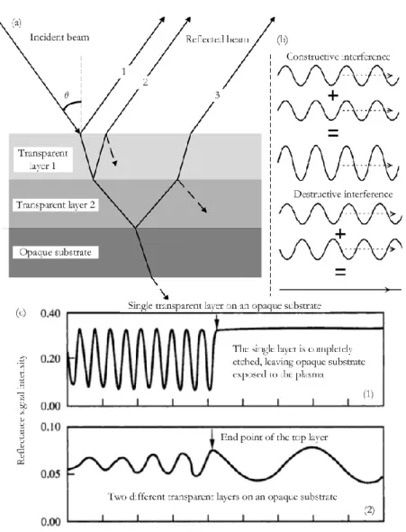
1.4.3 Endpoint detection techniques ... 40
1.4.3.1 Laser interferometry ... 40
1.4.3.2 Mass spectrometry ... 42
1.5 Electron microscopy ... 43
1.6 Summary ... 43
1.7 References ... 45
2
Indium Catalyst: from Thin Film to Nanoparticles ... 47
2.1 Metal catalysts for growing semiconductor nanowires ... 49
2.2 Thin film growth modes ... 51
iv CONTENTS
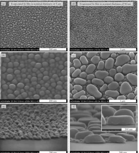
2.3.1 Microstructure of evaporated indium thin films ... 53
2.3.2 H2 plasma reduction for the a-Si:H/indium contact ... 55
2.3.3 Effect of substrate temperature on the reduction of indium oxide ... 60
2.3.4 Effects of the substrate properties on indium NPs redistribution ... 64
2.3.4.1 Indium NPs coalescing on microcrystalline Si substrates ... 64
2.3.4.2 Indium NPs coalescing on polycrystalline Al-doped ZnO substrates .. 66
2.3.4.3 Grain-boundary wetting induced coalescing mechanism ... 67
2.3.5 Conclusion ... 68
2.4 Indium nanoparticles formation on sputtered ITO thin films ... 70
2.4.1 Mechanism of indium NPs formation on ITO ... 71
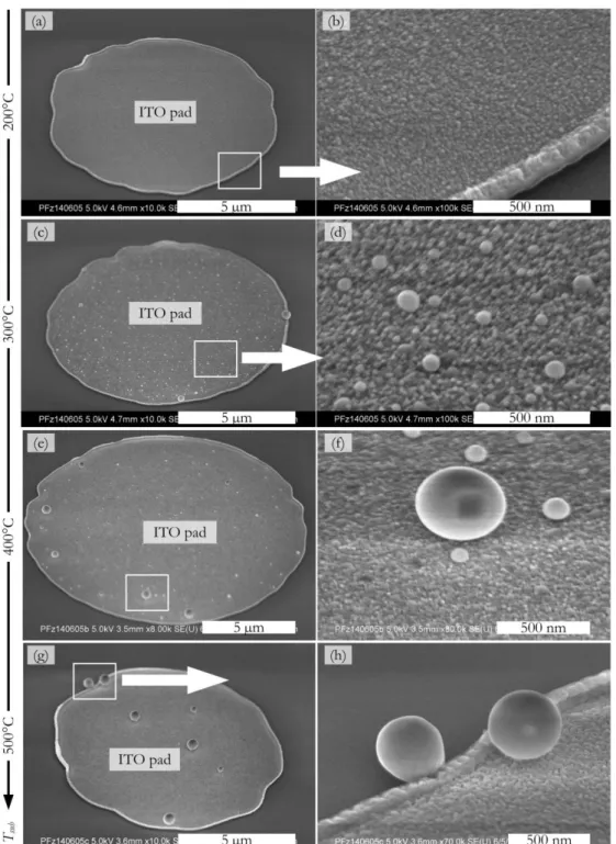
2.4.1.1 Substrate temperature dependence of indium NPs formation ... 71
2.4.1.2 Investigation of ITO surface evolution ... 73
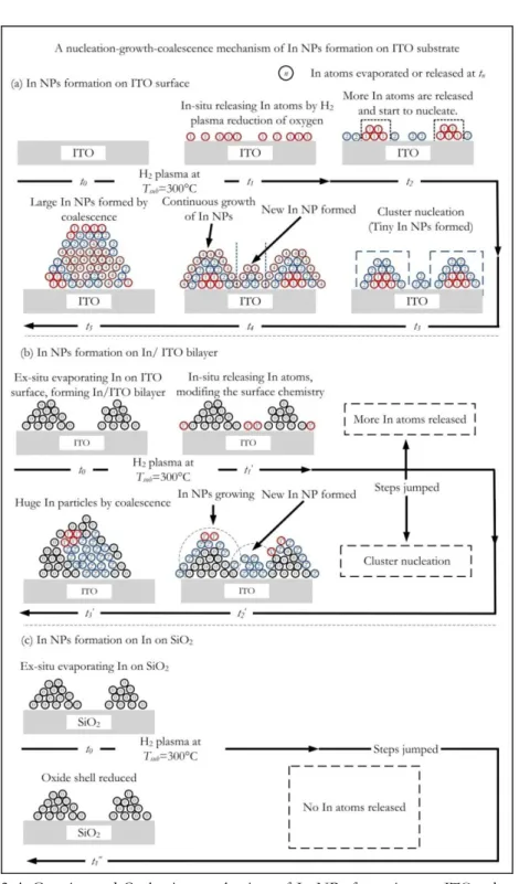
2.4.1.3 A Growth-and-Coalescence mechanism ... 76
2.4.2 Redistribution of Indium NPs on indium/ITO bilayers ... 79
2.4.3 Phase transition of ITO thin films upon heating ... 79
2.4.4 ITO reduction under various H2 plasma conditions ... 82
2.4.5 Conclusion ... 87
2.5 Summary and perspectives ... 87
2.6 References ... 89
3
Growth mechanism of In-plane Silicon Nanowires ... 95
3.1 Theoretical background ... 97
3.1.1 Metal-induced crystallization of semiconductors ... 97
3.1.2 Spontaneous motion of liquid droplets on solid surfaces ... 100
3.1.3 Heterogeneous nucleation from solution ... 103
3.1.4 Background on the In-plane SiNWs growth ... 105
3.2 Spontaneous motion of liquid Indium on a-Si:H ... 107
3.2.1 Evolution of In nanoparticles at the initial stage of SiNWs growth ... 107
3.2.1.1 Redistribution of In NPs upon their interaction with a-Si:H ... 107
3.2.1.2 Effect of a-Si:H shell on the coalescence of indium nanoparticles... 111
3.2.1.3 Investigation of µc-Si:H/In interaction ... 113
3.2.2 Large indium droplets moving on a-Si:H ... 114
3.2.3 Conclusion ... 116
3.3 Detailed analysis of the growth of Solid-Liquid-Solid SiNWs... 118
3.3.1 Setting up the IPSLS system ... 118
3.3.2 Investigation of In-plane Solid-Liquid-Solid system ... 120
3.3.3 Conclusion ... 128
3.4 Subsrate temperature dependence of a-Si:H properties ... 129
3.4.1 Activation temperature of a-Si:H/In reaction ... 129
3.4.2 Effect of a-Si:H structure on SiNW growth ... 131
3.4.3 Conclusion ... 134
3.5 Metal catalyst candidates for In-plane SiNWs Growth ... 136
3.5.1 Sn/a-Si:H interaction ... 136
3.5.4 Conclusion ... 141
3.6 IPSLS vs. VLS growth modes... 143
3.7 Summary and perspectives ... 145
3.8 References ... 147
4
Self-organisation of In-plane Silicon Nanowires ... 159
4.1 Large-scale ordered one-dimensional semiconductors ... 161
4.1.1 Growth-and-place method ... 161
4.1.2 Growth-in-place method ... 162
4.1.3 Summary ... 165
4.2 Self-organization of In-plane SiNWs ... 167
4.2.1 Step-guided growth of in-plane SiNWs ... 167
4.2.2 Positioning Indium nanoparticles on sidewalls of buried ITO matrix ... 176
4.2.3 Conclusion ... 184
4.3 Fabrication of guiding-step/buried ITO layer structure ... 186
4.3.1 Fabrication process ... 186
4.3.2 Key points in the fabrication process ... 190
4.3.3 Conclusion ... 197
4.4 Summary and perspectives ... 197
4.5 References ... 200
Summary and perspectives ... 205
N
ANO-
SCALE SEMICONDUCTORS M
OREM
OORE ANDM
ORE-
THAN-M
OOREThe method of controlling the electric currents by a three-terminal device proposed by J. E. Lilienfeld in 1930 opened the era of solid state semiconductor electronics [1], and J. S. Kilby published the miniaturized electric circuits for the first time in 1964 [2], which is nowadays known as integrated circuits (ICs) for logic devices like central computing units (CPUs) and memories, whose building blocks are based on complementary metal-oxide-semiconductor (CMOS) technology. Since then, great efforts have been made on integrating more CMOS of decreasing dimensions on a single chip, in order to keep low manufacturing cost and meanwhile maintain low power consumption with an increasing device performance, called CMOS scaling or miniaturization. During the past several decades this technology evolution was directed by the Moore‟s law (the number of transistors on a chip doubles every 18 to 24 months, as shown in Figure 1) and now currently almost approaches its limit. Novel channel materials and gate, dielectrics, supported by substrate engineering, novel device architectures with multi-gate engineering, advanced doping, as well as etching and lithography technologies are being developed for boosting the Moore‟s law, which is called “More Moore”. The evolution of corresponding technologies is summarized in Figure 2.
2 INTRODUCTION
Figure 2 Advanced CMOS technology in the transistor scaling roadmap, source from Robert Chau, Intel Corporation [4].
Moreover, semiconductor industry encounters new challenges, with the requirements of integrating non-digital (e.g. analogue) functions in a multi-functional system based on CMOS technology, including radio frequency (RF) components, power management subsystems, passive components, biochips, sensors, actuators, microelectromechanical systems (MEMS), etc. This developing direction of functional diversification is known as “More-than-Moore”. Figure 3 shows the diagram of this dual trend of More Moore (miniaturization of the digital functions) and More-than-Moore (functional diversification) from the International Technology Roadmap for Semiconductors (ITRS) [5].
Figure 3 Diagram of a dual trend of More Moore (miniaturization of the digital functions) and More-than-Moore (functional diversification) from International Technology Roadmap for Semiconductors (ITRS), from [5].
Figure 4 shows the strain engineering technolgoies that scale transistors down to the 90 nm node. Instead of introducing new materials like III-V compounds, strain engineering realizes the enhancement of device performance (electron and hole mobility) by mechanically stressing the channels (Si, Ge or SiGe alloy) of MOSFETs, including substrate-induced (or global) and process-induced (or local) technologies.
Substrate-induced strain engineering describes a process of introducing a Si1-xGex
layer between the channel layer and the substrate (normally Si), so that the top channel layer can be stretched due to its lattice mismatch with the Si1-xGex layer. Figure 4.a shows the
schematic representation of strained Si thin layer on SiGe alloy.
Another strain engineering technology is derived from the silicidation at the source and drain regions, where the channel region is stressed by the nitrides at the two sides. So it is called local or process-induced strain engineering. Later on, selective epitaxial growth of SiGe alloys embedded in the source and drain region was developed as the main technology in semiconductor industry. The advantage of local strain engineering is that the strains in P- and N- channels can be manipulated independently. Figure 4.b shows the schematic representation of process-induced strain engineering by selective epitaxial growth of SiGe alloy embedded in the source and drain regions, which forms compressive and tensile strains in p- and n- channels, respectively.
Ge Si
(b) Process-induced strain engineering (a) Substrate-induced strain engineering
Tensile strain C o m p re ss iv e st ra in SiGe alloy
Figure 4 Schematic representation of substrate-induced strain engineering (a) [6] and process-induced strain engineering (b) [7].
H
IGH-K DIELECTRICS AND M
ETAL GATESFor conventional CMOS technology, SiO2 and heavily doped polycrystalline silicon
gate are the standard materials for gate stack engineering. In the transistor scaling roadmap, the standard configuration shifts to metal gate/high-k dielectric, as shown in Figure 5.
4 INTRODUCTION
Figure 5 Schematic representation of gate stack configurations of poly-Si/SiO2 (left) and metal gate/high-k dielectric [8].
Continuous thickness reduction of SiO2 dielectrics will cause detrimental gate
leakage current. In order to obtain high device performance while maintaining low power consumption, high-k dielectrics/metal gates are introduced. High-k dielectrics are a group of metal oxides with dielectric constant k larger than 7 (the value of Si3N4). Other
requirements of high-k dielectrics are: (i) large bandgap (>5 eV) in order to establish large band offset with Si to avoid Si-dielectrics conduction due to Schottky emission of electrons and holes into the oxide bands; (ii) thermodynamic stability at the Si/dielectrics interface to avoid interfacial reaction and SiO2 formation; (iii) high thermal stability with high
crystallization temperature; (iv) high quality thin film with respect to uniformity, conformal profile and density. Commonly considered high-k dielectrics include Al2O3, HfO2, Ta2O5,
etc. The replacement of heavily doped poly-Si is due to the limitations in doping density, which result in the depletion of poly-Si gate when the gate stack is biased in inversion and lowering of the drive currents. Besides, poly-Si is not thermodynamically stable when put in contact with high-k dielectrics. Hence, metal or metal compound gates are proposed as new materials in gate stack engineering. As pure metals can react with dielectrics (e.g. Ta, Ti, Hf, etc.), while other inert ones (e.g. Ni, Pd, Pt, etc.) have difficulty in chemical bonding at metal/dielectrics interface, metallic alloys, and metal nitrides turn to be alternative materials. Metallic alloys (e.g. Ta-Pt) provide good thermal stability and adjustable work function by modulating the atomic composition fraction of two metals with different work functions. Metal nitrides, like TiN, WN, HfN, etc., are also considered as gate materials, and their work function can be tuned by the nitrogen composition. However, the range of achievable work function is not broad enough to be adaptable to both p- and n- type channels. Metal silicides are considered as the most suitable gate material as their adjustable work functions can suit both p- and n- type channels and the silicidation process (i.e. metal-Si reaction) is compatible with the CMOS technology, for example Ti silicide, Pt silicide, Ni silicide, etc.
considered as the most possible route in the More Moore roadmap. However, the competition with advanced SOI planar technology is challenging.
Planar transistor technologies can be classified as: (i) conventional bulk technology, where Si channels are formed in bulk Si; (ii) Silicon-On-Insulator (SOI) technology, where Si channels are located in the thin layer of Si (called Body) over a buried oxide insulator (called BOX) on Si substrates. If the Si Body is thicker than its depletion depth, a neutral region will exist between source and drain, called Partially-Depleted SOI (PD-SOI), the normal thickness of Si is around 50~90 nm; if the Si Body is ultra-thin, the entire layer can be depleted, called Fully-Depleted SOI (FD-SOI), the normal thickness is around 10~20 nm. In comparison with bulk Si technology, SOI has advantages like low junction capacitance and leakage, low operating power, better electrostatic control to reduce short channel effects, etc. [9]
Another competing technology, FinFET, relies on non-planar technologies for enabling the multi-gate engineering. A 3-D channel, shaped as a fin, is fabricated on bulk Si substrate, so that the gate stack layers can be coating the top and both sides of the fin channel. This dual gate architecture provides optimized electrostatic control and thus improves the current control of transistor. Besides, variant multi-gate architectures are proposed as gate engineering progresses, such as Π gate, Ω gate and even gate-all-around (GAA) [10]. However, FinFET technology encounters challenges like process complexity (e.g. uniform doping technology) and subsequent performance variation. Figure 6 shows the schematic representation of FinFET transistor (left) and FD-SOI transistor (right).
Figure 6 Schematic representation of FinFET transistor (left) and FD-SOI transistor (right) [11].
C
ONTRIBUTION OF ONE-
DIMENSIONAL SEMICONDUCTORS TOM
OREM
OORE6 INTRODUCTION
One solution for future transistors based on CMOS technology is FinFET on SOI, by combining the SOI and FinFET technologies. Silicon nanowires (SiNWs), as a type of one-dimensional (1-D) semiconductor nanostructure, are expected as an available channel candidate in this novel architecture, which can be lying on the substrate, or vertically standing on it. Figure 7 represents selected examples of SiNWFETs: (a, b) show the architecture and SEM image of a SiNW lying on SiO2 insulator, with highly doped Si
substrate as bottom gate [12]; (c, d) show the architecture and cross-sectional TEM image of junctionless SiNWFETs, where lateral flat SiNWs (or nanoribbons) are fabricated by lithography patterning and plasma etching (top-down method) on SOI substrate and highly doped by ion implantation, with a poly-Si Π gate on top [13]; (e, f) show the architecture and SEM image of a lateral SiNW suspended on a SOI substrate fabricated by a top-down method, with poly-Si gate-all-around structure [14]; (g, h) show the architecture and cross-sectional TEM image of a vertically (vapour-solid-liquid-grown) SiNW, with bottom source, top drain and gate-all-around structure [15]. Moreover, NW heterostructures broaden the range of electronic applications, core-shell heterostructures (e.g. SiGe, GaN/AlN, etc.) have been demonstrated for the high performance quantum well (QW) FET [16][17] or optoeletronics [18]. Besides SiNWs, other one-dimensional semiconductors like Ge [19], group III-V [20]-[25], III-nitride (e.g. GaN [26]), oxide (e.g. ZnO [27], SnO2 [28]) and
carbon nanotubes (CNTs) [29][30] are also explored as the channel candidates for future electronics.
Figure 7 Examples of SiNWFETs: (a) architecture of bottom gate lateral SiNWFET and the top-view SEM image (b); (c) architecture of Π gate lateral SiNWFET and the cross-sectional TEM image (d); (e) architecture of gate-all-around lateral SiNWFET and the top-view SEM image (f); (g) architecture of gate-all-around SiNWFET and the cross-sectional TEM image (h).
C
ONTRIBUTION OF ONE-
DIMENSIONAL SEMICONDUCTORS TOM
ORE-THAN
-M
OOREBesides their applications in logic electronics, 1-D semiconductors have optical, thermal, mechanical and magnetic properties, which allow their applications in photonics, biosensors, piezotronics, energy conversion and storage, etc.
Biosensors based on SiNWFETs have been reported, where the surface of a SiNW is functionalized by modifying the receptors, so that it can be recognized by the target molecules (e.g. gas, ions, proteins, DNA, etc.) through strong binding affinity. As a consequence an electrical signal arises when a biological/chemical event takes place on the surface of the channel [31]. Moreover, SiNWs can also be used in energy conversion and storage applications, like photovoltaics based on radial junction solar cells, SiNW anodes as an electrochemical energy storage material, or in thermoelectric conversion applications [32]-[34]. III-V NWs and their heterostructures have been demonstrated as novel
8 INTRODUCTION
semiconductor materials for nano-scale photodetectors, waveguides, microcavity lasers and light emitting diodes (LEDs), etc. [35][36] Moreover ZnO NWs are applied in nanogenerators, piezotronics and piezo-photonics due to their strain-induced piezopotential property [37].
F
ABRICATION AND INTEGRATION OF ONE-
DIMENSIONALSEMICONDUCTORS
In general, the methods for producing 1-D semiconductor nanostructures can be classified into two families: i) Top-down methods, based on a physical and/or chemical etching process of tailoring the bulk substrates into NWs laterally lying or vertically standing on the substrates; (ii) Bottom-up methods, which rely on growing processes catalysed or self-catalysed by collecting and organizing atomic sources (precursors) from a vapour, liquid or even solid phase, assisted by thin film deposition techniques such as chemical vapour deposition (CVD), plasma-enhanced chemical vapour deposition (PECVD), metalorganic chemical vapour deposition (MOCVD), molecular beam epitaxy (MBE), or via solution-based synthesis methods. The most popular bottom-up method is vapour-solid-liquid (VLS) growth process, based on the interaction of liquid metal droplets and atomic precursors from vapour phase and transforming them to solid crystalline phase. A variant of the VLS method is vapour-solid-solid (VSS) mode, where the metal catalysts are in solid phase. In this thesis, we will introduce another variant growth mode, called in-plane solid-liquid-solid mode [38], where liquid metal droplets (indium) move on substrates with a pre-coated layer of a-Si:H on top, absorb Si atoms from the a-Si:H layer at their advancing edge, and precipitate c-SiNW at their receding edge [39]. Numerous review articles on the growth methods and properties of semiconductor nanostructures have been published before [40]-[46], and a brief review of bottom-up growth techniques related with our growth method is presented in Chapter 2.
In order to integrate 1-D semiconductors into nano-scale systems, it is of prime importance to organise or assemble them in an efficient way. Advanced lithography techniques (e.g. e-beam lithography and nanoimprint lithography) allow the fabrication of ordered lateral and vertical 1-D semiconductor arrays via top-down method, assisted by anisotropic dry etching techniques (e.g. inductively coupled plasma reactive ion etching, reactive ion beam etching, etc.). For vertically grown 1-D semiconductor arrays, selective area epitaxial growth [47] is the most favourable way, in which the catalysts are pre-defined by the same high resolution lithography techniques. On the other hand, challenges still remain on ordering lateral arrays of 1-D semiconductors. As most 1-D semiconductors are vertically standing on the substrates, lying them down on the pre-designed positions was a most common approach in the early days, called “growth-and-place” method. Later on, the alternative “growth-in-place” method started to be considered, where the growth of semiconductor NWs or CNTs can be guided on a structured substrate with features such as nano-facets (atomic steps) or nano-channels. More information can be found in [48]. Also a brief review relating to this thesis is introduced in Chapter 4.
produced via a solid-liquid-solid (SLS) growth mode and of their self-organisation for FET application.
In Chapter 1, we first present the synthesis process of in-plane SiNWs via a solid-liquid-solid mode. Principles of thin film deposition, characterization and micro/nano fabrication technologies are also introduced.
In Chapter 2, we systematically study the formation process of indium catalyst nanoparticles: H2 plasma treatment of indium catalyst thin films on heated substrates. Two
types of catalyst source thin films are studied: (i) evaporated discontinuous In thin films, and (ii) sputtered ITO thin films. A series of experiments are designed, which reveal the different physical and chemical processes taking place on the two types of films under
ex-situ SEM observation and analysis. The deep understanding of In NPs formation is
fundamental for our stratetgy of localizing in-plane SiNWs for self-organisation.
In Chapter 3, we consider the solid-liquid-solid growth mode of in-plane SiNWs from three aspects: (i) metal-induced crystallization of amorphous silicon, (ii) spontaneous motion of liquid droplets, and (iii) heterogeneous nucleation and crystal growth from solution. By decomposing the growth process into three corresponding episodes in loop, we manage to reconstruct the entire scenario of the growth of in-plane SiNWs. Further geometric investigation of the in-plane solid-liquid-solid system under ex-situ SEM observation and analysis supports the proposed growth mechanism and reveals the relationship between SiNW diameters, In NPs diameters and a-Si:H thickness. This improvement on understanding the growth mechanism provides principles for optimizing the guided growth strategy of in-plane SiNWs. Moreover, in order to further understand the growth mechanism, the structural properties of a-Si:H and other metal catalyst candidates (Sn, Au) are investigated. This provides strategies for lowering the growth temperature and selecting metal catalysts for GeNWs, respectively.
In Chapter 4, we propose a strategy for self-organising in-plane SiNWs, which includes two aspects: (i) a guided growth method for aligning in-plane SiNWs, and (ii) a technique of forming In NPs on buried ITO sidewalls required for localizing in-plane SiNWs. Based on the mechanisms of In NPs formation on planar ITO surface and SiNWs growth on planar substrate, we elaborate the guided growth mechanism and sidewall In NPs formation mechanism, which is expected to make this self-organising strategy reproducible and reliable. Besides, the fabrication flow chart and key factors in it are elaborated.
In Appendix A, we provide the heated substrate temperature calibration of the PECVD system for SiNWs growth (PLASFIL).
10 INTRODUCTION
[1]. J. E. Lilienfeld. "Method and apparatus for controlling electric currents." US Patent 1900018 A (1930).
[2]. J. S. Kilby. "Miniaturized electronic circuits." US Patents 3138743 A (1964).
[3]. J.-P. Colinge. "Nanowire Transistors: From classical to quantum." Oral presentation in Workshop LabEx Minos, pp. 6 (2015).
[4]. R. Chau, M. Doczy, B. Doyle, S. Datta, G. Dewey, J. Kavalieros, B. Jin, M. Metz, A. Majumdar; M. Radosavljevic. "Adavanced CMOS transistors in the nanotechnology era for high-performance low-power logic applications." ICSICT, 1, 26-30 (2004).
[5]. W. Argen, M. Brillouët, P. Cogez, M. Graef, B. Huizing, R. Mahnkopf. J. Pelka, J.-U. Pfeiffer, A. Rouzaud, M. Tartagni, C. V. Hoof, J. Wagner. "Towards a More-than-Moore roadmap." Report form the CATRENE Scientific Committee, p. 12 (2011).
[6]. C. K. Maiti, T. K. Maiti. "Strain-engineered for MOSFETs." CRC Press, p. 24 (2013). [7]. V. Sverdlov. "Strain-induced effects in advanced MOSFETs." Springer, p. 10 (2011).
[8]. G. He, Z. Sun. "High-k gate dielectrics for CMOS technology." Wiley-VCH, p. XXVIII (2012).
[9]. S. A. Vitale, P. W. Wyatt, N. Checka, J. Kedzierski, C. L. Keast. "FDSOI Process Technology for Subthreshold-Operation Ultralow-Power Electronics." Proceedings of the IEEE 98(2), 333-342 (2010).
[10]. I. Ferain, C. A. Collinge, J.-P. Collinge. "Multigate transistors as the future of classical metal-oxide-semiconductor field-effect transistors." Nature 479(7373), 310-316 (2011).
[11]. A. Conley. "FinFET vs. FD-SOI: Key advantages & Disadvantages." ChipEx2014.
[12]. Y. Cui, Z. Zhong, D. Wang, W. U. Wang, C. M. Lieber. "High Performance Silicon Nanowire Field Effect Transistors." Nano Letters 3(2), 149-152 (2003).
[13]. J.-P. Colinge, C.-W. Lee, A. Afzalian, N. D. Akhavan, R. Yan, I. Ferain, P. Razavi, B. O‟Neill, A. Blake, M. White, A.-M. Kelleher, B. McCarthy, R. Murphy. "Nanowire transistors without junctions." Nat Nano 5(3): 225-229 (2010).
[14]. T. Wang, L. Lou, C. Lee. "A Junctionless Gate-All-Around Silicon Nanowire FET of High Linearity and Its Potential Applications." Electron Device Letters, IEEE 34(4): 478-480 (2013).
[15]. J. Goldberger, A. I. Hochbaum, R. Fan, P. Yang. "Silicon Vertically Integrated Nanowire Field Effect Transistors." Nano Letters 6(5): 973-977 (2006).
[16]. L. J. Lauhon, M. S. Gudiksen, D. Wang, C. M. Lieber. "Epitaxial shell and core-multishell nanowire heterostructures." Nature 420(6911): 57-61 (2002).
[17]. J. Xiang, W. Lu, Y. Hu, Y. Wu, H. Yan, C. M. Lieber. "Ge/Si nanowire heterostructures as high-performance field-effect transistors." Nature 441(7092): 489-493 (2006).
[18]. L. Rigutti, G. Jacopin, L. Largeau, E. Galopin, A. D. Bugallo, F.H. Julien, J.-C. Harmand, F. Glas, M. Tchernycheva. "Correlation of optical and structural properties of GaN/AlN core-shell nanowires." Physical Review B 83(15), 155320 (2011).
[19]. A. B. Greytak, L. L. Lauhon, M. S. Gudiksen, C. M. Lieber. "Growth and transport properties of complementary germanium nanowire field-effect transistors." Applied Physics Letters 84(21): 4176-4178 (2004).
[20]. J.-C. Harmand, F. Glas, G. Patriarche. "Growth kinetics of a single InP1-xAsx nanowire nanowire." Physical Review B 81(23): 235436 (2010).
[21]. F. Glas. "Chemical potentials for Au-assisted vapor-liquid-solid growth of III-V nanowires." Journal of Applied Physics 108(7): 073506 (2010).
[22]. D.L. Dheeraj, G. Patriarche, L. Largeau, H. L. Zhou, A.T.J. van Helvoort, F. Glas, J.-C. Harmand, B. O. Fimland, H. Weman. "Zinc blende GaAsSb nanowires grown by molecular beam epitaxy." Nanotechnology 19(27), 275605 (2008).
[23]. F. Glas, J.-C. Harmand, G. Patriarche. "Nucleation Antibunching in Catalyst-Assisted Nanowire Growth." Physical Review Letters 104(13), 135501 (2010).
Zinc Blende Semiconductors?" Physical Review Letters 99(14), 146101 (2007).
[25]. J. A. del Alamo. "Nanometre-scale electronics with III-V compound semiconductors." Nature 479(7373): 317-323 (2011).
[26]. D. Tsivion, M. Schvartzman, R. Popovitz-Biro, P. von Huth, E. Joselovich. "Guided Growth of Millimeter-Long Horizontal Nanowires with Controlled Orientations." Science 333(6045), 1003-1007 (2011).
[27]. Y. W. Heo, L. C. Tien, Y. Kwon, D. P. Norton, S. J. Pearton, B. S. Kang, F. Ren. "Depletion-mode ZnO nanowire field-effect transistor." Applied Physics Letters 85(12): 2274-2276 (2004).
[28]. E. N. Dattoli, Q. Wan, W. Guo, Y. Chen, X. Pan, W. Lu. "Fully Transparent Thin-Film Transistor Devices Based on SnO2 Nanowires." Nano Letters 7(8), 2463-2469 (2007). [29]. C. Kocabas, S.-H. Hur, A. Gaur, M. A. Meitl, M. Shim, J. A. Rogers. "Guided Growth of
Large-Scale, Horizontally Aligned Arrays of Single-Walled Carbon Nanotubes and Their Use in Thin-Film Transistors." Small 1(11): 1110-1116 (2005).
[30]. S. J. Kang, C. Kocabas, T. Ozel, M. Shim, N. Pimparkar, M. A. Alam, S. V. Rotkin, J. A. Rogers. "High-performance electronics using dense, perfectly aligned arrays of single-walled carbon nanotubes." Nat Nano 2(4), 230-236 (2007).
[31]. K.-I. Chen, B.-R. Li, Y.-T. Chen. "Silicon nanowire field-effect transistor-based biosensors for biomedical diagnosis and cellular recording investigation." Nano Today 6(2), 131-154 (2011).
[32]. A.I. Hochbaum and P. Yang. "Semiconductor Nanowires for Energy Conversion." Chemical Reviews 110(1): 527-546 (2010).
[33]. Y. Wang, T. Wang, P. Da, M. Xu, H. Wu, G. Zheng. "Silicon Nanowires for Biosensing, Energy Storage, and Conversion." Advanced Materials, 5177–5195 (2013).
[34]. S. Misra, L. Yu, W. Chen, M. Foldyna, P. Roca i Cabarrocas: “A review on plasma-assisted VLS synthesis of silicon nanowires and radial junction solar cells”. J. Phys. D: Appl. Phys. 47, 393001 (2014).
[35]. M. S. Gudiksen, L. J. Lauhon, J. Wang, D. C. Smith, C. M. Lieber. "Growth of nanowire superlattice structures for nanoscale photonics and electronics." Nature 415(6872), 617-620 (2002).
[36]. R. Yan, D. Gargas, P. Yang. "Nanowire photonics." Nat Photon 3(10): 569-576 (2009). [37]. Z. L. Wang, R. Yang, J. Zhou, Y. Qin, C. Xu, Y. Hu, S. Xu. "Lateral nanowire/nanobelt
based nanogenerators, piezotronics and piezo-phototronics." Materials Science and Engineering: R: Reports 70(3-6): 320-329 (2010).
[38]. L. Yu, P.-J. Alet, G. Picardi, P. Roca i Cabarrocas. "An In-Plane Solid-Liquid-Solid Growth Mode for Self-Avoiding Lateral Silicon Nanowires." Physical Review Letters 102(12), 125501 (2009).
[39]. L. Yu and P. R. i Cabarrocas "Growth mechanism and dynamics of in-plane solid-liquid-solid silicon nanowires." Physical Review B 81(8): 085323 (2010).
[40]. J. Hu, T. W. Odom, C. M. Lieber. "Chemistry and Physics in One Dimension: Synthesis and Properties of Nanowires and Nanotubes." Accounts of Chemical Research 32(5), 435-445 (1999).
[41]. S. T. Lee, N. Wang, C. S. Lee. "Semiconductor nanowires: synthesis, structure and properties." Materials Science and Engineering: A 286(1): 16-23 (2000).
[42]. Y. Xia, P. Yang, Y. Sun, Y. Wu, B. Mayers, B. Gates, Y. Yin, F. Kim, H. Yan. "One-Dimensional Nanostructures: Synthesis, Characterization, and Applications." Advanced Materials 15(5), 353-389 (2003).
12 INTRODUCTION
[43]. N. Wang, Y. Cai, R. Q. Zhang. "Growth of nanowires." Materials Science and Engineering: R: Reports 60(1-6), 1-51 (2008).
[44]. V. Schmidt, J. V. Wittemann, S. Senz, Ulrich, Gösele. "Silicon Nanowires: A Review on Aspects of their Growth and their Electrical Properties." Advanced Materials 21(25-26), 2681-2702 (2009).
[45]. R. Rurali. "Colloquium: Structural, electronic, and transport properties of silicon nanowires." Reviews of Modern Physics 82(1), 427-449 (2010).
[46]. N. P. Dasgupta, J. Sun, C. Liu, S. Brittman, S. C. Andrews, J. Lim, H. Gao, R. Yan, P. Yang. "25th Anniversary Article: Semiconductor Nanowires – Synthesis, Characterization, and Applications." Advanced Materials 26(14), 2137-2184 (2014).
[47]. T. Martensson, P. Carlberg, M. Borgström, L. Montelius, W. Seifert, L. Samuelson. "Nanowire Arrays Defined by Nanoimprint Lithography." Nano Letters 4(4): 699-702 (2004). [48]. M. Kwiat, S. Cohen, A. Pevzner, F. Patolsky. "Large-scale ordered 1D-nanomaterials arrays:
1
F
UNDAMENTALS AND
E
XPERIMENTAL
T
ECHNIQUES
C
ONTENTS1.1 In-plane silicon nanowires via a solid-liquid-solid growth mode ... 15 1.2 Thin film deposition and characterization ... 19 1.2.1 Plasma-enhanced chemical vapour deposition (PECVD) ... 19 1.2.2 Sputtering ... 21 1.2.3 Thermal evaporation ... 23 1.2.4 Raman spectroscopy ... 23 1.2.5 Spectroscopic Ellipsometry ... 26 1.3 Lithography ... 33 1.3.1 Optical lithography ... 33 1.3.2 Electron-beam lithography ... 35 1.4 Dry etching ... 37 1.4.1 Reactive ion etching ... 38 1.4.2 Reactive ion beam etching ... 39 1.4.3 Endpoint detection techniques ... 40 1.4.3.1 Laser interferometry ... 40 1.4.3.2 Mass spectrometry ... 42 1.5 Electron microscopy ... 43 1.6 Summary ... 43 1.7 References ... 45
GROWTH MODE
Based on thin film techniques, in-plane silicon nanowires are synthesized in PLASFIL, a PECVD system in which the plasma is ignited by applying a RF power (13.56 MHz). Figure 1.1 shows a schematic representation of the PLASFIL system. The bottom electrode is grounded and the upper electrode is connected to the RF power generator through an impedance matching box, which is used to minimize the power reflection from the plasma by equalizing the impedances of the external power source (ZRF) to that of the
plasma (Zplasma). The series connected capacitor within the impedance matching box is called
blocking capacitor, and this mode of sustaining the plasma is thus named capacitively coupled plasma (CCP). Resistive heaters are integrated with each electrode to heat them up to a nominal temperature of 600°C. The vacuum system consists of a primary oil-sealed mechanical pump for approaching low vacuum background (10-5~10-4 mbar) and with a
turbomolecular pump for high vacuum (above 5x10⁻⁶ mbar). A Pirani gauge (thermal
conductivity gauge) and a Penning gauge (ionization gauge) are integrated in the system for monitoring the low and high vacuum pressure, respectively. During the plasma process, gases are introduced from inlet lines, and non-reacted gases or volatile gaseous reactants are pumped out of the chamber. A butterfly valve is, connected between the chamber and rector pump, for adjusting the total gas pressure thanks to adaptative pressure controller. The spatial distribution of the average DC potential voltage between the two parallel electrodes is also shown in Figure 1.1.
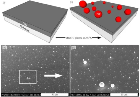
The synthesis of in-plane SiNWs is catalysed by liquid indium nanoparticles (In NPs). The source of indium (In) can be evaporated In or sputtered indium tin oxide (ITO) thin films, which experience the same process steps in PECVD system: (i) H2 plasma
treatment at 300°C, (ii) a-Si:H coating at 150°C, (iii) annealing at 450°C in vacuum or in the presence of H2. Figure 1.3 and Figure 1.4 show the flow charts and the corresponding SEM
images of the in-plane SiNWs fabrication process based on evaporated In or sputtered ITO thin films as catalyst source, respectively. The difference between evaporated In and sputtered ITO thin films is detailed in Chapter 2.
The growth of in-plane SiNWs includes the diffusion of Si atoms into liquid In NP from its front side and their precipitatation in the form of a c-Si nanowire, as illustrated in Figure 1.2. Therefore, it is a solid-liquid-solid growth process. The growth mechanism is detailed in chapter 3.
16 1.1 IN-PLANE SILICON NANOWIRES VIA A SOLID-SOLID-SOLID GROWTH MODE
Figure 1.1 Schematic representation of PLASFIL: the PECVD system for in-plane SiNWs synthesis.
Figure 1.2 Schematic representation and SEM image of in-plane SiNWs obtained via a solid-liquid-solid mode.
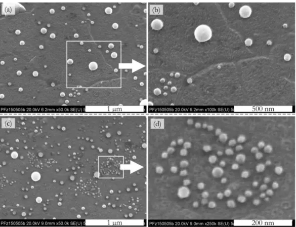
Figure 1.3 Flow chart of in-plane SiNWs synthesis with evaporated In as a catalyst source. Note that the variation of density and size of In NPs in the four images may be due to the fact that they were not taken at the same position on the same sample.
18 1.1 IN-PLANE SILICON NANOWIRES VIA A SOLID-SOLID-SOLID GROWTH MODE
Figure 1.4 Flow chart of in-plane SiNWs synthesis with sputtered ITO as a catalyst source. Note that the variation of density and size of In NPs in the four images may be due to the fact that they were not taken at the same position on the same sample.
As mentioned in 1.1, the synthesis of in-plane SiNWs is based on thin film process. In this section, the thin film deposition and characterization techniques utilized in this thesis are presented.
1.2.1 P
LASMA-
ENHANCED CHEMICAL VAPOUR DEPOSITION(PECVD)
Plasma-enhanced chemical vapour deposition (PECVD) is widely used for the growth of dielectric films (i.e. Si3N4 and SiO2) [1], a-Si:H [2], µc-Si:H [3], and c-Si epitaxy [4].The schematic representation of a RF-PECVD system has been shown in Figure 1.1. It is a sort of chemical vapour deposition (CVD) reactor, where single or mixed gaseous compounds are partially dissociated and the dissociation products (called reactive species or radicals) diffuse to the substrate and form a thin film on it due to reactive chemical process. Take silane (SiH4) in a PECVD system for instance. Radio-frequency power, as an
electrical excitation mode, provides energy to electrons which will partially ionize the SiH4
gas at a low pressure (a few tens of mTorr to a few Torr). The electrons with low mass are accelerated by the electrical field between the two parallel plate electrodes and gain enough energy to dissociate SiH4 gas via electron-molecule collisions. The products of the reaction
can be various, including positive and negative ions, radicals, electrons, photons, etc. Figure 1.5 shows the probability manifold for the SiH4 dissociative species due to a 70 eV electron
impact, deduced from mass spectrometry measurements.
At the initial stage of plasma establishment, low mass/high energy electrons are rapidly evacuated to the reactor walls leaving behind positively charged ions.This results in the formation of a space charge region where an electrical field confines the negative ions and electrons, while accelerating the positive ions (ion bombardment). The space charge region between the plasma bulk and the chamber wall has a low electron density which results in a low level of gas excitation. As a consequence it appears dark and is called sheath. The type of interaction between plasma species and the substrate depends on the charge of the species, as illustrated in Figure 1.6.
Figure 1.7 depicts the standard model of a-Si:H thin film deposition, where SiH3
radicals, as the dominant precursors at low pressure, arrive on a H-terminated surface, physisorb (as low temperature in PECVD system cannot activate the Si-H bond breaking) and diffuse on the surface to grow the film due to various chemical reactions, such as desorption of SiH3, recombination with other SiH3 to produce Si2H6 molecules, and
abstraction of H atoms to produce SiH4 molecules, which results in dangling bonds on the
surface for the following SiH3 radicals to form chemical bonds and thin film growth.
Other excitation modes can also provide energy to dissociate the gas precursors and sustain the chemical reactive system for thin film growth, like thermal or photonic activated CVD [5].
20 1.2 THIN FILM DEPOSITION AND CHARACTERIZATION
Figure 1.5 Probability manifold for the SiH4 dissociative species due to a 70 eV electron impact deduced from mass spectrometry measurements [6].
Figure 1.6 The plasma provides the source of reactive species, whose interaction with the substrate depends on their charge due to the presence of a space charge region (sheath) between the plasma and the chamber walls [7].
Figure 1.7 Standard model of a-Si:H deposition based on the interaction of SiH3 radicals with a hydrogen terminated silicon surface [7].
1.2.2 S
PUTTERINGSputtering is a physical vapour deposition (PVD) process, where the atoms are ejected from a „target‟ due to the collision of energetic ions and diffuse onto the substrate surface for the film growth. Inert gases like Ar are normally used as the sputter source, and the configuration can be glow discharge or ion beam. The glow discharge source is commonly sustained between the two parallel plate electrodes on which a DC or AC power is applied, in a similar way to the PECVD system. Figure 1.8 shows the schematic representation of a sputter coater. Moreover, in order to increase its efficiency, a magnetic field can be applied parallel to the target surface (as shown in Figure 1.9), so that in combination of electrical field, the secondary electrons in the glow discharge can be confined in a closed circuit, therefore the glow discharge bulk is kept in front of the target surface. In addition, oxide and nitride thin films can be formed via a chemical reaction process between the target material and the gas (i.e. O2 or N2) introduced in the chamber,
which is named reactive sputtering. In this thesis, a RF-magnetron sputter coater is utilized for ITO (ITO as target) and SiO2 (Si as target and O2 as reactive gas) deposition. Compared
with PECVD deposition, the film deposited via sputtering is less conformal; however, sidewall deposition still takes place, as shown in 4.3.2.2.
22 1.2 THIN FILM DEPOSITION AND CHARACTERIZATION
Figure 1.8 Schematic representation of a sputter coater [8].
Thermal evaporation is another physical vapour deposition process that utilizes Joule-effect to heat the source material (target) thanks to an electrical current passing through the crucible until it melts and evaporates in vacuum; then the material atoms in the vapour phase transport directly to the substrate and condense to form a solid phase on it. Figure 1.10 shows a schematic representation of a Joule-effect thermal evaporator. Different from PECVD and sputtering, thermal evaporation is an anisotropic deposition process, which favours the lift-off method for patterning thin films, as will be detailed in 1.3.1. In this thesis, indium thin films are deposited by thermal evaporation. Their nominal thickness is controlled thanks to a quartz crystal microbalance.
Figure 1.10 Schematic representation of a joule-effect thermal evaporator [10].
1.2.4 R
AMAN SPECTROSCOPYRaman spectroscopy is a spectroscopic technique based on the inelastic scattering of a monochromatic light by a material, which causes wavelength shifts of the light (i.e. Raman shift). The identity and properties of the material are reflected by the Raman shift and Raman spectrum, respectively.
The principle of Raman scattering is the energy change between the absorbed and re-emitted photon upon its interaction with a molecule. Note that the molecule should have polarity so that its bonds can start to vibrate and re-emit a photon after their excitation due to the interaction with incident photons. If the photon energy change is zero, the light scattering is elastic, named Rayleigh scattering, which is the most common light scattering process. If the photon loses or grains energy during this scattering process, it is called Stokes or anti-Stokes Raman scattering. Figure 1.11 illustrates the three forms of scattering
24 1.2 THIN FILM DEPOSITION AND CHARACTERIZATION
of a monochromatic light by a material. Stokes Raman scattering depicts the process by which a molecule is raised from the ground state to a virtual state and drops back to a vibrational state, so the incident photon loses energy with decreased frequency and increased wavelength. Anti-Stokes Raman scattering occurs when a molecule starts from a vibrational state to a virtual state and drops back to the ground state, therefore the incident photon gains energy with increased frequency and decreased wavelength. As the probability of initial state energy of a molecule is determined by Boltzmann distribution:
(1-1)
where E represents the state energy, κ is the Boltzmann constant and T is the absolute temperature, the amount of molecules at the ground state is much higher than the ones at vibrational states before the photon-molecule interaction, thus Stokes scattering events are more likely to occur than anti-Stokes ones. So normally Raman spectroscopy only uses the Stokes spectrum due to its greater intensity.
Figure 1.12 shows a schematic representation of a conventional Raman spectrometer. The monochromatic light from a laser is focused on the sample surface, then scattered by the sample. Most of the scattering process is Rayleigh scattering, but a small amount results into a Stokes Raman scattering, so the filter discriminates the Rayleigh scattered light and lets Raman scattered light pass. Finally, the spectrograph splits and diffracts the Raman scattered light thanks to grating and records the electrical signal by a CCD.
Figure 1.12 Schematic representation of a Raman spectroscopy set up [12].
Figure 1.13 shows the Raman shift of hydrogenated and non-hydrogenated amorphous silicon [13]. Transverse optical (TO) peak with standard wavenumber of 480 cm-1 is the main peak of amorphous silicon, whose position and full width at half maximum
(FWHM) reflect the structural disorder of the amorphous network. Figure 1.14 shows that the TO peak position of ion-implanted amorphous silicon shifts to higher wavenumbers and the FWHM decreases (i.e. broadening of the Raman spectrum), due to thermal annealing, which implies that the structural disorder degree is reduced [14]. Other peaks like transverse acoustic (TA), longitudinal optic (LO) and acoustic (LA) peaks as shown in Figure 1.13, are also determined by the structure of the amorphous silicon network, but will not be detailed here.
26 1.2 THIN FILM DEPOSITION AND CHARACTERIZATION
Figure 1.14 Annealing effect on the TO peak position (a) and its FWHM (b), for ion-implanted amorphous silicon [14].
1.2.5 S
PECTROSCOPICE
LLIPSOMETRYAnother method for thin film characterization is the UV-visible Spectroscopic Ellipsometry (SE), which is mainly used to determine film thickness and optical constants and also applied to characterize composition, crystallinity, roughness, and other material properties associated with a change in optical response.
In principle, ellipsometry measures the change of polarization of the light transmitted or reflected from a thin film. Light can be depicted as an electromagnetic wave traveling through space. Polarization is a property of wave that can oscillate with more than one orientation. Figure 1.15 illustrates a vertically polarized electromagnetic wave of wavelength λ propagating in direction z with electric field E and magnetic field B components oscillating in orthogonal directions.
Figure 1.15 Schematic representation of a vertically polarized electromagnetic wave.
For ellipsometry, the electric field of light is considered. As it is always orthogonal to the propagation direction z, the electric wave can be de decomposed as x- (also called p- from “parallel”) and y- (also called s- from “senkrecht” as “perpendicular” in German) components. If the two orthogonal electrical waves are in-phase, the synthesized light is linearly polarized, the orientation is determined by the relative amplitudes of the two components. If the orthogonal waves are π/2 out-of-phase and equal in amplitude, the resultant light is circularly polarized. If the amplitudes and phases of the orthogonal waves are arbitrary, it is called elliptical polarization, which is used in ellipsometry. Figure 1.16 illustrates the three types of polarization [16].
Figure 1.16 Combination of two orthogonal electric waves for three types of polarization: (a) linear, (b) circle and (c) elliptical polarization [16].
When an elliptically polarized light interacts with a material, it can be reflected, absorbed and refracted (or transmitted) by the material. Figure 1.17 illustrates a light beam propagating from the air with refractive index n1 to a material with refractive index n2; θi, θr,
θt represent the incident, reflected and transmitted angles, respectively. According to law of
reflection,
(1-2)
According to Snell‟s law,
(1-3)
Figure 1.17 Schematic representation of a light propagating from air to a material, being reflected and refracted.
28 1.2 THIN FILM DEPOSITION AND CHARACTERIZATION
The complex refractive index ̃ of a medium determines the propagation of a light in it:
̃ (1-4)
where the index n describes the phase velocity of the polarized light in the material with respect to the velocity in vacuum c, as written by:
(1-5)
and the extinction coefficient κ indicates the energy loss degree of the light propagating through the material.
The complex dielectric function of a medium, from another point of view, describes the interaction between the medium and the light, as written by:
(1-6)
where the real part ε1 represents the amount of a material becoming polarized when an
electric field is applied due to creation of electric dipoles in the material, as illustrated in Figure 1.18; and the imaginary part ε2 represents the light absorption by the material.
Figure 1.18 Schematic representation of polarization inside a material induced by an oscillating electric field [17].
The relationship between the complex refractive index and the complex dielectric function is expressed by:
̃ (1-7)
by combining equations (1-4), (1-6) and (1-7), we have
{ (1-8)
The measurement of the change of polarization of the light by ellipsometry relies on the comparison of the amplitude and phase of the reflected polarized light with the ones of incident polarized light, as illustrated in Figure 1.19.
Figure 1.19 Typical ellipsometry configuration, where linearly polarized light is reflected from the sample surface and the polarization change is measured to determine the sample response [18].
Fresnel coefficients [19] describe the intensity fraction of the reflected and refracted (or transmitted) light when an incident polarized light propagates through the interface of two mediums:
{ ̃ ̃ ̃ ̃ ̃ ̃ ̃ ̃ ̃ ̃ ̃ ̃ ̃ ̃ (1-9)
where rs,p represent the reflectance coefficients of s- and p- plane electric waves, respectively,
which are the ratios of the reflected electric wave amplitudes; and ts,p represent the
transmittance coefficients of s- and p- plane electric waves, respectively, which are transmitted electric wave amplitudes.
The polarization change in ellipsometry is represented by:
(1-10)
where Ψ is determined by the ratio of absolute values of reflectance coefficients
| | (1-11)
and Δ=δp-δs is the phase difference. For a semi-infinite material, the ratio ρ is related to the
complex dielectric function ε:
30 1.2 THIN FILM DEPOSITION AND CHARACTERIZATION
After the (Ψ, Δ) data are measured, a model is constructed to use the measured data to evaluate the optical properties of the material by adjusting specific fit parameters. For semiconductors and insulators under an electric field, the binding between electrons and nucleus are assumed to be a mass-spring system, where electrons vibrate like damped harmonic oscillators, called Lorentz oscillators, as illustrated in Figure 1.20 [20].
Figure 1.20 Schematic representation of Lorentz dispersion model, assuming that the electron-nuclei is similar to a mass-spring system [20].
The tauc-Lorentz dispersion formula [21] is developed by using Tauc joint density of states and the Lorentz oscillator and often used to model the ellipsometry data of a-Si:H thin films. The complex dielectric function is:
̃ (1-13)
where the imaginary part is given by the product of imaginary part εi,T of Tauc‟s dielectric
function with Lorentz one εi,L. Tauc‟s dielectric function describes inter-band transitions
above the band edge as:
{ (
)
(1-14)
where AT is the Tauc coefficient, E is the photon energy, Eg is the optical band gap. The
imaginary part of the Lorentz oscillator is given by:
( ) (1-15)
where AL is the strength of the εi,TL(E) peak, C is the broadening term of the peak, E0 is the
peak central energy. By combining (1-13), (1-14) and (1-15), the imaginary part of Tauc-Lorentz dielectric function can be expressed as:
{
( )
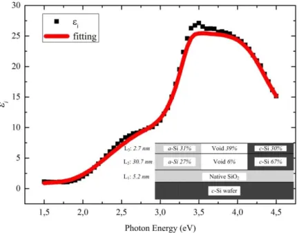
Figure 1.21 shows the measurement and the fitting results of a-Si:H deposited on c-Si wafer with native oxide by phase-modulated ellipsometry from 1.5 to 4.5 eV at an incident angle of 70°. The thickness of native oxide on c-Si substrate is fixed at 10 Å. As the oxidation is inevitable to occur on the surface of a-Si:H layer, in the model a top layer of SiO2/a-Si:H/void mixture was initially added, based on Bruggeman effective-medium
approximation [22]. The fitting result shows that the surface of a-Si:H is completely oxidized. Note that this measurement was carried out immediately after unloading the sample from the PECVD system at substrate temperature of 150°C, the thickness of grown
a-Si:H oxide layer is calculated around 3 Å. A series of measurement were carried out for
demonstrating that the continuous growth of oxide layer in ambient as a function of time, as listed in Table 1.1.
Figure 1.21 measurement and the fitting results of a-Si:H deposited on c-Si wafer with native oxide by a phase-modulated ellipsometry from 1.5 to 4.5 eV with incident angle of 70°.
32 1.2 THIN FILM DEPOSITION AND CHARACTERIZATION
Table 1.1 Fitting results of a-Si:H deposited on c-Si with native oxide after exposure to ambient air.
Time + 0 hour + 19 hours + 44 hours
Oxide of a-Si:H (Å) 3±1 10±2 14±2 a-Si:H (Å) 156±2 155±3 154±3 Eg (eV) 1.65±0.02 1.65±0.02 1.66±0.02 A 191±4 191±6 195±6 E0 (eV) 3.58±0.01 3.58±0.02 3.60±0.02 C 2.10±0.02 2.11±0.02 2.12±0.02 ε(∞) Fixed at 1.
1.3
L
ITHOGRAPHYThe word lithography is derived from ancient Greek “λίθος”, lithos in Latin letters, meaning “stone”, and “γράφειν”, graphein, meaning “to write”. In history, it was a method of printing texts from a stone or metal plate onto papers or other materials [23]. In modern semiconductor and integrated circuits (ICs) industry, micro-/nano- lithography technologies are applied to pattern the materials in small feature sizes down to submicron scale, accompanied with thin film deposition and wet/dry etching techniques.
In general, lithography techniques can be classified into two types [24]: (i) mask lithography, which use a pre-designed mask or template to transfer patterns on the substrates, including optical lithography, soft lithography, nanoimprint lithography and extreme ultraviolet (EUV) lithography; (ii) maskless lithography, which fabricates the patterns by in-situ writing without masks, including electron beam lithography, focused ion beam lithography, etc. In this thesis, optical lithography is used to pattern the substrate surface for the guided growth of in-plane SiNWs; electron beam lithography is used to define the electrode for measuring the resistivity of randomly grown in-plane SiNWs.
1.3.1 O
PTICAL LITHOGRAPHYOptical lithography defines patterns by exposing a light-sensitive resin (called photo-resist) to an ultraviolet (UV) light whose wavelengths range from 193 to 436 nm. The desired patterns are pre-designed on a transparent substrate (e.g. quartz or glass) with metallic opaque features (e.g. chrome) on it, through which the UV light is illuminated to the photo-resist which is spin-coated on the sample surface.
Take AZ5214-E [25] image reversal (IR) photo-resist used in this thesis for example: it is composed of a Novolak resin and Diazonaphthoquinone (DNQ) as photoactive compound (as shown in Figure 1.22), which is same as positive photo-resist. The UV exposure will release nitrogen from DNQ and transform it into a carboxylic acid, which is soluble in the aqueous alkaline solution based on NaOH, KOH, or TMAH (called developer). On the other hand, a baking step (called image reversal baking) after the UV exposure will produce a special crosslinking agent only in the exposed AZ5214-E, making this part of the photo-resist insoluble in developer as well as insensitive to the UV light, while the unexposed areas still behave like a normal unexposed positive photo-resist. After a flood exposure without photo-mask, only the crosslinked areas remain in the developer for positive photo-resist. Figure 1.23 illustrates the process of AZ5214-E as positive and image reversal photo-resist [26]. Also, it shows that the profile of positive photo-resist after development has a positive slope (75-85°), from which the name “positive” is derived. This is because during the exposure process, the UV light is attenuated when propagating through the photo-resist layer due to the absorption by the DNQ, called bulk effect, as shown in Figure 1.23 process 1. This type of positive tone is used as dry etching mask. On the other hand, the profile of IR photo-resist after development has a negative slope, also
34 1.3 LITHOGRAPHY
called undercut, which favours the lift-off process, as shown in Figure 1.24. A modified method for lift-off process is to introduce a mediated photo-resist layer (LOR for lift-off resist), which has different development rate with the AZ5214E so that the undercut can be formed for ensuring a discontinuous thin film deposition, as shown in Figure 1.25[27]. This method is also called bilayer lift-off.
Figure 1.22 Composition of AZ5214E photo-resist: (a) Novolak resin, (b) Diazonaphthoquinone (DNQ) [26].
Figure 1.23 Process of AZ 5214E as image reversal photo-resist: (1) exposure with photo-mask, (2) reversal bake, (3) flood exposure without mask, (4) development. After the first exposure (1), the image reversal resist would behave as a positive tone resist in the developer [26].