HAL Id: hal-00811652
https://hal-iogs.archives-ouvertes.fr/hal-00811652
Submitted on 10 Apr 2013
HAL is a multi-disciplinary open access
archive for the deposit and dissemination of
sci-entific research documents, whether they are
pub-lished or not. The documents may come from
teaching and research institutions in France or
L’archive ouverte pluridisciplinaire HAL, est
destinée au dépôt et à la diffusion de documents
scientifiques de niveau recherche, publiés ou non,
émanant des établissements d’enseignement et de
recherche français ou étrangers, des laboratoires
Multi-resonant absorption in ultra-thin silicon solar cells
with metallic nanowires
I. Massiot, Clément Colin, Christophe Sauvan, Philippe Lalanne, Pere Roca I
Cabarrocas, Jean-Luc Pelouard, Stéphane Collin
To cite this version:
I. Massiot, Clément Colin, Christophe Sauvan, Philippe Lalanne, Pere Roca I Cabarrocas, et al..
Multi-resonant absorption in ultra-thin silicon solar cells with metallic nanowires. Optics Express,
Optical Society of America - OSA Publishing, 2013, 21 (S3), pp.A372-A381. �10.1364/OE.21.00A372�.
�hal-00811652�
Multi-resonant absorption in ultra-thin
silicon solar cells with metallic nanowires
In`es Massiot,1Cl´ement Colin,1,2Christophe Sauvan,3Philippe
Lalanne,3Pere Roca i Cabarrocas,4Jean-Luc Pelouard,1and St´ephane Collin1,∗
1Laboratoire de Photonique et de Nanostructures (LPN-CNRS), Route de Nozay, 91460
Marcoussis, France
2Institut de Recherche et D´eveloppement sur l’Energie Photovolta¨ıque (IRDEP), UMR 7174
CNRS/EDF/Chimie-ParisTech, 6 quai Watier, 78401 Chatou, France
3Laboratoire Photonique, Num´erique et Nanosciences (LP2N), Universit´e Bordeaux
1/CNRS/Institut d'Optique, 33405 Talence Cedex, France
4Laboratoire de Physique des Interfaces et Couches Minces (LPICM-CNRS), Ecole
Polytechnique, 91128 Palaiseau Cedex, France
∗stephane.collin@lpn.cnrs.fr
Abstract: We propose a design to confine light absorption in flat and ultra-thin amorphous silicon solar cells with a one-dimensional silver grating embedded in the front window of the cell. We show numerically that multi-resonant light trapping is achieved in both TE and TM polarizations. Each resonance is analyzed in detail and modeled by Fabry-Perot reso-nances or guided modes via grating coupling. This approach is generalized to a complete amorphous silicon solar cell, with the additional degrees of freedom provided by the buffer layers. These results could guide the design of resonant structures for optimized ultra-thin solar cells.
© 2013 Optical Society of America
OCIS codes: (040.5350) Photovoltaic; (050.6624) Subwavelength structures; (250.5403) Plas-monics; (350.4238) Nanophotonics and photonic crystals; (040.6040) Silicon.
References and links
1. S. Benagli, D. Borrello, E. Vallat-Sauvain, J. Meier, U. Kroll, J. H ¨otzel, J. Bailat, J. Steinhauser, M. Marmelo, G. Monteduro, and L. Castens, “High-efficiency amorphous silicon devices on LPCVD-ZnO TCO prepared in industrial KAI-M R&D reactor,” in Proceedings of the 24th European Photovoltaic Solar Energy Conference (Hamburg, 2009), pp. 2293–2298.
2. P. Campbell and M. A. Green, “The limiting efficiency of silicon solar cells under concentrated light,” IEEE Trans. Electron. Dev. 33(2), 234–239 (1986).
3. D. L. Staebler and C. R. Wronski,“Optically induced conductivity changes in discharge-produced hydrogenated amorphous silicon,” J. Appl. Phys. 51(6), 3262–3268 (1980).
4. B. Rech and H. Wagner, “Potential of amorphous silicon for solar cells,” Appl. Phys. A 69, 155–167 (1999). 5. J. Krc, F. Smole, and M. Topic, “Potential of light trapping in microcrystalline silicon solar cells with textured
substrates,” Prog. Photovolt. Res. Appl. 11(7), 429-436 (2003).
6. C. Battaglia, K. S ¨oderstr¨om, J. Escarr´e, F-J. Haug, D. Domin´e, P. Cuony, M. Boccard, G. Bugnon, C. Denizot, M. Despeisse, A. Feltrin, and C. Ballif, “Efficient light management scheme for thin film silicon solar cells via transparent random nanostructures fabricated by nanoimprinting,” Appl. Phys. Lett. 96, 213504 (2010). 7. K. S ¨oderstr¨om, F. J. Haug, J. Escarre, O. Cubero, and C. Ballif, “Photocurrent increase in n-i-p thin film silicon
solar cells by guided mode excitation via grating coupler,” Appl. Phys. Lett. 96, 213508 (2010).
8. A. Abass, K. Q. Lee, A. Al`u, M. Burgelman, and B. Maes, “Dual-interface gratings for broadband absorption enhancement in thin-film solar cells,” Phys. Rev. B 85, 115449 (2012).
9. V. E. Ferry, M. A. Verschuuren, H. B. T. Li, E. Verhagen, R. J. Walters, R. E. I. Schropp, H. A. Atwater, and A. Polman, “Light trapping in ultrathin plasmonic solar cells,” Opt. Express 18, A237–A245 (2010).
10. V. E. Ferry, M. A. Verschuuren, C. van Lare, R. E. I. Schropp, H. A. Atwater, and A. Polman, “Optimized spatial correlations for broadband light trapping nanopatterns in high efficiency ultrathin film a-Si:H solar cells,” Nano Lett. 11(10), 4239–4245 (2011).
11. J. Zhu, C. M. Hsu, Z. Yu, S. Fan, and Y. Cui,“Nanodome solar cells with efficient light management and self-cleaning,” Nano Lett. 10, 1979–1984 (2010).
12. T. S ¨oderstr¨om, F.J. Haug, V. Terrazoni-Daudrix, and C. Ballif, “Optimization of amorphous silicon thin film solar cells for flexible photovoltaics,” J. Appl. Phys. 103, 114509 (2008).
13. M. Python, O. Madani, D. Domin´e, F. Meillaud, E. Vallat-Sauvain, and C. Ballif, “ Influence of the substrate geometrical parameters on microcrystalline silicon growth for thin-film solar cells,” Sol. Energ. Mater. and Sol. Cells 93, 1714–1720 (2009).
14. K. R. Catchpole and A. Polman, “Design principles for particle plasmon enhanced solar cells,” Appl. Phys. Lett. 93, 191113 (2008).
15. F. J. Beck, A. Polman, and K. R. Catchpole, “Tunable light trapping for solar cells using localized surface plasmons,” J. Appl. Phys. 105, 114310 (2009).
16. O. El Daif, L. Tong, B. Figeys, K. Van Nieuwenhuysen, A. Dmitriev, P. Van Dorpe, and F. Dross, “Front side plasmonic effect on thin silicon epitaxial solar cells,” Sol. Energ. Mater. and Sol. Cells 104, 58–63 (2012). 17. M. van Lare, F. Lenzmann, M. A. Verschuuren, and A. Polman, “Mode coupling by plasmonic surface scatterers
in thin-film silicon solar cells,” Appl. Phys. Lett. 101, 221110 (2012).
18. Y.-M. Chi, H.-L. Chen, Y.-S. Lai, H.-M. Chang, Y.-C. Liao, C.-C. Cheng, S.-H. Chen, S.-C. Tseng, and K.-T. Lin, “Optimizing surface plasmon resonance effects on finger electrodes to enhance the efficiency of silicon-based solar cells,” Energy Environ. Sci. 6, 935–942 (2013).
19. I. Massiot, C. Colin, N. P´er´e-Laperne, P. Roca i Cabarrocas, C. Sauvan, P. Lalanne, J-L. Pelouard, and S. Collin, “Nanopatterned front contact for broadband absorption in ultra-thin amorphous silicon solar cells,” Appl. Phys. Lett. 101, 163901 (2012).
20. H. A. Atwater and A. Polman, “Plasmonics for improved photovoltaic devices,“ Nat. Mater. 9(3), 205–213 (2010).
21. M. A. Green and S. Pillai, “Harnessing plasmonics for solar cells,“ Nat. Photon. 6, 130-132 (2012).
22. M. G. Moharam, E. B. Grann, D. A. Pommet, and T. K. Gaylord, “Formulation for stable and efficient imple-mentation of the rigorous coupled-wave analysis of binary gratings,” J. Opt. Soc. Am. A 12, 1068–1076 (1995). 23. P. Lalanne and G. M. Morris, “Highly improved convergence of the coupled-wave method for TM polarization,”
J. Opt. Soc. Am. A 13, 779–789 (1996).
24. A free version of the software “Reticolo” is available at http://www.lp2n.institutoptique.fr/Membres-Services/Responsables-d-equipe/LALANNE-Philippe.
25. P. Lalanne and M. P. Jurek, “Computation of the near-field pattern with the coupled-wave method for TM polar-ization,” J. Mod. Opt. 45, 1357–1374 (1998).
26. E. D. Palik, Handbook of Optical Constants of Solids (Academic, 1985), pp. 350-357.
27. F-J. Haug, T. S ¨oderstr¨om, O. Cubero, V. Terrazoni-Daudrix, and C. Ballif, “Influence of the ZnO buffer on the guided mode structure in Si/ZnO/Ag multilayers,” J. Appl. Phys. 106, 044502 (2009).
28. A. Cattoni, P. Ghenuche, A. M. Haghiri-Gosnet, D. Decanini, J. Chen, J. L. Pelouard, and S. Collin, ”λ3/1000
plasmonic nanocavities for biosensing fabricated by soft UV nanoimprint lithography,“ Nano Lett. 11, 3557– 3563 (2011).
1. Introduction
Thin film solar cells are a promising solution to reduce the overall cost of photovoltaic cells and increase production rates. In particular, remarkable progress has been made in amorphous sili-con (a-Si:H) solar cells technology leading to stable energy sili-conversion efficiencies of 10% with 250 nm thick a-Si:H [1]. Reducing further the absorber layer thickness towards ultra-thin (≤
100 nm) a-Si:H solar cells should improve the collection of current in the cell [2] as well as the stability against light-induced degradation [3, 4]. However, advanced light trapping strategies are needed to overcome the poor light absorption in thin semiconductor layers. Conventionally, random texturing of the interfaces [5, 6] is used to enhance the optical path length but is in-compatible with ultra-thin absorber layers. Numerous works have been done on light trapping through periodic nanopatterning of the back contact of the cell [7–11]. However, the growth of amorphous silicon on textured substrates leads to a reduction of the open-circuit voltage of the device because of the formation of cracks [12, 13]. Metallic nanostructures have also been in-tegrated at the front surface of the cell to scatter light in crystalline [14–16] or amorphous [17] silicon solar cells, or to realize partially transparent electrodes [18].
To achieve efficient a-Si:H photovoltaic devices, our objective is to design a light trapping scheme that would allow flat and very thin (≤ 100 nm) a-Si:H absorbers. In a previous work,
we have proposed a design based on an array of 1D silver wires embedded in an anti-reflection coating layer deposited on an ultra-thin amorphous silicon cell with a silver back mirror [19]. We proposed to use the nanopatterned metallic front layer as an alternative to the conventional transparent conductive oxide (TCO) front contact in order to reduce the absorption losses at short wavelengths. A theoretical short-circuit current density of 14.6 mA/cm2was numerically
demonstrated at normal incidence for a 90 nm-thick a-Si:H layer, with low polarization and angle dependencies. In this design, broadband absorption stems from multi-resonant light trap-ping. The absorption spectrum can be tuned by varying the different parameters of the structure. The origin of each absorption peak still needs to be carefully understood.
Here, we provide an in-depth analysis of the resonances involved in the multi-resonant light-trapping mechanism. We first consider a simple three-layer model based on a TCO/a-Si:H/Ag stack with a 1D silver grating embedded in the top TCO layer. Numerical simulations were performed using an exact RCWA method [22–24]. For TM polarization (magnetic field parallel to the wires), a semi-analytical treatment is used for the calculation of the fields and the absorp-tion [25]. The role of each key parameter of the structure (TCO layer thickness, a-Si:H thickness and grating period) in the absorption is analyzed. We apply this multi-resonant approach to the design of a complete solar cell with two buffer layers giving additional degrees of freedom to optimize further the absorption in the cell. This work can be generalized to other thin-film materials in order to conceive ultra-thin solar cells with resonant light trapping designs.
2. Design of 1D plasmonic nanostructures for ultra-thin a-Si:H solar cells
We consider a simplified three-layer structure, see Fig. 1(a). Light confinement is achieved with a 1D metallic grating (width w, pitch p, metal thickness hm) deposited on an amorphous
silicon absorber layer (thickness hs) and a metallic mirror as a back contact. In amorphous
silicon solar cells, the TCO layer is conventionally made of indium tin oxide (ITO) or aluminum doped zinc oxide (ZnO:Al). In the following, we considered ZnO:Al only. The top ZnO:Al layer (thickness h1) is used both as an anti-reflection coating layer and as a front contact. We define
a structure based on an a-Si:H absorber layer with a thickness hs= 90 nm and a patterned silver
layer (hm= 20 nm) embedded in a TCO layer (h1= 60 nm). The corresponding metallic grating
consists of silver wires with w= 80 nm and p= 200 nm. This structure will be used as a reference for the analysis developed in the following.
The refractive index of silver is taken from Ref. [26]. The refractive indices of a-Si:H (nS)
and ZnO:Al (n1) have been measured by ellipsometry.
The calculated optical response of the reference structure at normal incidence is shown in Fig. 1(b). Broadband absorption is achieved for both TE and TM light polarizations. Remark-ably, despite the strong anisotropy of the structure, high performance is achieved for both po-larizations. This is due to the presence of six resonances (three for each polarization) that are judiciously combined by the design. The main absorption peaks identified in this structure are
λAE=476 nm,λBE=631 nm,λCE=687 nm for TE andλAM=430-550 nm,λBM=537 nm,λCM=649
nm for TM light polarizations. In the following section, we analyze the physical origin of the resonances.
For the sake of simplicity, only the total absorption spectrum is analyzed in section 3. Note that it enables to show resonances that would not contribute to the generation of current because they are below the energy bandgap. The absorption fraction in each layer of the stack is detailed in section 4 for a complete amorphous silicon solar cell. It shows that the same peak positions are obtained for the absorption in each part of the cell.
Fig. 1. (a) Schematic of the simplified structure made of a ZnO:Al/a-Si:H/Ag stack. A 1D silver grating (width w, pitch p, metal thickness hm) is deposited on the a-Si:H layer
(thickness hs) and embedded in a ZnO:Al anti-reflection coating layer (thickness h1). (b)
Spectra of the numerically computed total absorption of the reference structure under TM (orange) and TE (green) polarized light at normal incidence. The parameters of the metallic grating are p=200 nm, w=80 nm and hm=20 nm. The total absorption spectrum of a planar
ZnO:Al (50 nm)/a-Si:H (90 nm)/Ag structure is shown with the black dashed curve for the sake of comparison.
3. Analysis of the multi-resonant absorption mechanism
In this section, we provide a physical analysis of the multi-resonant mechanism. To do so, we numerically study the evolution of the total absorption spectrum as a function of three important design parameters (ZnO:Al and a-Si:H thicknesses and the grating period) and we propose a simple analytical model to fit the numerical results.
3.1. Absorption resonances in the top ZnO:Al layer: resonances AE& AM
Let us consider the absorption peaks observed at short wavelengths (resonances AEand AM).
We first study the evolution of the absorption spectrum when the thickness h1of the ZnO:Al
layer varies from 20 to 170 nm. For h1= 20 nm, the ZnO:Al exactly fills the grooves. Figure 2
displays the total absorption spectrum in the structure as a function of the ZnO:Al layer thick-ness h1. At long wavelengths (λ > 600 nm), absorption bands independent of h1are attributed
to resonances BE, CE, BMand CMas shown with orange dashed lines in Figs. 2(b) and 2(c). At
shorter wavelengths (λ< 600 nm), the TE and TM absorption diagrams exhibit two absorption
bands (black dashed curves) that strongly depend on the ZnO:Al layer thickness.
We consider the top ZnO:Al layer as an asymmetric Fabry-Perot resonator withφ1andφ2the
phase shifts induced by reflection at the ZnO:Al/Air and ZnO:Al/a-Si:H interfaces as depicted in Fig. 2(a). The influence of the metallic grating is neglected as a first approximation. In the Fabry-Perot model, the resonance condition in such a cavity can be written as
Fig. 2. Study of the short wavelengths resonances (AE) (TE) and (AM) (TM). (a) Sketch
of the asymmetric Fabry-Perot resonator model used to fit the numerical calculations. The influence of the metallic grating is neglected.φ1andφ2 are the phase shifts induced by
reflection at the ZnO:Al/Air and ZnO:Al/a-Si:H interfaces. (b, c) Total light absorption spectrum in the simplified structure depicted in Fig. 1 as a function of the wavelength and the ZnO:Al layer thickness h1. Excitation at normal incidence light in (b) TE and (c)
TM polarizations. The position of the absorption bands with low dependence on h1 can
be attributed to resonances BE, CE, BMand CMas shown with orange dashed lines. The
resonance position h1= f (λ) given by the Fabry-Perot model (Eq.( 1)) is shown with black
dashed curves for q= 0, 1.
h1= λ
2n1
(q − ϕ
2π) (1)
with n1the refractive index of the ZnO:Al layer and q an integer. The total phase shiftϕ is
defined byϕ =φ1+φ2. From numerical calculations, we find thatφ1andφ2vary slowly in
the vicinity of the resonances. Thus, we use a constant value forϕ in the Fabry-Perot model (ϕ∼ -1.89 rad). The corresponding curves h1= f (λ) obtained from Eq. (1) with q = 0, 1 are
shown in Figs. 2(b) and 2(c) with black dashed curves. The latter remarkably well predict the absorption bands of the structure. The resonances AEand AMcan thereby be attributed to the
lowest order mode (q= 0) of the Fabry-Perot resonances in the cavity Air/ZnO:Al/a-Si:H. Note
that the Fabry-Perot resonance occurs in the ZnO:Al layer but leads to absorption in the active a-Si:H layer.
At short wavelengths (450-500 nm), the metallic grating has a minor effect on the optical response of the device in TM polarization, giving rise to a splitting of the resonance AM. As
shown in Fig. 2, the error in the spectral position of the peaks with respect to the Fabry-Perot model increases with the wavelength.
3.2. Absorption resonances in the a-Si:H layer: resonances BE& BM
The nature of resonances BEand BMis now investigated. Figure 3 displays the evolution of the
predicted total absorption under (b) TE and (c) TM polarizations as a function of the absorber layer thickness hs. We first note that hshas only a minor influence on the absorption bands
dis-cussed in section 3.1, in agreement with the Fabry-Perot interpretation of Air/ZnO:Al/a-Si:H resonances. On the contrary, according to Figs. 3(b) and 3(c), the absorption peaks correspond-ing to BE and BM have a spectral position and an intensity that both strongly depend on hs.
We thereby consider an asymmetric Fabry-Perot resonator (see Fig. 3(a)) and we can adapt the resonance condition of Eq. (1) with h1= hs and n1= ns. As in the previous subsection, the
Fig. 3. Study of the resonances (BE) (TE) and (BM) (TM).(a) Sketch of the asymmetric
Fabry-Perot resonator model used to fit the numerical calculations. The influence of the metallic grating is neglected.φ1andφ2 are the phase shifts induced by reflection at the
a-Si:H/ZnO:Al and a-Si:H/Ag interfaces. (b, c) Total light absorption spectrum in the sim-plified structure depicted in Fig. 1 as a function of the wavelength and the absorber layer thickness hs. Excitation at normal incidence light in (b) TE and (c) TM polarizations. The
resonance position hs= f (λ) given by the Fabry-Perot model (Eq.( 1)) with h1= hsand
n1= ns, is shown in black dashed lines for q= 0, 1, 2, 3. (d,e) Electric field intensity
maps for a 1D silver grating with w= 80 nm, p= 200 nm, hm= 20 nm for an excitation at
(d)λBE= 631 nm under TE polarized light and (e)λBM= 649 nm under TM polarized light.
The corresponding curves hs= f (λ) are plotted in Figs. 3(b) and 3(c) with black dashed lines
for different values of the integer q. For both BEand BM resonances, the Fabry-Perot model
is in qualitative agreement with the RCWA calculations. Both absorption peaks can thereby be attributed to Fabry-Perot resonances within the a-Si:H layer (mode with q= 0).
Figures 3(d) and 3(e) display the spatial distribution of the electric field intensity between the silver strips when the structure is excited atλ=631 nm (TE, resonance BE) andλ=649 nm (TM,
resonance BM). In TE polarization, the field maximum is located within the a-Si:H layer with a
low field intensity in the metal. In the case of the resonance BE, the effect of the metallic grating
is thereby negligible. In TM polarization, there is a field exaltation on the edges of the silver. Consistently, there is a much larger difference betweenλBM and the wavelength predicted by
the Fabry-Perot model.
3.3. Absorption resonances induced by guided modes: resonances CE& CM
The last resonance contributing to the absorption in the a-Si:H layer in TE polarization, called CE, involves a different mechanism. We have investigated the influence of the angle of
inci-dence θ (plane of incidence perpendicular to the wires) and the grating period p on the ab-sorption spectrum of the structure. The results are shown in Figs. 4(a) and 4(b). The abab-sorption peak corresponding to the resonance CE is the only one exhibiting a dispersive character as
Fig. 4. Study of the long wavelength (CE) resonance for TE polarization. (a) Total light
absorption spectrum as a function of the wavelength and the angle of incidence (plane of incidence perpendicular to the wires). (b) Total light absorption spectrum as a function of the wavelength and the grating period at normal incidence. The absorption bands attributed to resonances AEand BE are shown in orange dashed lines in Figs. 4 (a) and (b). (c)
Elec-tric field intensity map for an excitation atλCE= 687 nm for a TE polarization at normal incidence.
excitation at wavelengthλCE in TE polarization. The grating efficiently traps light because of
the excitation of a waveguide mode supported by the a-Si:H layer as shown in previous studies on a-Si:H solar cells with periodic patterns [7, 9]. Indeed, the grating supplies an extra momen-tum so that the coupling of the incident light with a diffracted mode of order m could satisfy the conservation of the in-plane momentum and excite an eigenmode of the TCO/a-Si:H/Ag waveguide: 2π λCE Re(ne f f) = | 2π λCE sinθ+ m2π p | (2)
with m a relative integer and ne f f the effective index of the waveguide mode. Equation (2) is
valid provided that one neglects the effective index change induced by the silver grating. We consider the mode resulting from the coupling to the diffracted order m= -1 and guided in the ZnO:Al/a-Si:H/Ag waveguide under TE polarization. Using Eq. (2), we have plotted the
θ= f (λCE) curve for the structure with p=200 nm in Fig. 4(a) (white dashed line). It agrees well
with the shift ofλCE predicted by the RCWA calculations asθincreases. We have also plotted
the curve p= f (λCE) given by Eq. (2) at normal incidence for m= -1. The result displayed in
Fig. 4(b) (black dashed curve) fits well with the spectral position predicted by the numerical calculations. An additional peak resulting from the coupling of the guided mode to a higher order diffracted mode (m= -2) appears for a grating period p over 425 nm as shown in Fig. 4(b) (black solid line).
The attribution of the resonance CEto an eigenmode of the ZnO:Al/a-Si:H/Ag waveguide
also explains the evolution of the total absorption spectrum when the a-Si:H layer thickness
hs varies. Indeed, the effective index of the guided mode increases with the thickness of the
guiding layer, leading thereby to a shift ofλCE towards higher wavelengths. This is in good
agreement with the spectral shift observed in Fig. 3(b).
Finally, it is worth noticing that the absorption peak atλ= 770 nm for TM polarization, la-belled CM, can also be attributed to a guided mode supported by the a-Si:H layer. This resonance
involves surface plasmons propagating at the a-Si:H/Ag interface thereby leading to parasitic absorption in the metallic mirror. As shown in Fig. 1, it leads to an absorption peak at an en-ergy below the electronic bandgap of the absorber material. In the following, we show that this resonance can be shifted by the addition of a ZnO:Al buffer layer between the absorber layer and the back mirror and hence contribute to the generation of photocurrent in the structure (see subsection 4.2).
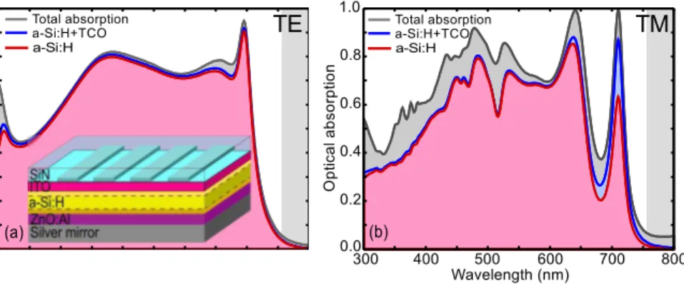
Fig. 5. Numerically computed optical absorption in each material of an ultra-thin a-Si:H solar cell for an excitation under TE (a, left) and TM (b, right) polarizations at normal inci-dence (red curve: absorption only in a-Si:H; blue curve: absorption in a-Si:H and the ITO and ZnO:Al spacing layers; grey curve: total absorption). The bandgap of amorphous sili-con is shown in grey. Inset of Fig. (a): Sketch of the structure investigated: solar cell made of a Si3N4(Ag)/ITO/a-Si:H/ZnO:Al/Ag stack with a 90 nm-thick p-i-n a-Si:H absorber
layer. A 1D silver grating (thickness=20 nm, width=80 nm and period=200 nm) is embed-ded in the front Si3N4layer. Other geometrical parameters are hSi3N4=60 nm, hITO=10 nm,
hZnO:Al=15 nm.
4. Application to ultra-thin amorphous silicon solar cells
4.1. Description of the complete cell
A complete photovoltaic cell is described in the inset of Fig. 5(a). The a-Si:H active layer is composed of a p-i-n junction, the influence of the doping on the refractive index of the material is neglected in this analysis. Two additional spacing layers are inserted above (ITO) and below (ZnO:Al) the a-Si:H layer to prevent metal diffusion in the absorbing layer. As shown in section 3 for the simplified structure, the use of the 1D silver grating leads to a multi-resonant and broadband absorption spectrum. The top ZnO:Al layer is replaced by a non-absorbing material (silicon nitride, Si3N4). The top contact is then formed by the ITO spacing layer and the metallic
grating, resulting in a reduction of optical absorption in the top layers of the structure at short wavelengths.
4.2. Design rules and influence of the ZnO:Al buffer layer
In section 3, we have identified the role of each geometrical parameter of the structure in the absorption resonances. This analysis provides guidelines for the design of the complete solar cell depicted in the inset of Fig. 5(a), as summarized in Table 1. The top anti-reflection layer (Si3N4) thickness is set at 60 nm for a resonance at 450-500 nm. The thickness of a-Si:H layer
is 90 nm and contributes to absorption enhancement in the 600-650 nm wavelength range. With a period of 200 nm, the grating leads to the excitation of guided modes in both TE and TM polarizations at a wavelength close to 700 nm.
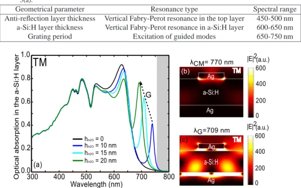
We now investigate the influence of the two additional spacing layers. The influence of the ZnO:Al layer thickness on the absorption in the a-Si:H layer is displayed in Fig. 6(a) for TM polarization. In Ref. [27], Haug et al. reported that the ZnO:Al buffer layer between the a-Si:H absorber layer and the back silver mirror could have a beneficial effect on the absorption in the active layer. Let us compare the resonance labelled CM in Fig. 1 to the absorption peak, at λG=709 nm in Fig. 6(a). Figures 6(b) and 6(c) display the electric field intensity maps
Table 1. Influence of the geometrical parameters of the structure shown in the inset of Fig. 5(a).
Geometrical parameter Resonance type Spectral range Anti-reflection layer thickness Vertical Fabry-Perot resonance in the top layer 450-500 nm
a-Si:H layer thickness Vertical Fabry-Perot resonance in a-Si:H layer 600-650 nm Grating period Excitation of guided modes 650-750 nm
Fig. 6. (a) Evolution of the absorption in the a-Si:H layer for the complete cell as a function of the ZnO:Al layer thickness hAZO for a TM polarized light at normal incidence. (b, c)
Electric field intensity maps for an excitation atλCM= 770 nm (simplified structure)(b) and λG= 709 nm (complete cell)(c) at normal incidence for a TM polarization.
absorber layer. This agrees with the attribution of these peaks to a low energy guided mode ob-served under TM polarization. Besides, adding a low index buffer layer leads to a decrease of the effective index of the guided mode. This is consistent with the shift towards shorter wave-lengths observed in Fig. 6(a) when hZnO:Alincreases. The thickness of the buffer layer allows us
to tune the spectral position of the peak corresponding to the guided mode G. However, increas-ing hZnO:Al induces a decrease of the absorption intensity atλ= 635 nm because of increased
absorption losses in the buffer layer, as evidenced in Fig. 6.
Therefore, the buffer ZnO:Al layer thickness is fixed to the value of 15 nm in order to achieve an optimal broadband absorption spectrum favored by a lower spectral position of the peak while limiting the fraction of incident photons absorbed in the buffer layer. Finally, the thickness of the ITO spacing layer between the metallic grating and the a-Si:H layer is chosen to be as low as possible (hIT O=10 nm) to avoid parasitic losses in this layer.
The optical response of the resulting structure is shown in Figs. 5(a) and 5(b). The multi-resonant absorption spectra are very similar to those obtained for the simplified reference struc-ture described in section 2. The absorption peaks at short wavelengths (λ ≤ 700 nm) are due
to Fabry-Perot resonances in the Si3N4layer and a-Si:H layers. At long wavelengths, close to
the a-Si:H bandgap, sharper peaks corresponding to resonances CE (TE) and CM (TM) of the
4.3. Predicted performances of the cell
In section 3, the analysis of the multi-resonant mechanism was performed by considering the total absorption in the whole structure. In Figs. 5(a) and 5(b), we show the absorption fractions in each material constituting the solar cell for TE and TM polarizations. For the absorption peaks at λ= 636 nm and 709 nm in TM polarization, perfect absorption is achieved in the structure: the critical coupling condition is achieved for these two resonances [28]. However, as shown in Fig. 5(b), there are non negligible parasitic absorption losses in the metallic grating in TM polarization.
We used the absorption spectrum in the a-Si:H active layer (red curve) to calculate the the-oretical short-circuit current density of the cell, assuming that all photogenerated carriers are collected [19]. A JSC of 14.6 mA/cm2 is predicted for a cell with a 90 nm-thick a-Si:H
ab-sorber layer. In order to evaluate the global performances of the cell, we used state-of-the-art values [7] for the open-circuit voltage (VOC=0.88 V) and fill factor (FF= 0.7) leading to a
the-oretical conversion efficiency of 9%.
5. Conclusion
In summary, we have studied the multi-resonant absorption mechanism achieved in ultra-thin a-Si:H solar cells with a patterned metallic front contact. The three resonances observed for TE and TM polarizations are analyzed by simple models, and attributed to Fabry-Perot resonances in the ZnO:Al and a-Si:H layers, and the excitation of guided modes via grating coupling. This detailed analysis is a powerful tool to optimize a design without exploring the whole param-eter space. We have generalized this approach to a complete a-Si:H solar cell. An additional ZnO:Al buffer layer is used to tune the absorption spectrum and reduce the parasitic losses in the metallic parts. This multi-resonant approach is broadly applicable to other thin-film solar cell materials such as GaAs or CIGS. This work could guide the optical design of solar cells with multi-resonant light trapping schemes.
Acknowledgments
The authors would like to thank A. Cattoni and J. F. Guillemoles for fruitful discussions. This work was partially supported by the ANR projects ULTRACIS and NATHISOL.