HAL Id: hal-00339858
https://hal.archives-ouvertes.fr/hal-00339858
Preprint submitted on 19 Nov 2008
HAL is a multi-disciplinary open access
archive for the deposit and dissemination of
sci-entific research documents, whether they are
pub-lished or not. The documents may come from
teaching and research institutions in France or
abroad, or from public or private research centers.
L’archive ouverte pluridisciplinaire HAL, est
destinée au dépôt et à la diffusion de documents
scientifiques de niveau recherche, publiés ou non,
émanant des établissements d’enseignement et de
recherche français ou étrangers, des laboratoires
publics ou privés.
Successful Attack on an FPGA-based Automatically
Placed and Routed WDDL+ Crypto Processor.
Laurent Sauvage, Sylvain Guilley, Jean-Luc Danger, Yves Mathieu, Maxime
Nassar
To cite this version:
Laurent Sauvage, Sylvain Guilley, Jean-Luc Danger, Yves Mathieu, Maxime Nassar. Successful
At-tack on an FPGA-based Automatically Placed and Routed WDDL+ Crypto Processor.. 2008.
�hal-00339858�
Successful Attack on an FPGA-based Automatically Placed and Routed WDDL+
Crypto Processor.
Laurent SAUVAGE, Sylvain GUILLEY, Jean-Luc DANGER, Yves MATHIEU and Maxime NASSAR
Institut TELECOM, TELECOM ParisTech
CNRS LTCI (UMR 5141)
Dpartement COMELEC, 46 rue Barrault
75 634 PARIS Cedex 13, FRANCE
Email: < laurent.sauvage@telecom-paristech.fr >
Abstract
In this paper, we report the first successful attack on a DES crypto co-processor protected by the “Positive” Wave Dynamic Differential Logic (WDDL+) and embedded in a Field Programmable Gates Array (FPGA). This attack is unambiguous as the full key is retrieved. We experimentally show that this countermeasure resists to Differential Power Analysis (DPA), but can be broken by a totally non-invasive Electro-Magnetic Analysis (EMA) method. The method re-lies on two stages, the first being a localisation phase by means of cartography, and the second being the EMA at-tack on the most relevant area.
Keywords: Side-Channel Analysis (SCA), Differential
Power Analysis (DPA), Differential Electro-magnetic Anal-ysis (DEMA), Wave Dynamic Differential Logic (WDDL), Field Programmable Gates Array (FPGA).
1
Introduction
To defeat Side-Channel Analysis (SCAs), many solu-tions have been proposed since the first attack published 10 years ago [9].
The Dual-rail with Precharge Logic (DPL) is a counter-measures family which try to make the power consumption independent of the manipulated data. In this family, we find the Wave Dynamic Differential Logic (WDDL) coined by Kris Tiri [16]. The major advantage of this latter is the use of a standard cell flow, which facilitates the synthesis process. Moreover this enables implementation on Com-ponents Off The Shelf (COTS) such as FPGAs. Although WDDL presents a flaw [14] like the ”early evaluation” bias, by now nobody exploits it to lead a complete successful at-tack. Whereas, Sylvain Guilley and al. stepped into the
breach in [5]: with the seminal Differential Power Analy-sis (DPA), they break one SBox of a FPGA-based WDDL+ DES module embedded on a “Parallax Stratix 672 Smart-Pack Board”. This disproves statement that DPA on com-mercial FPGA development board is difficult [13].
In this paper, we are going one step further by announc-ing the first successful attack on a FPGA-based WDDL+ DES crypto co-processor. This attack is fully non invasive: no board modifications are required as it is performed with the Differential Electro-Magnetic Analysis (DEMA). Far-field DEMA attacks have already been reported in [8, 7]. The strength of our new attack relies on a method whose first phase is a 2D cartography allowing the attacker to find the precise location of the targeted crypto module activ-ity [12]. By carefully positioning the antenna, the number of measurements to disclose (MTD) the key of a non-protected crypto module could be hundred times smaller compared to DPA.
The rest of the paper is organized as follows: Section 2 recall some informations about the concepts applied in our experiments. The target of our attack s described in Sec. 3. Section 4 presents our results, and finally, conclusions and perspectives are given in the Sec. 5.
2
Related Works
2.1
WDDL
To achieve a constant power consumption, the differen-tial DPL logic styles are used in order to ”hide” the secret leakage. The logic properties are both spatial (differen-tial logic) and temporal (two phases). A differen(differen-tial logic is such that every variable x is shared in two signals: the
”True” xT and the ”false” xF, involving a ”Dual Rail”
logic networks, True and False, receiving respectively the True and the False signals. The DPL temporal property consists in splitting the calculation in two phases: precharge and evaluation. During the precharge phase the signals are forced in a state such that the number of transitions is con-stant when switching from the precharge to the evaluation phase, and vice versa. As the power consumption is di-rectly related to the number of transitions in CMOS tech-nology, the activity is constant whatever the variables val-ues. For instance in WDDL the precharge phase is such that all the signals are reset to the value 0. This value is prop-agated along the logic cones as the True and False logic networks are composed with positive functions only. When switching a variable x enters the evaluation phase, either
xT or xF goes from 0 to 1 but never both. DPL needs a
perfect balance between the True and False networks prop-agation time otherwise bias like early evaluation makes at-tacks possible as explained in [15]. Consequently the design flow needs special at the synthesis (front-end) and place and route (back-end) stages. The back-end operations are not so easy when targeting FPGA [1, 2] where interconnects structure is imposed by the vendor. . In ASICs, back-end technique’s like fat wire [17] and back-end duplication [3] permits the generate of well balanced designs. The bias like early evaluation is difficult to mitigate. Patrick Schaumont propose a solution for FPGAs in [18]. It consists in dupli-cating the WDDL such a way that the True and False Net-works are inverted between the two WDDL instances. This is however rather costly as the complexity is at least mul-tiplied by 4 w.r.t. a non protected design. In ASICs some secure libraries have been developed. The one developed in [4] relies on synchronization between signals ans offers a great level of protection. In this paper we target a WDDL implementation which has no specific effort of Placing and Routing but which remains unattacked until now.
Another bias of WDDL comes from the glitches genera-tion if WDDL is not implemented in a proper way [5]. The use of positive functions solves this problem and delivers what we call “Positive” WDDL (WDDL+). We evaluate in this paper the robustness of this latter.
2.2
ElectroMagnetic Cartography
The new attack takes advantage of a two-step method, whose first one consists in spotting the best location to at-tack. One of the first EM cartography of an integrated cir-cuit (IC) to be reported is that of J.-J. Quisquater and D. Samyde on an 8-bit smart card processor [10]. The princi-ple is to acquire temporal traces for every point of a 2D grid covering all or only a part of the targeted chip. This grid corresponds to the set of positions of the antenna placed by means of a X-Y motor driven table. Then, a post processing has to be applied on the temporal traces to build the final
map.
In the temporal domain, the post processing to attack a cryptoprocessor can be the computation of the difference between the maximum amplitude of the EM field and the mean amplitude of differential traces. In the frequency do-main, the Discrete Fourier Transform (DFT) of each trace (i.e. each point) permits the detection of a specific fre-quency intrinsic to the attacked module.
The same exercise on other devices (for instance FPGAs) has not been reproduced, and therefore, the EM exploration of deep-sub micron device remains an open topic of re-search, especially in the field of trusted computing. The second step is to attack the selected location(s) by DEMA.
3
The FPGA-based crypto SoC
Several experiments to evaluate the security of an imple-mentation relies on the design of only a part of a crypto-graphic algorithm. With no special care, when performing analysis, emerging correlations could be du to this restric-tion on the design, whereas we are looking for correlarestric-tions du to the inside computations. For example, considering the obvious test of a single Substitution Boxes (SBoxes) of DES or AES. If the output of the SBoxes is provided outside of the chip for computation checking, correlations comes from the power consumption (or the EM field) of the I/O slots, not from the power consumption of the SBoxes logic elements.
To prevent from such problem and attack a real-life ap-plication, we design a complete System on Chip (Soc) including a master processor for I/O communication and crypto co-processors for encryption with standard algo-rithms such as DES, 3DES, AES. This way, total control on I/O operations is done, and none occur during computa-tions.
The Soc includes unprotected modules which serve as reference to evaluate security of protected ones. We can see on the Fig. 1 the floorplan of the Soc, with 2 regular DES modules (references) on the top left and bottom left corners, and the WDDL+ module and the right.
The Soc is programmed in an EP1S25 “Stratix” Al-tera FPGA (130 nanometers technology), embedded on a “SHIX2.0”, an 8-layer PCB professional board.
4
Experimental Results
As background material, we used antennas of the “HZ-15 Probe Set” [6] from “Rohde and Schwarz” [11], and two pre-amplifiers for an overall gain of 60 dB in the frequency range from 100 kHz to 3 GHz. The output signal of the pre-amplifiers is digitized by an 54855 Infiniium Agilent oscilloscope whose bandwidth is 6 GHz and maximal
sam-DES2
DES1
DES in WDDL
Figure 1. Floorplan of the system-on-chip programmed in a Stratix.
ple rate is 40 GSa/s. The antenna is mounted on a 2D mo-torized table and moved over the FPGA through an area of
2.08cm× 2.00 cm. The resolution is of 50 points on X
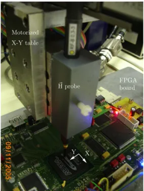
and on Y. In others words, the mechanical step is equal to 40 µm. Fig. 2 is a photographic of the experimental setup, with the antenna over the most leaking point.
4.1
Spotting by Cartography
The acquisition needs no averaging or synchronization as it could be the case for a post processing exploiting the temporal characteristics. Indeed, averaging is powerful to reduce the noise and to discern pattern in a temporal traces, but as the method focus on a specific frequency, contribu-tion of the noise on this latter is minimum because it is spread over the entire frequency range. As a consequence, this slightly reduces the number of message to be inter-cepted. To prove our ability to distinguish precise areas of the FPGA, we have build the map for a frequency of 100 MHz (fourth harmonic of the FPGA clock frequency of 20 MHz). The results is depicted by the Fig. 3 (left). The dashed rectangle is a landmark which delimits the ASIC of the FPGA. On the right, the scale gives the voltage dynamic range at the output of the antenna (proportional to the EM field). The highlighted area on the left bottom of the picture corresponds to the bound wires carrying the 20 MHz master clock.
Now, to locate the WDDL+ co-processor, we have to
Y X Motorized FPGA board ~ H probe X-Y table
Figure 2. The antenna over the “SHIX2.0” board and the FPGA.
guess its frequency signature. As explained is Sec. 2.1, WDDL runs in 2 phases: precharge and evaluation. In our implementation, they occur on the rising edge of the SoC clock, which frequency is 8.333 MHz. Indeed, internal fre-quency of the WDDL+ DES co-processor can be viewed as being equal to half of this of the SoC clock, and then equal to 4.166 MHz. The map for this latter is given by the Fig. 3 (right).
Four area are standing out: two in the top and two in the right of the figure. The Tab. 1 gives the coordinates and the amplitude of their maximum.
Table 1. Coordinates and Amplitudes of the Maximums. Area X [cm] Y [cm] Amplitude [nV] 1 0.374 1.560 0.806 2 0.416 1.000 0.792 3 -0.041 1.680 0.762 4 0.832 1.040 0.685
0 20 40 60 80 100 120 V [nV] -1 -0.5 0 0.5 1 X [cm] 0 0.5 1 1.5 2 Y [cm] 0 0.2 0.4 0.6 0.8 1 1.2 V [nV] -1 -0.5 0 0.5 1 X [cm] 0 0.5 1 1.5 2 Y [cm]
Most leaking area
Figure 3. EM field at 100 MHz (left) and 4.333 MHz (right). -40 -30 -20 -10 0 10 20 30 40 50 0 0.2 0.4 0.6 0.8 1 V [nV] t [µs]
Figure 4. EM field at X=0.416 cm and Y=1 cm.
4.2
EMA Attack
For all the relevant areas, a new acquisition has been performed. The acquired traces are the mean of 256 real traces grabbed by the oscilloscope with performs the aver-aging and is triggered by an external signal to get coherent traces. The attack on the R register has been lead after the first round of DES. On the rest of the paper, we will focus on this which gives the best results, the number 2, marked “Most leaking area”. A 256 times averaged temporal trace of the EM field at this point is depicted by the Fig. 4. We can observe that the EM field is negative for the precharge, positive for the evaluation. This could be explained by the current inversion of the CMOS capacitors. At the beginning of the precharge phase, the CMOS gates of WDDL go from
1to 0 , whereas this is the other way round when switching
from the precharge phase to the evaluation phase.
Tab. 2 recalls the minimum number of MTD needed for Power Analysis.
For the regular DES module, the best results are obtained by guessing the hamming distance of 4 bits of the R regis-ter (coming from the output of each Sbox). For WDDL+,
-40 -30 -20 -10 0 10 20 30 40 0 0.2 0.4 0.6 0.8 1 Covariance factor [%] t [µs] SBox1 -40 -30 -20 -10 0 10 20 30 40 0 0.2 0.4 0.6 0.8 1 Covariance factor [%] t [µs] SBox2 -40 -30 -20 -10 0 10 20 30 40 0 0.2 0.4 0.6 0.8 1 Covariance factor [%] t [µs] SBox3 -40 -30 -20 -10 0 10 20 30 40 0 0.2 0.4 0.6 0.8 1 Covariance factor [%] t [µs] SBox4 -40 -30 -20 -10 0 10 20 30 40 0 0.2 0.4 0.6 0.8 1 Covariance factor [%] t [µs] SBox5 -40 -30 -20 -10 0 10 20 30 40 0 0.2 0.4 0.6 0.8 1 Covariance factor [%] t [µs] SBox6 -40 -30 -20 -10 0 10 20 30 40 0 0.2 0.4 0.6 0.8 1 Covariance factor [%] t [µs] SBox7 -40 -30 -20 -10 0 10 20 30 40 0 0.2 0.4 0.6 0.8 1 Covariance factor [%] t [µs] SBox8
Figure 5. Covariance factors obtained for the correct key hypothesis when attacking the first round of the WDDL+ DES module.
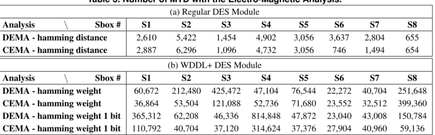
because of the precharge, the best results are obtained by guessing the hamming weight of these 4 bits. In this last case, only one Sbox is broken, which experimentally prove that WDDL+ is well suited to protect from Power Analysis. Results for the Electro-Magnetic Analysis are reported in the Tab. 3.
Its superiority to the C/DPA is well illustrated as the number of MTD for the regular DES module is hundred times less. For WDDL+, it enables to retrieve the secret key in less than 399,360 messages.
In dual rail logic, close bits are attended to balance their power consumption. Indeed, guessing 4 bits could be more efficiency that only one. The bottom of the Tab. 3 shows it isn’t really the case.
Finally, Fig. 5 presents for each Sbox the differential traces obtained after the “CEMA - hamming weight” on the protected module.
Another stunning effect is that correlation occurs for cer-tain Sboxes on the precharge phase.
5
Conclusion and Perspectives
We have reported the first successful attack on an FPGA-based automatically placed and routed WDDL+ DES crypto processor. WDDL+ is well suited against DPA, but fails against the new EMA technique presented in this paper.
Open question is the impact of the constrained place and route on the security. Some answers can be found in [1, 18], but the ultimate one would be given further with a clone of the attack presented here on well placed and routed WDDL+ module.
Table 2. Number of MTD with the Power Analysis.
(a) Regular DES Module
Analysis \ Sbox # S1 S2 S3 S4 S5 S6 S7 S8
DPA - hamming distance 632,128 196,160 510,912 670,272 461,824 710,592 491,392 144,448
CPA - hamming distance 478,720 197,056 464,128 614,720 418,944 709,056 348,288 134,080 (b) WDDL+ DES Module
Analysis \ Sbox # S1 S2 S3 S4 S5 S6 S7 S8
DPA - hamming weight — — — — 7,919,552 — — —
CPA - hamming weight — — — — — — — —
Table 3. Number of MTD with the Electro-Magnetic Analysis.
(a) Regular DES Module
Analysis \ Sbox # S1 S2 S3 S4 S5 S6 S7 S8
DEMA - hamming distance 2,610 5,422 1,454 4,902 3,056 3,637 2,804 655
CEMA - hamming distance 2,887 6,296 1,096 4,732 3,056 746 1,494 654 (b) WDDL+ DES Module
Analysis \ Sbox # S1 S2 S3 S4 S5 S6 S7 S8
DEMA - hamming weight 60,672 212,480 425,472 47,104 76,544 22,272 40,704 251,648
CEMA - hamming weight 36,864 53,504 121,088 52,736 71,680 23,552 32,512 399,360
DEMA - hamming weight 1 bit 365,312 62,208 46,336 814,848 47,872 23,040 43,008 150,784
References
[1] S. Guilley, S. Chaudhuri, L. Sauvage, T. Graba, J.-L. Danger, P. Hoogvorst, V.-N. Vong, and M. Nassar. Place-and-Route Impact on the Security of DPL Designs in FPGAs. In HOST (Hardware Oriented Security and Trust), IEEE; collocated with DAC’08, volume ISBN = 978-1-4244-2401-6, pages 29–35, Anaheim, CA, USA, jun 2008.
[2] S. Guilley, S. Chaudhuri, L. Sauvage, T. Graba, J.-L. Danger, P. Hoogvorst, V.-N. Vong, and M. Nassar. Shall we trust WDDL? In
Future of Trust in Computing, volume 2, Berlin, Germany, jun 2008.
[3] S. Guilley, P. Hoogvorst, Y. Mathieu, and R. Pacalet. The “Backend Duplication” Method. In CHES, volume 3659 of LNCS, pages 383–397. Springer, 2005. August 29th – September 1st, Edinburgh, Scotland, UK.
[4] S. Guilley, P. Hoogvorst, Y. Mathieu, R. Pacalet, and J. Provost. CMOS Structures Suitable for Secured Hardware. In Proceedings
of DATE’04, pages 1414–1415, February 2004. Paris, France.
[5] S. Guilley, L. Sauvage, J.-L. Danger, T. Graba, and Y. Mathieu. Evaluation of Power-Constant Dual-Rail Logic as a Protection of Cryptographic Applications in FPGAs. In SSIRI, pages 16–23, Yokohama, Japan, jul 2008. IEEE. DOI: 10.1109/SSIRI.2008.31, http://hal.archives-ouvertes.fr/hal-00259153/en/.
[6] HZ-15 Probe Set. Website: http://www2.rohde-schwarz.com/product/HZ15.html.
[7] H. Li, A. Markettos, and S. Moore. A security evaluation methodology for smart cards against electromagnetic analysis. In Security
Technology, 2005. CCST’05. 39th Annual 2005 International Carnahan Conference on, pages 208–211, 11-14 Oct. 2005.
[8] E. D. Mulder, P. Buysschaert, S. B. rs, P. Delmotte, B. Preneel, G. Vandenbosch, and I. Verbauwhede. Electromagnetic Analysis Attack on an FPGA Implementation of an Elliptic Curve Cryptosystem. In IEEE International Conference on Computer as a tool
(EUROCON), pages 1879–1882, November 2005. Belgrade, Serbia & Montenegro. http://www.eurocon2005.org.yu/.
[9] P. Kocher and J. Jaffe and B. Jun. Differential Power Analysis. In Proceedings of CRYPTO’99, volume 1666 of LNCS, pages 388–397. Springer-Verlag, 1999. (PDF).
[10] J.-J. Quisquater and D. Samyde. ElectroMagnetic Analysis (EMA): Measures and Counter-Measures for Smard Cards. In I. Attali and T. P. Jensen, editors, Smart Card Programming and Security (E-smart 2001), volume 1240 of LNCS, pages 200–210. Springer-Verlag, 2001. ISSN 0302-9743.
[11] Rohde and Schwarz. Website: http://www.rohde-schwarz.com/.
[12] L. Sauvage, S. Guilley, and Y. Mathieu. ElectroMagnetic Radiations of FPGAs: High Spatial
Resolu-tion Cartography and Attack of a Cryptographic Module. ACM, 2008. To be published, full text in
http://hal.archives-ouvertes.fr/hal-00319164/en/.
[13] S. Sun, Z. Yan, and J. Zambreno. Experiments in attacking FPGA-based embedded systems using differential power analysis. In
IEEE International Conference on Electro/Information Technology, EIT, pages 7–12, 18-20 May 2008. Ames, IA, USA, ISBN:
978-1-4244-2029-2, DOI: 10.1109/EIT.2008.4554259.
[14] D. Suzuki and M. Saeki. Security Evaluation of DPA Countermeasures Using Dual-Rail Pre-charge Logic Style. In CHES, volume 4249 of LNCS, pages 255–269. Springer, 2006. http://dx.doi.org/10.1007/11894063_21.
[15] D. Suzuki, M. Saeki, and T. Ichikawa. Random Switching Logic: A Countermeasure against DPA based on Transition Probability. 2004. Cryptology ePrint Archive, Report 2004/346.
[16] K. Tiri and I. Verbauwhede. A Logic Level Design Methodology for a Secure DPA Resistant ASIC or FPGA Implementation. In
DATE’04, pages 246–251, February 2004. Paris, France.
[17] K. Tiri and I. Verbauwhede. Place and Route for Secure Standard Cell Design. In Proceedings of WCC / CARDIS, pages 143–158, Aug 2004. Toulouse, France.
[18] P. Yu and P. Schaumont. Secure FPGA circuits using controlled placement and routing. In CODES+ISSS’07: Proceedings of the
5th IEEE/ACM international conference on Hardware/software codesign and system synthesis, pages 45–50, New York, NY, USA,
![Figure 3. EM field at 100 MHz (left) and 4.333 MHz (right). -40-30-20-10 0 10 20 30 40 50 0 0.2 0.4 0.6 0.8 1V [nV] t [µs]](https://thumb-eu.123doks.com/thumbv2/123doknet/11294217.281004/5.892.466.817.182.690/figure-em-field-mhz-left-mhz-right-µs.webp)