HAL Id: hal-03100848
https://hal.archives-ouvertes.fr/hal-03100848
Submitted on 11 Jan 2021
HAL is a multi-disciplinary open access
archive for the deposit and dissemination of sci-entific research documents, whether they are pub-lished or not. The documents may come from teaching and research institutions in France or abroad, or from public or private research centers.
L’archive ouverte pluridisciplinaire HAL, est destinée au dépôt et à la diffusion de documents scientifiques de niveau recherche, publiés ou non, émanant des établissements d’enseignement et de recherche français ou étrangers, des laboratoires publics ou privés.
Custom plating of nanoscale semiconductor/catalyst
junctions for photoelectrochemical water splitting
Kiseok Oh, Olivier de Sagazan, Cyril Léon, Sylvain Le Gall, Gabriel Loget
To cite this version:
Kiseok Oh, Olivier de Sagazan, Cyril Léon, Sylvain Le Gall, Gabriel Loget. Custom plating of nanoscale semiconductor/catalyst junctions for photoelectrochemical water splitting. Nanoscale, Royal Society of Chemistry, 2021, �10.1039/D0NR08414J�. �hal-03100848�
1
Custom plating of nanoscale semiconductor/catalyst junctions for
photoelectrochemical water splitting
Kiseok Oh,a Olivier de Sagazan,b Cyril Léon,c Sylvain Le Gall,c* Gabriel Logeta*
a. Univ Rennes, CNRS, ISCR (Institut des Sciences Chimiques de Rennes)-UMR6226, F-35000 Rennes, France. [email protected]
b. Univ Rennes, CNRS, IETR (Institut d'Électronique et des Télécommunications de Rennes)-UMR6164, F-35000 Rennes, France.
c. Group of Electrical Engineering-Paris (GeePs) CNRS, CentraleSupélec,Univ. Paris-Saclay, Sorbonne Univ., 11 rue Joliot-Curie, 91192, Gif-sur-Yvette France. [email protected]
Photoelectrochemical water splitting under harsh chemical conditions can be promoted by dispersed transition metal nanoparticles electrodeposited on n-Si surfaces, without the need for classical protection layers. Although this method is simple, it only allows for poor control of metal
morphology and geometry on the photoanode surface. Herein, we introduce templated nanoscale electrodeposition on photoactive n-Si for the customization of nanoscale inhomogeneous Schottky junctions and demonstrate their use as stable photoanodes. The photoelectrochemical properties of the so-manufactured photoanodes exhibit a strong dependence on the photoanodes’ geometrical features, and the obtained experimental trends are rationalized using simulation.
2
INTRODUCTION
The sun is an infinite source of natural energy, inexhaustible for more than 4 billion years. However, efficient harvesting of solar energy with a minimal footprint is still a significant challenge that is driving intense scientific research, especially in the context of climate change.1,2 Several technologies
have been developed for capturing and storing sunlight energy. Among these technologies, photoelectrochemical cells (PECs) are inspired by photosynthesis and convert sunlight into energy-rich H2 by dissociating water.3-5 In this technology, semiconductor (SC) surfaces (i.e.,
photoelectrodes) are immersed in water to promote hydrogen evolution reaction (HER) and oxygen evolution reaction (OER) through the transfer of photogenerated charges at the solid/liquid
interface.6,7 PEC systems require an efficient utilization of sunlight, which can be ideally achieved by
employing a small bandgap SC or tandem heterojunctions.8,9 Si is Earth-abundant, has a low bandgap
(Eg = 1.1 eV), has high charge carrier mobilities, has low recombination rates, and is commonly
processed at the industrial level, which makes it a perfect candidate for manufacturing PECs.10,11 The
photoanode is a clearly identified bottleneck of Si-based PECs, as Si strongly suffers from
photocorrosion12 and chemical etching13 in high-pH electrolytes.14 Moreover, the immobilization of a
catalytic coating at the outermost surface of the photoanode is always required to improve the otherwise slow OER kinetics.15 These constraints can be solved by introducing protecting and
catalytic layers, which typically consist of thin films deposited on Si by physical vapor deposition (PVD) methods, such as sputtering or atomic layer deposition (ALD).16-23
An alternative low-cost strategy24 bases on inhomogeneous n-Si/M NPs Schottky junctions (where M
= Ni,25-28 Co,29,30, and Fe31), which are prepared by the simple electrodeposition of transition metal
nanoparticles (M NPs) from an aqueous solution onto n-Si and can be directly employed as stable Si-based photoanodes (typical stabilities: >10 h32 and >300 h33 at pH ~14 and ~9, respectively) without
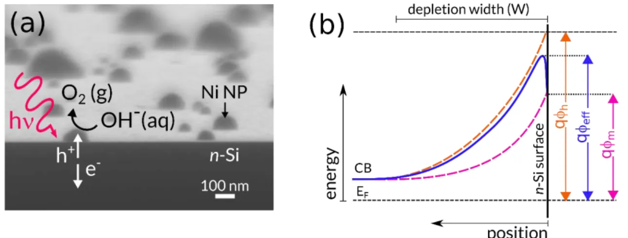
the need for the deposition of a conformal layer. A typical n-Si/Ni NP photoanode produced by this method is shown in Figure 1a. During operation of such systems, a protective SiOx layer at the Si
surface and a hydroxide-oxyhydroxide (M(OH)2-MOOH) shell on the metal NPs grant stability and
promote high OER activity, respectively.32 These photoanodes are described as inhomogeneous
junctions operating in the “pinch-off” regime, as illustrated in Figure 1b.24,35 Herein, a mixed contact
is established between n-Si and i) a low barrier height (qm) region and ii) a high barrier height (qh)
region. Although it has been demonstrated that the low barrier height region results from the metal contact n-Si/M due to Fermi level pinning,29,36,37 the nature of the high barrier height region
(n-Si/SiOx,36 n-Si/M(OH)2,33 n-Si/MOOH37, or n-Si/MOx26) is still discussed in the literature.24,29 It has been
shown that when the characteristic size of the M NP is comparable or smaller than the depletion width (W ~10–1000 nm), the distinct regions act no longer as parallel contacts and the minority carriers experience a higher effective barrier height (qφeff; Figure 1b).34,35 The pinch-off effect is
extremely beneficial because it takes advantage of the qφh region to generate a high photovoltage
and the n-Si/M region to create a low resistance pathway for photogenerated minority carriers, which are readily injected at the catalytic surface for OER (Figure 1a). To date, n-Si/M NPs
photoanodes, such as n-Si/Ni NPs, are only produced by conventional metal electrodeposition.25-31
While this approach is very attractive due to its simplicity and cost, it is based on a process that involves randomly-dispersed nucleation, which does not allow fine control over the geometrical parameters of the nanoscale n-Si/M junction and produces M NPs with a broad dispersion in diameter25 and shape.29,31 By this method, the dimensions of the metal contacts can be hardly
controlled, which is critical for promoting pinch-off and reaching high photoelectrochemical performance. Furthermore, control of the respective spacing between the metallic NPs is difficult.
3
Figure 1. (a) Tilted SEM view of an n-Si/Ni NP photoanode prepared by conventional electrodeposition of Ni on n-Si. The left
part of the panel illustrates the photoanode operation in alkaline pH. Under illumination, holes are directed to the Ni NPs where they participate in the OER reaction. (b) Scheme of the conduction band energy as a function of the position in n-Si in the pinch-off regime (adapted from ref. 34), where qφm is the low barrier height at the metal contact, qφh is the high barrier
height, and qφeff is the effective barrier height.
Lithographically patterned nanowire electrodeposition (LPNE) is a convenient manufacturing process developed by Penner et al.38,39 that has been employed to the electrodeposition of metal nanowires
(M NWs) on dielectrics, such as glass slides40 or polymer films41, to create nanostructured surfaces,
which have been applied in gas sensing42 and capacitors.43 The linear NW geometry is particularly
interesting for photoelectrochemistry applications, because it is expected to promote pinch-off as observed for hemispherical NPs (exemplarily shown in Figure 1a) according to predictions by Tung et
al.44,45
In this article, we used LPNE for the electrodeposition of catalytic transition metal nanowires (M NWs) with high aspect ratio onto photoactive n-Si. We show that this new approach allows a high degree of control over the geometrical features and the spacing of the nanoscale junctions.
Moreover, we demonstrate that this original method can be employed for the design of OER-active and stable photoanodes with high spatial control, and we study the influence of the geometrical parameters on photoelectrochemical OER at n-Si/Ni NWs. We finally employed an electrical modeling approach to qualitatively understand our results. The degree of control provided by this approach has the potential to open up new perspectives for photoelectrodes based on nanoscale n-Si/M junctions.
Results and Discussion
Composition and morphology control of n-Si/M NW surfaces
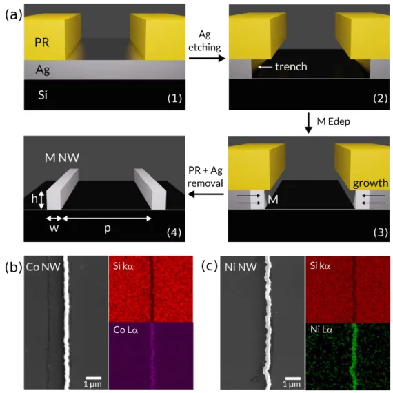
Figure 2a shows the different fabrication steps of lithographically patterned nanowire
electrodeposition (LPNE), which combines the advantages of photolithography, providing control over the structuration of the array at the micrometer scale, with those of electrochemistry, providing the fine-tuning of the dimension of each nanostructure at the nanoscale in a parallel manner.38-40
4
Figure 2. (a) Scheme of the sequential steps of templated electrodeposition for the preparation of catalytic metal
NWs with a high degree of control. The metal growth direction is indicated by black arrows in panel 3, and the geometrical parameters h, w, and p are shown in panel 4. (b,c) SEM top views (left panels) and corresponding Si kα (red), Co Lα (pink), and Ni Lα (green) EDS mapping (right panels) of electrodeposited (b) Co NWs and (c) Co NWs on
n-Si.
First, lightly doped n-Si(100) surfaces (resistivity = 1–10 Ω cm) were covered by a ~80-nm-thick sacrificial Ag thin film and coated by a photoresist (PR) layer that was patterned with stripes over 0.5 x 0.5 cm² by photolithography (Figure 2a, panel (1)). In the following, this surface will be referred to as “template”. Then, the unprotected Ag layer was chemically etched by an NH4OH/H2O2 mixture to
create trenches between the Si substrate and the PR (Figure 2a, panel 2). After that, an electrical contact was established on the Ag layer (note that all Ag stripes were electrically connected
according to Figure S1) for the aqueous electrodeposition of a transition metal M (Figure 2a, panel 3). In this step, electrodeposition is expected to only occur at the surface of the metal layer that is in contact with the electrodeposition bath due to the electrical resistance of the Si wafer and the rectifying nature of the n-Si/Ag junction46 (as a first approximation), i.e., the Ag surface recessed
within the nanoscale trench. This leads to the lateral growth of the metal deposit onto the edges of the silver stripes (black arrows in Figure 2a, panel 3). Finally, the PR is dissolved by acetone, and Ag is selectively etched away, exposing the aligned M NWs on the Si surface (Figure 2a, panel 4). This technique allows the tailored patterning of n-Si with electrodeposited catalytic M NW arrays over a large surface (0.5 x 0.5 cm²). The shape, number, and corresponding pitch (p) of the NWs were
5
controlled by the photomask used to create the template (Figure 2a, panel 1), while the height (h) and width (w) of individual NWs were controlled by the thickness of the sacrificial layer and the electrodeposition parameters (Figure 2a, panel 3). To the best of our knowledge, LPNE has not been previously used on photoactive Si. Furthermore, such a geometry has never been employed for water splitting, even if it has been predicted as promising.44,45
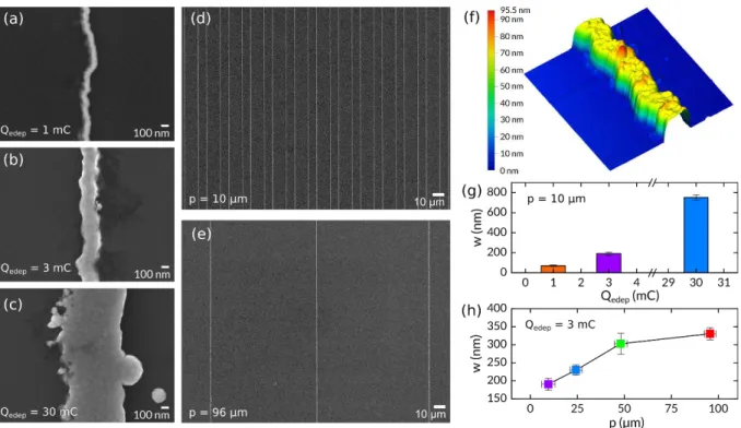
Figure 3. (a–c) High-magnification SEM top view images of Ni NWs electrodeposited on n-Si with p = 10 µm for (a) Qedep = 1
mC, (b) 3 mC, and (c) 30 mC. (d,e) Low-magnification SEM top view images of Ni NWs electrodeposited on n-Si with Qedep = 3
mC for (d) p = 10 and (e) 96 µm. (f) AFM picture (2 x 2 µm²) of a single Ni NWs electrodeposited on n-Si. (g) Graph of w as a function of Qedep for n-Si/Ni NWs prepared with p = 10 µm. (h) Plot of w as a function of p for n-Si/Ni NWs prepared with Qedep
= 3 mC.
To assess the versatility of LPNE, we first tested it for the electrodeposition of the three transition metals (Fe, Co, and Ni). These materials were chosen as they are currently attracting considerable scientific attention as promising inexpensive and efficient catalysts for OER in alkaline medium14 and
also because they are known to yield efficient catalytic inhomogeneous n-Si/M NPs Schottky junctions25,29,30 when electrodeposited as randomly-dispersed NPs on n-Si. The composition of the
electrodeposition baths and the description of the electroplating methods are reported in the Supporting Information. Using LPNE, arrays of aligned Fe, Co, and Ni NWs were successfully obtained on n-Si by applying an electrodeposition charge (Qedep) of 3 mC. Scanning electron microscopy (SEM;
Figure S2) revealed that the NWs had a width in the range of 100 nm, were continuous over long distances, and presented a good adhesion on the substrate. However, the Fe NWs (Figure S2) had an irregular border at one edge (i.e., the NW edge that faced the electrolyte side during
electrodeposition (Figure 2a panel 3)), which was not the case for the better defined Co and Ni NWs, as revealed by SEM (Figure 2b,c). Energy-dispersive X-ray spectroscopy (EDS) was also performed, and the intensity mappings of Si kα and Lα of the deposited transition metals confirmed the chemical nature of the M NWs (top and bottom rows of Figures 2b,c and S2c, respectively). Based on these tests and due to the higher expected stability of n-Si/Ni32 compared to n-Si/Co29 and n-Si/Fe31 OER
photoanodes in highly alkaline solution, we focused on the n-Si/Ni NW system in the following. To evaluate the potential of nanoscale control of LPNE, we fixed the template, which was
6
changed Qedep by controlling the electrodeposition time to vary the Ni NW width. As shown in Figure
3a–c (additional SEM images are shown in Figures S3 and S4a), thin and continuous Ni NWs with a w
value as low as 71 ± 7 nm were obtained by decreasing Qedep to 1 mC (Figure 3g, orange bar). In
contrast, increasing Qedep to 30 mC produced Ni NWs that were more than 10 times wider (w = 751 ±
26 nm; Figure 3g, blue bar). However, to our surprise, applying such a high charge during
electrodeposition also induced the growth of randomly dispersed hemispherical Ni NPs (Figure S3a), which were similar to those obtained for n-Si/Ni NP photoanodes prepared by conventional
electrodeposition (Figure 1a). The origin of the charge-specific nucleation of these NPs is still unclear and is currently under investigation in our laboratory.
In the next experiments, Ni NWs were prepared by applying a constant electrodeposition charge (Qedep = 3 mC) to four different templates, each manufactured using a photomask with PR stripes of
equal pitch and width but with four different values (PR width = PR pitch = 10, 25, 50, or 100 µm). The resulting n-Si/Ni NW surfaces were characterized by SEM (Figure S4). Figure 3d,e shows the results obtained for PR width and pitch of 10 and 100 µm, respectively, revealing that the Ni NWs were properly deposited and continuous over a length of >100 µm. Atomic force microscopy (AFM; Figures 3f and S5) revealed an h value of 80 ± 8 nm. The p and w values of Ni NWs were measured from low and high-magnification SEM images, respectively. Although the width and the spacing of the PR stripes patterned for manufacturing the template were equal, the etching step of the preparation method (Figure 2a, panel 2) inherently induced a break in the p value between
sequential Ni NWs. For the four n-Si/Ni NW surfaces, we experimentally determined p values of 9.6 ± 3.5, 24.3 ± 3.2, 48.1 ± 3.4, and 95.6 ± 3.1 µm, which are referred to by their rounded values (10, 24, 48, and 96 µm, respectively) for simplicity in the following. As h remains constant, and p controls the number of recessed Ag nanobands on the surface, applying a constant Qedep should ideally control
the quantity of electrodeposited Ni atoms and, thus, affect w when using templates with distinct p values. This relation is depicted in Figure 3h, which shows that w increases from 190 to 330 nm for p varying from 10 to 96 µm. Several sets of these surfaces were manufactured, prepared as electrodes, and studied for photoelectrochemical OER.
Figure 4. (a) LSVs (scan rate: 100 mV s-1) of n-Si/Ni NWs in 1 M NaOH with different p values, constant
electrodeposition charge (Qedep = 3 mC), in the dark (black curves), and under illumination (colored curves, average
of >3 independently prepared samples). b) CVs of NiIII/NiII (scan rate: 100 mV s-1) on n-Si/Ni NWs in 1 M NaOH under
illumination. (c) Voc values obtained by OCP measurements in a FeIII(CN)63-/ FeII(CN)64- solution. (d) Plot of QNi as a
function of ANi; squares are experimental data points and the black curve is a linear fit. (e) CA of an n-Si/Ni NW at
2.3 V vs RHE (Qedep = 3 mC, p = 10 µm) in K-borate/Li-borate buffer under illumination. In all panels, the color of the
7
Solar-assisted OER on n-Si/Ni NW photoanodes
As LPNE involves several preparation steps and the use of a sacrificial metal layer, we first had to ensure that any photoelectrochemical activity is only induced by M NWs. To this goal, a control sample was subjected to the same preparation process (Figure 2a) except the Ni electrodeposition step and tested photoelectrochemically, and showed a negligible photoresponse (Figure S10). In contrast, all n-Si/M NW photoelectrodes comprising Fe, Co, and Ni NWs exhibited a clear OER photoelectrochemical activity (Figure S11). These experiments demonstrated the absolute necessity of the presence of the deposited metal on the surface and that the measured activity did not originate from deleterious surface modification or impurities linked to the preparation process. As proof-of-principle comparative experiments, the electrochemical activity of n-Si/Ni NW surfaces prepared with Qedep = 3 mC and p = 10, 24, 48, and 96 µm was studied by voltammetry in 1 M NaOH,
as shown in Figure 4a,b. In the dark, the anodic activity was negligible (black curves). However, the
four surfaces exhibited intense anodic photocurrents when illuminated from the frontside (through the electrolyte) with simulated sunlight (AM 1.5 G, 100 mW cm-2). The photoelectrochemical features
of the n-Si/Ni NW photoanodes are in good agreement with those described for conventional inhomogeneous n-Si/Ni photoanodes.32,36
In particular, the performance of the n-Si/Ni NWs gradually improved during sequential voltammetry cycles (Figure S6) due to the oxidation of the Ni surface to Ni(OH)2-NiOOH and the doping of this
outermost part by catalytically active adventitious Fe atoms.47,48 This phenomenon, which has been
previously reported and studied in detail,32,36 is referred to as “activation”. Unless otherwise
specified, all voltammetry curves reported in this article correspond to the 30th cyclic voltammetry
(CV) cycle. For comparison, the OER activity of the four surfaces is shown in Figure 4a, revealing that their geometrical parameters do not significantly influence the light-limited photocurrent density (jmax). The jmax value was ~33 mA cm-2, which is close to jmax = 31 mA cm-2 obtained from the
incident-photon-to-electron conversion efficiency (IPCE) spectrum recorded at 2 V vs RHE in 1 M NaOH (Figure S7). However, it has a notable influence on the OER slope (the part of the LSV located before the light-limited photocurrent plateau), which increases with decreasing p. This effect can be explained by the overall increase of the Ni surface area that enhances the OER kinetics and also reduces the series resistance of the Schottky junction device. Moreover, Figure 4a,b shows that the OER onset potential increases with p, suggesting that a too low density of Ni NWs and/or a high w is detrimental to the OER performance. However, this activity trend was qualitatively supported by dark/light open circuit potential (OCP) measurements performed in an aqueous solution containing the redox species FeIII(CN)63-/FeII(CN)64- (Figure S8). The results showed that, under these conditions, the photovoltage
(Voc) decreased from 426 to 392 mV with p increasing from 10 to 96 µm (Figure 4c). Another
interesting feature is the quasi-reversible wave that occurred before OER, as shown in Figure 4b for four n-Si/Ni NW photoanodes manufactured with different p values (30th CV cycle). This redox wave
corresponds to the conversion of the outermost NiII(OH)2 layer of the Ni NWs to NiIIIOOH50, and its
magnitude depends on the number of n-Si/Ni NWs on the surface. Figure 4d shows a plot of the anodic charge (QNi; obtained by integration of the region before the forward scan peak) as a function
of the Ni geometric area (ANi), which was calculated using the previously determined geometrical
parameters (Figure 3). These plots showed a linear correlation between these two parameters (R² = 0.982), highlighting the good agreement between photoelectrochemical and characterization data. The slope of the linear fit indicated a charge density of 3.9 ± 0.2 mC cm-2, which agrees relatively well
with the QNi value determined on a 100 nm-thick planar Ni film (4.4 mC cm-2) activated under similar
conditions (Figure S9). The stability of the best n-Si/Ni NW photoanode (p = 10 µm, activated in 1 M NaOH) was tested by chronoamperometry (CA). As shown in Figure 4e, this surface could be operated in a moderately alkaline K-borate/Li-borate buffer (pH = 9.6, which is less basic than 1 M
8
NaOH) at 2.3 V vs RHE for 12 h without loss of performance, delivering an average photocurrent density of 31 mA cm-2, which is very close to the jmax value (33 mA cm-2) determined from the LSVs
shown in Figure 4a. Comparison with data reported on n-Si photoanodes modified by conventional electrodeposition of Ni nanoparticles (Figure S15a)32 showed that these photoanodes have similar
features, although they exhibit a higher OER onset potential and higher jmax. These results showed
that our approach allows for manufacturing stable OER n-Si-based photoanodes with high control over the Ni catalyst geometry and spacing. Moreover, we found that these geometrical features considerably influence the photoelectrochemical performance. Next, we report on our attempts to rationalize the measured photoelectrochemical trends.
Rationalization of the photoelectrochemical trends
The fact that the best performance (Figure 4a), as well as the highest Voc (Figure 4c), was obtained for
the lowest p value is counterintuitive at first. Indeed, as discussed in the introduction, increasing the number of Ni NWs per electrode should increase the area of low barrier height n-Si/Ni contacts (qm;
Figure 1b) and, thus, decrease qφeff in a first approximation, which is correlated to a decrease of the
photoanode performance and opposite to our results. To rationalize our experimental results, we performed 2D electrical numerical simulations applying a finite volume method using the commercial TCAD software Silvaco (details are given in the Supporting Information). These simulations provided the following key photovoltaic parameters: reverse dark current density (j0,dark), short circuit
photocurrent density (jsc), Voc, and fill factor (FF). Our simulations employed a model comprising low
barrier height regions (i.e., n-Si/Ni contacts) spaced by high barrier height regions with the
corresponding work functions (W), which were chosen to define barrier height values in the range reported for metal-covered and metal-uncovered regions.37,51 Even though this latter phase is,
literally, not the liquid because it does not include information about the electrolyte potential, for the sake of simplicity, it is referred to here as the "electrolyte" in the sense that it is the metal-uncovered part of the photoelectrode.
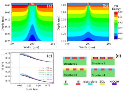
Figure 5. (a,b) 2D representation of the CB energy in n-Si for an n-Si/Ni surface with p =100 µm and (a) w = 350 nm
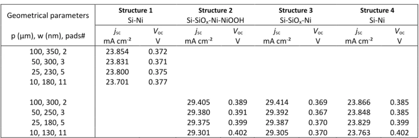
(black) and (b) w = 100 nm. (c) Graph of the band bending below a Ni pad for a surface with p =100 µm for w = 350 (black), 300 (red), 250 (green), 200 (blue), 150 (cyan), and 100 (purple) nm. These energy band profiles are extracted from a cutline located in the middle of the centered Ni pad. Zero depth represents the position of the silicon interface. (d) Schemes of the surface models that have been computed. Their key photovoltaic parameters are reported in Table 1 as a function of their geometrical parameters. The Ni pad electrode widths w of Structures 2, 3, and 4 are reduced by 50 nm compared to those of Structure 1.
9
Table 1. Key photovoltaic parameters extracted from simulated J-V curves under AM 1.5 G illumination for Structures 1-4 shown in Figure 5d.
Geometrical parameters p (µm), w (nm), pads#
Structure 1
Si-Ni Si-SiOStructure 2 x-Ni-NiOOH
Structure 3 Si-SiOx-Ni Structure 4 Si-Ni jsc mA cm-² VV oc mA cmjsc -² VV oc mA cmjsc -² VV oc mA cmjsc -² VV oc 100, 350, 2 23.854 0.372 50, 300, 3 23.831 0.371 25, 230, 5 23.800 0.375 10, 180, 11 23.701 0.377 100, 300, 2 29.405 0.389 29.414 0.369 23.866 0.385 50, 250, 3 29.380 0.391 29.392 0.367 23.848 0.385 25, 180, 5 29.375 0.399 29.387 0.370 23.829 0.399 10, 130, 11 29.301 0.402 29.305 0.370 23.763 0.402
Our first model comprised 3 metal pads (representing Ni NW sections) spaced on a 400 µm-large n-Si surface with w and associated p dimensions that were consistent with our experiments. The results reported in Table S1 demonstrate that the shading effect induced a negligible decrease in the light-limited photocurrent density (which was, in this case, smaller than our experimental jmax values, as
will be discussed later). This also showed that Voc increased with decreasing p and w due to the
change in reverse dark current density (j0,dark) associated with the increasing n-Si/Ni contact area. This
model structure was also used to picture the Si energetics around a Ni pad. Figure 5a,b shows the
models as 2D representations of the conduction band (CB) energy for p = 100 µm and extreme w values of 350 and 100 nm, respectively. These data show the considerable impact of w on the band bending profile close to the surface (see the supplementary information for more details). This is also clearly illustrated in Figure 5c, which shows the 1D band bending (conduction and valence bands) below a Ni pad with a p value fixed at 100 µm and varying pad width (100 nm < w < 350 nm). These figures clearly show that shrinking the Ni NW section increases the effective barrier height, which is in good agreement with the literature devoted to the pinch-off phenomenon.35,44,45 Importantly, the
change of p in the 10–100 µm range had no significant impact on the Si band bending. According to our simulation, an impact will be only observed for p < 0.5 µm (in the range of w used here), which falls below the reachable range of our experimental study.
To better understand the photoelectrochemical results in Figure 4, we tested a set of more sophisticated model structures, shown in Figure 5d. Here, 200 µm-wide n-Si surfaces were entirely covered by metal pads with p/w set values of 100 µm/350 nm, 50 µm/300 nm, 25 µm/230 nm, and 10 µm/180 nm, which were coherent with experimentally determined values (Figure 3h). The values of jsc and Voc of each system are reported in Table 1. The first model that was tested (Figure 5d,
Structure 1) is similar to that used for Figure 5c (see also Table S1) but comprises a higher and more realistic NW surface coverage. Tables 1 and S2 show that this structure exhibited a smaller but coherent evolution of Voc with the geometrical parameters. However, the jsc values (~24 mA cm-2)
were lower than the experimentally determined jmax (31 to 33mA cm-2; Figures 3a and S7). Another
structure model that was computed comprised additional surface oxide layers, namely SiOx and
NiOOH, which are known to appear at the Si and the Ni surface, respectively, during the operation as photoanodes (as discussed previously, Figure 4b).32,50 Here, a 2 nm-thick SiO
x layer and 25 nm-wide
NiOOH layers, present at both edges of the Ni pads, were added to our model (Figure 5d, Structure 2). As shown in Table 1, the modeling results of Structure 2 were in better agreement with our experimental results, and jsc was much higher (~29 mA cm-2) with a stronger Voc increase. Finally, to
10
computed. As illustrated in Figure 5d, these control surfaces were geometrically identical to Structure 2, but Structure 3 did not contain NiOOH, and Structure 4 contained neither NiOOH nor SiOx coating. The results shown in Table 1 demonstrate that Structures 3 and 4 lead to tendencies
that are farther from our experimental results. Indeed, if the presence of SiOx imposes a high jsc
(Supporting Information, Table S3), it does not promote the variation of Voc (~0.37 V). Moreover,
shrinking of the Ni pad width due to the presence of NiOOH improves the Voc trend but does not lead
to relevant jsc values. To sum up, our simulation approach allows us to qualitatively understand the
experimental results obtained in the photoelectrochemical experiments. In particular, it showed that the decrease of the width of the Ni NW due to oxidation to NiOOH is likely a key parameter that increases Voc and thus descreases the onset potential (Figure 4a,b). Conversely, p has a very small
influence on Voc in our length scale. Furthermore, our simulations highlight the importance of the
SiOx layer in promoting a high photocurrent density.
Conclusions
To conclude, we have proposed an original electrodeposition approach for the preparation of tailored inhomogeneous n-Si/M NW Schottky junctions, and we have demonstrated that these surfaces can be used as reliable photoanodes for OER in alkaline solution. This method allows the unprecedented control of the geometrical parameters of nanoscale metal contacts (i.e., Ni, Co, and Fe), which act as hole collectors as wellas catalytically active sites for the electrochemical reaction. Our measurements revealed that the photoelectrochemical properties of the manufactured
photoanodes were strongly dependent on the photoanodes’ geometrical features, and the obtained experimental trends were rationalized by a qualitative simulation approach. In particular, our results are consistent with the existence of a high barrier height region originating from the contact
between n-Si and a metal oxide or oxyhydroxide phase on the NWs. We believe that this
electroplating method has the potential to provide important insights into inhomogeneous pinched-off photoanodes, for which geometric control at the nanoscale is a crucial aspect.34,37 For future
studies, it would be relevant to adapt the process to e-beam lithography methods to electroplate catalysts separated by a shorter distance (<1 µm). Furthermore, elucidating the effect of the plated transition metal will bring considerable progress, which should soon be revealed as this process has proven to be very versatile. With the provided degree of control, this approach has the potential to achieve a deep understanding of physicochemical parameters, which could open new avenues in the development of efficient solar-to-fuel conversion photoelectrodes.
Author Contributions
GL conceived and planned the experiments. OS prepared the templates. KO prepared the samples and performed the experiments. SLG performed the modeling and the numerical simulation with the help of CL. The manuscript was written through the contributions of all authors. All authors have approved the final version of the manuscript.
Conflicts of interest
There are no conflicts to declare.
Acknowledgements
This work was funded by ANR (project EASi-NANO, ANR-16-CE09-0001-01). Loïc Joanny and Francis Gouttefangeas from ScanMAT/CMEBA are warmly acknowledged for SEM analyses. Bruno Fabre and Jean-François Bergamini are also acknowledged for fruitful discussions. ScienceScripts.net is
11
acknowledged for the help with the edition of the manuscript. A part of the microfabrication process has been performed at NanoRennes.
References
N. S. Lewis and D. G. Nocera, Proc. Natl. Acad. Sci., 2006, 103, 15729–15735.
D. Abbott, Proc. IEEE, 2010, 98, 42–66.
H. Gerischer, in Solar Energy Conversion: Solid-State Physics Aspects, ed. B. O. Seraphin, Springer, Berlin, Heidelberg, 1979, pp. 115–172.
M. G. Walter, E. L. Warren, J. R. McKone, S. W. Boettcher, Q. Mi, E. A. Santori and N. S. Lewis, Chem.
Rev., 2010, 110, 6446–6473.
R. van de Krol and M. Grätzel, Photoelectrochemical Hydrogen Production, Springer, New York, 2012. J. W. Ager, M. R. Shaner, K. A. Walczak, I. D. Sharp and S. Ardo, Energy Environ. Sci., 2015, 8, 2811–
2824.
K. Sivula and R. van de Krol, Nat. Rev. Mater., 2016, 1, 15010.
M. S. Prévot and K. Sivula, J. Phys. Chem. C, 2013, 117, 17879–17893.
J. Tournet, Y. Lee, S. K. Karuturi, H. H. Tan and C. Jagadish, ACS Energy Lett., 2020, 5, 611–622.
K. Sun, S. Shen, Y. Liang, P. E. Burrows, S. S. Mao and D. Wang, Chem. Rev., 2014, 114, 8662–8719.
Z. Luo, T. Wang and J. Gong, Chem. Soc. Rev., 2019, 48, 2158–2181.
D. Bae, B. Seger, P. C. K. Vesborg, O. Hansen and I. Chorkendorff, Chem. Soc. Rev., 2017, 46, 1933–
1954.
X. G. Zhang, Electrochemistry of Silicon and Its Oxide, Kluwer Academic, 2001.
C. C. L. McCrory, S. Jung, I. M. Ferrer, S. M. Chatman, J. C. Peters and T. F. Jaramillo, J. Am. Chem.
Soc., 2015, 137, 4347–4357.
S. A. Lee, S. Choi, C. Kim, J. W. Yang, S. Y. Kim and H. W. Jang, ACS Mater. Lett., 2020, 2, 107–126.
K. Jun, Y. S. Lee, T. Buonassisi and J. M. Jacobson, Angew. Chemie Int. Ed., 2011, 51, 423–427.
M. J. Kenney, M. Gong, Y. Li, J. Z. Wu, J. Feng, M. Lanza and H. Dai, Science 2013, 342, 836–840.
18 S. Hu, M. R.Shaner, J. A. Beardslee, M. Lichterman, B. S. Brunschwig and N. S. Lewis, Science 2014, 344, 1005–1009.
Z. Luo, B. Liu, H. Li, X. Chang, W. Zhu, T. Wang and J.Gong, Small Methods 2019, 0, 1900212.
A. G. Scheuermann, J. P. Lawrence, K. W. Kemp, T. Ito, A. Walsh, C. E. D. Chidsey, P. K. Hurley and P. C. McIntyre, Nat. Mater. 2016, 15, 99–105.
I. A. Digdaya, B. J. Trześniewski, G. W. P. Adhyaksa, E. C. Garnett and W. A. Smith, J. Phys. Chem. C 2018, 122, 5462–5471.
X. Zhou, R. Liu, K. Sun, K. M. Papadantonakis, B. S. Brunschwig and N. S. Lewis, Energy Environ. Sci. 2016, 9, 892–897.
12
Y. Li, G. Xu, X. Zhu, Z. Man, X. Fu, Z. Hao, Y. Cui, C. Yuan, W. Zhang, S. Yan, H. Ge, Y. Chen and Z. Zou,
Appl. Catal. B Environ., 2019, 259, 118115.
G. Loget, Curr. Opin. Colloid Interface Sci., 2019, 39, 40-50.
G. Loget, B. Fabre, S. Fryars, C. Mériadec and S. Ababou-Girard, ACS Energy Lett., 2017, 2, 569–573.
S. A. Lee, T. H. Lee, C. Kim, M. G. Lee, M.-J. Choi, H. Park, S. Choi, J. Oh and H. W. Jang, ACS Catal., 2018, 8, 7261–7269.
C.-W. Tung, T.-R. Kuo, C.-S. Hsu, Y. Chuang, H.-C. Chen, C.-K. Chang, C.-Y. Chien, Y.-J. Lu, T.-S. Chan, J.-F. Lee, J.-Y. Li and H. M. Chen, Adv. Energy Mater. 2019, 9, 1901308.
K. Oh, L. Joanny, F. Gouttefangeas, B. Fabre, V. Dorcet, B. Lassalle-Kaiser, A. Vacher, C. Mériadec, S. Ababou-Girard and G. Loget, ACS Appl. Energy Mater., 2019, 2, 1006–1010.
J. C. Hill, A. T. Landers and J. A. Switzer, Nat. Mater., 2015, 14, 1150–1155.
S. A. Lee, T. H. Lee, C. Kim, M.-J. Choi, H. Park, S. Choi, J. Lee, J. Oh, S. Y. Kim and H. W. Jang, ACS
Catal., 2020, 10, 420–429.
K. Oh, V. Dorcet, B. Fabre and G. Loget, Adv. Energy Mater., 2020, 10, 1902963.
K. Oh, C. Mériadec, B. Lassalle-Kaiser, V. Dorcet, B. Fabre, S. Ababou-Girard, L. Joanny, F. Gouttefangeas and G. Loget, Energy Environ. Sci., 2018, 11, 2590–2599.
G. Xu, Z. Xu, Z. Shi, L. Pei, S. Yan, Z. Gu and Z. Zou, ChemSusChem, 2017, 10, 2897 –2903.
R. C. Rossi, N.S. Lewis, J. Phys. Chem. B 2001, 105, 12303–12318.
R. T. Tung, App. Phys. Rev., 2014, 1, 011304.
F. A. L. Laskowski, M. R. Nellist, R. Venkatkarthick and S. W. Boettcher, Energy Environ. Sci., 2017, 10,
570–579.
F. A. L. Laskowski, S. Z. Oener, M. R. Nellist, A. M. Gordon, D. C. Bain, J. L. Fehrs and S. W. Boettcher,
Nat. Mater., 2020, 19, 69–76.
E. J. Menke, M. A. Thompson, C. Xiang, L. C. Yang and R. M. Penner, Nat Mater, 2006, 5, 914–919.
J. E. Hujdic, A. P. Sargisian, J. Shao, T. Ye and E. J. Menke, Nanoscale, 2011, 3, 2697–2699.
C. Xiang, S.-C. Kung, D. K. Taggart, F. Yang, M. A. Thompson, A. G. Güell, Y. Yang and R. M. Penner,
ACS Nano, 2008, 2, 1939–1949.
G. Loget and R. M. Corn, Chem. - A Eur. J., 2014, 20, 10802–10810.
H.-J. Cho, V. T. Chen, S. Qiao, W.-T. Koo, R. M. Penner and I.-D. Kim, ACS Sensors, 2018, 3, 2152–2158.
M. Le Thai, G. T. Chandran, R. K. Dutta, X. Li and R. M. Penner, ACS Energy Lett., 2016, 1, 57–63.
R. T. Tung, Appl. Phys. Lett., 1991, 58, 2821–2823.
J. P. Sullivan, R. T. Tung, M. R. Pinto and W. R. Graham, J. Appl. Phys., 1991, 70, 7403–7424.
R. Balsano, A. Matsubayashi and V. P. LaBella, AIP Adv., 2013, 3, 112110.
13
M. B. Stevens, L. J. Enman, A. S. Batchellor, M. R. Cosby, A. E. Vise, C. D. M. Trang and S. W. Boettcher, Chem. Mater., 2017, 29, 120–140.
S. L. Medway, C. A. Lucas, A. Kowal, R. J. Nichols and D. Johnson, J. Electroanal. Chem., 2006, 587,
172–181.
D. S. Hall, C. Bock and B. R. MacDougall, J. Electrochem. Soc. , 2013, 160, F235–F243.
G. Loget, C. Mériadec, V. Dorcet, B. Fabre, A. Vacher, S. Fryars and S. Ababou-Girard, Nat. Commun.