HAL Id: hal-03043725
https://hal.archives-ouvertes.fr/hal-03043725
Submitted on 7 Dec 2020HAL is a multi-disciplinary open access
archive for the deposit and dissemination of sci-entific research documents, whether they are pub-lished or not. The documents may come from teaching and research institutions in France or abroad, or from public or private research centers.
L’archive ouverte pluridisciplinaire HAL, est destinée au dépôt et à la diffusion de documents scientifiques de niveau recherche, publiés ou non, émanant des établissements d’enseignement et de recherche français ou étrangers, des laboratoires publics ou privés.
Mechanical stress in InP and GaAs ridges formed by
reactive ion etching
Jean Pierre Landesman, Marc Fouchier, Erwine Pargon, Solène Gérard,
Névine Rochat, Christophe Levallois, Merwan Mokhtari, Philippe
Pagnod-Rossiaux, François Laruelle, Camille Petit-Etienne, et al.
To cite this version:
Jean Pierre Landesman, Marc Fouchier, Erwine Pargon, Solène Gérard, Névine Rochat, et al.. Me-chanical stress in InP and GaAs ridges formed by reactive ion etching. Journal of Applied Physics, American Institute of Physics, 2020, 128 (22), �10.1063/5.0032838�. �hal-03043725�
Mechanical stress in InP and GaAs ridges formed by reactive ion etching
Jean-Pierre Landesman,1, a) Marc Fouchier,2, b) Erwine Pargon,2 Solène
Gérard,3, c) Névine Rochat,4 Christophe Levallois,1 Merwan Mokhtari,3, c) Philippe
Pagnod-Rossiaux,5 François Laruelle,5 Camille Petit-Etienne,2 Mauro Bettiati,5 Juan
Jiménez,6 and Daniel T. Cassidy7
1)Univ Rennes, INSA Rennes, CNRS, Institut FOTON—UMR 6082,
F-35000 Rennes, France
2)Univ. Grenoble Alpes, CNRS, CEA/LETI-Minatec, Grenoble INP, LTM, F-38054 Grenoble-France
3)Univ Rennes, CNRS, IPR – UMR 6251, F-35000 Rennes,
France
4)Univ Grenoble Alpes, CEA-LETI, F-38000 Grenoble, France
5)3SP Technologies S.A.S, F-91625 Nozay, France
6)Dpto. Fisica de la Materia Condensada, Universidad de Valladolid, 47011 Valladolid, Spain
7)McMaster University, Department of Engineering Physics, Hamilton, ON L8S 4L7, Canada
The mechanical deformation induced by reactive ion etching (RIE) of rectangular ridge waveguides in GaAs and InP has been investigated by photoluminescence and cathodoluminescence techniques. Several trends were identified and are discussed. First, it is concluded that the RIE process itself is the source of the mechanical de-formation. A compressive volume change occurs mainly within the ridge (with a maximum close to the vertical etched sidewalls), extending outside the ridges, up to several µm below the bottom etched surface. An anisotropic deformation also appears, again mainly close to the etched sidewalls and below the bottom etched surface. A narrow area under tensile stress was also identified, localized outside the ridges and in a shallow region below the bottom etched surface. Cumulative, overlap-ping effects are seen, inside the ridges where the compressive stress fields originating at the vertical etched sidewalls contribute to an overall compression inside the ridge which increases as the ridge width decreases. In addition, a tensile stress is also ob-served outside the ridge, strongly enhanced by the presence of neighbouring ridges. These conclusions are significant for the design of photonic structures. Because of the photoelastic effect, which is important in GaAs and InP, the properties of devices such as waveguides might be affected by the mechanical stress described herein. PACS numbers: 42.79.Gn, 42.82.Cr, 52.77.Bn, 61.72.uj, 62.20.F, 78.55.Cr, 78.60.Hk Keywords: Reactive ion etching, Photoluminescence, Cathodoluminescence, Mechan-ical stress
a)Electronic mail: Jean-Pierre.Landesman@univ-rennes1.fr. b)Present address: Attolight AG, 1015 Lausanne, Switzerland. c)Present address: 3SP Technologies S.A.S, F-91625 Nozay, France.
I. INTRODUCTION
Reactive ion etching (RIE) is one of the ubiquitous processes contributing to the devel-opment of nanotechnology platforms, whether it is for the fabrication of electronic, opto-electronic or photonic components and integrated circuits. The fundamental mechanisms involved in RIE pertain to plasma physics, to interactions of surfaces with energetic ions and reactive species, and also to modifications of the bulk materials properties by these reac-tants. Optimisation of RIE in a process flow can be complex due to the choice of the possible adjustable parameters (starting with the type of reactive and dilution gases, along with the choice of the type of plasma reactor, the power applied to the plasma source, the sample temperature, possibly the power at the secondary radio-frequency (RF) source to adjust self–bias, choice of the masking material ...1,2). In the simplest optimization procedure, the
selection of parameters can be made looking at the geometrical shape, critical dimensions, and residual roughness of the resulting etched nanostructures. However, considering the trend towards reduced dimensions and the fact that the active areas in the semiconductor material are getting closer to the etched surfaces, careful control of changes induced in the materials properties in the proximity of etched surfaces also needs to be considered.
Schematically, three kinds of disorder induced by plasma etching have been reported in the literature3:
• chemical disorder (such as non-stoichiometry in materials like GaAs and InP);
• crystallographic disorder (creation of amorphous layers, atomic displacements through collision cascades, ...) and
• creation of point defects affecting the electronic or optical properties.
State-of-the-art photonic integrated circuits based on InP are good examples of how the etching process can impact the resulting performances. Fandino and Munoz4 show that an
error of±0.1 µm on the width of the rib waveguides used to generate multimode interference (MMI) couplers could lead to a decrease of the bandwidth by a factor of 4 (from 40 to 10 nm). The integrated circuits discussed in4 are designed for high speed coherent optical
communications around 1550 nm. The nominal width for the MMIs was 40 µm. Similarly, manufacturing deviations on the shape of the ribs (e.g. non vertical lateral walls) would also significantly affect the performance of such devices. The etch roughness can also generate
optical losses, as shown in the case of InP/InGaAsP waveguides with integrated mirrors to ensure 45◦ bends to the propagating mode5.
Plasma etching of GaAs and InP can induce a depletion of the element V6. It can also
produce damage to the crystal structure, which can be identified either directly using high resolution transmission electron microscopy6, or through the use of optical techniques such
as photoluminescence (PL), for example to measure Fabry-Perot damping in waveguides7.
A number of groups have also investigated the generation of electrically active defects in GaAs and InP by plasma etching (e.g.8,9). It has been shown that under the conditions
used for plasma etching of GaAs and InP, these effects (especially electrically and optically active defects) can reach distances up to hundreds of nm beneath the surface because of the possibility for ions to channel through the crystals10–12.
In this article, we propose a different approach to investigate modifications to the semi-conductor material during plasma (RIE) etching of GaAs and InP-based structures: we focus on the analysis of the presence of mechanical deformation by means of spatially re-solved luminescence techniques (either optical excitation (PL) or electron beam excitation cathodoluminescence (CL)). The motivation to investigate crystal deformation comes from the idea that some of the effects reported for plasma etching can introduce local strains. In particular, this is the case if ions or fast neutral radicals channel through the crystal lattice and stop at some depth once they have transferred their energy. Non-stoichimetric surfaces, resulting from the depletion of the element V, might also generate strain if the non-stoichiometric material extends over depths of 10 nm or more13. On the other hand, this
study is also motivated by the consideration that residual mechanical stress would affect the optical properties of photonic devices because of the photoelastic effect, which can be critical in the case of a waveguide fabrication. The impact of mechanical stress on waveguides has been described in details by Huang14. Photoelasticity is strong in III-V compounds15, and
consequently mechanical stress for such materials can lead to multimode operation, birefrin-gence, or changes of the shape of the optical mode, possibly resulting in additional optical losses14.
This article is organized as follows: the details of interest for the experimental part (sam-ple preparation, plasma etching processes and measurement techniques) are described in section 2. Section 3 lists the results obtained using the different approaches of our experi-mental techniques and the different sample geometries. Section 4 presents a discussion of the
results including data fitting with a simple analytical model and preliminary finite element simulations aiming at testing some ideas about the localization of the defects generated during plasma etching. Section 5 concludes the work.
II. EXPERIMENTS
A. Samples
We have used bulk GaAs and InP wafers, with (100) orientation. All the samples were n-type doped in the order of 1018 cm−3. Rectangular ridges aligned along the ⟨110⟩ direction
were etched on the surface of the wafers. A SiNx hard mask thin film was deposited by
plasma enhanced chemical vapor deposition (PECVD) for the definition of these structures. Different PECVD reactors and different gas mixtures were used to deposit the mask layers. The deposition temperature for the SiNx films was typically in the range [250 ◦C - 300 ◦C]
and the thickness was 500 nm. Before etching of the semiconductor material to form the rectangular ridge, the films were patterned by standard or electron beam lithography to different widths (from 0.5 to 20 µm) followed by opening using RIE etching with SF6 or
CF4/O2 plasmas.
B. Plasma etching processes
Different nanotechnology platforms for the etching of the semiconductor material (either GaAs or InP) were used:
• Process #1 involved CH4 (6.4 sccm) /H2 (50 sccm) /Ar (8.4 sccm) in a capacitively
coupled RIE reactor. The total pressure was 30 mTorr and the RF power was 40 W. In this process the sample is attached to a water-cooled sample holder (water temperature between 10 and 15 ◦C). The DC self-bias for this process was −360 V . • Process #2 involved CH4 (32 sccm) /Cl2 (20 sccm) /Ar (100 sccm) in an inductively
coupled RIE reactor. The total pressure was 20 mTorr and the RF power was 800 W at the plasma source and 200 W for sample bias. The sample holder controlled temperature was 200 ◦C. The DC self-bias for this process was−375 V .
Processes #1 and #2 were used to etch InP, and process #3 was used for GaAs etching. After the semiconductor etching step, the organic contamination was eliminated in an O2
plasma and the remaining SiNx was removed using HF wet etch. This ensures that the
effects investigated are due solely to the reactive ion etching procedure.
C. Measurement techniques
To characterize and map the local mechanical deformations in our samples we used local probe luminescence techniques. A description of the application of PL and CL for mapping local stresses and strains in III-V semiconductor materials and devices can be found in16for
example. We provide a synopsis of our implementation of these techniques as follows: • The spectral shift of the (spectrally resolved) luminescence line associated with
band-to-band transitions in bulk III-V semiconductors is linked to the local volume change in the absence of doping modifications. Details on the formulation and case applications can be found in16,17.
• The degree of polarization (DOP) of the spectrally integrated luminescence is related to the deformation anisotropy and shear deformation in the plane perpendicular to the optical beam, as established by Cassidy and co-workers18.
Recent results illustrating these approaches, as well as detailed formulations, can be found in19–21. In this paper, we discuss results obtained from the spectral shift of the intrinsic
CL emission (SS-CL), the degree of polarization of the PL (DOP-PL), and the degree of polarization of the CL (DOP-CL) intrinsic emission. The main difference between PL and CL is the spatial resolution and the field of view. In PL the spatial resolution is limited by diffraction to approximately 1 µm, making details smaller than this difficult to resolve. On the other hand, it is possible with PL to scan over distances of several hundred microns. In CL, the spatial resolution (determined by the extension of the electron beam / sample interaction volume and the carrier diffusion length) can be as good as 100 nm depending on the acceleration voltage22, however, the lateral extension of the images is limited to a few
microns. The PL measurements were performed using a 635 nm excitation laser, while a 5 kV electron acceleration voltage was used for the CL measurements.
The samples were scanned on both the top (100) surface across the etched ridges and a cleaved (110) surface in the area of the etched ridges.
III. RESULTS
A. (110) Cross sectional mappings
Fig. 1 shows CL cross sectional maps for a 6 µm wide ridge etched over 3 µm deep in InP (etch process #2). Fig. 1-a is the SS-CL map in the area of the ridge. To convert the
FIG. 1: CL maps on the cross-section of an InP ridge etched with process #2 (CH4/Cl2/Ar). Width: W = 6 µm; etch depth: d = 3µm. (a) : volume change deduced
from SS-CL; (b) : DOP-CL.The color scale on the right gives respectively the relative volume change and DOP-CL.
spectral shift to a volume change, the following formula was used21:
∆E(meV) =−6.15 × 10³· (ϵxx+ ϵyy + ϵzz) (1)
This relation between the spectral shift ∆E and the volume change (ϵxx + ϵyy + ϵzz) was
established based on the deformation potentials given by23. Computing the volume change
requires knowledge of the CL peak position for unstrained material. A CL spectrum recorded in the bulk InP, far below the (100) surface, was used as a reference. The volume deformation appears compressive over the entire area displayed in fig. 1-a, decreasing towards the bulk. The compression remains significant up to 2 or 3 µm below the etched surface, and also in the whole area within the ridge.
Fig. 1-b is the DOP-CL map in the same area. The DOP measured from a (110) surface is defined as DOPy= Ix− Iz Ix+ Iz (2) where Ix is the component of the spectrally integrated CL signal with polarization parallel
to the x axis of fig. 1-b18. z is along [100], x is along [¯110] and y is along [110]. The
DOP originates from an anisotropic deformation of the crystal which initially has cubic symmetry. Cassidy et al.18 have established that, in a first approximation, the DOP signal
is proportional to the difference in the normal strain coefficients along the 2 axes in the plane of observation. They proposed the formula
DOPy=−CDOP(ϵxx − ϵzz) (3)
for a (110) surface, with CDOP = 65± 10 for InP(110) and CDOP = 50± 10 for GaAs(110),
applicable for DOP-PL measurements (we consider these to be applicable to DOP-CL mea-surements as well). According to this formula, a positive DOP signal as shown on fig. 1-b means that the deformation is more compressive (or less tensile) in the x direction than in the z direction. Note that the measured DOP signal is low (a few % maximum).
Recent theoretical work24indicates that the relation between the DOP and the normal strain
coefficients might be more complex than given by eq. 3 for a (110) surface, due to the loss of square symmetry. We have kept the DOP values for the scale in DOP maps instead of converting them to (ϵxx− ϵzz).
Fig. 1-b shows that the DOP signal is positive (indicated in blue on the color map) in the area next to the vertical etched walls, and negative (red on the color map) below the bottom etched surface. This could indicate a dominant compressive strain along x close to the vertical etched walls, and a dominant tensile strain along x (or compressive strain along
z) close to the bottom etched surface.
Fouchier20 established a correction procedure for the signal from SS-CL and DOP-CL in
areas very close to the different surfaces on the sample. However, this procedure requires complex additional measurements and could not be applied for the CL results presented in this paper. CL data for points located less than 1 µm from the surfaces should be considered with some restriction. Nevertheless, the trends observed extend significantly beyond this 1
µm thick layer.
etch process, same depth as for fig. 1) are shown in fig. 2. The magnitudes of the CL
FIG. 2: CL maps on the cross-section of InP ridges of different widths etched with process #2 (CH4/Cl2/Ar). d = 3µm. (a) : SS-CL / W = 3 µm, (b ): DOP-CL / W = 3 µm, (c) :
SS-CL / W = 1 µm, (d) : DOP-CL / W = 1 µm.
and DOP signals increase inside the ridge as the width decreases from 6 to 3 and 1 µm, indicating a cumulative effect on the crystal deformation when the vertical etched sidewalls get closer to each other. The SS-CL and DOP-CL signals, on the other hand, remain similar below the bottom etched surfaces.
B. (100) top surface measurements
We now describe the results obtained by recording PL and CL from the top (100) surface. Since the ridges are elongated along the y direction (elongation: a few mm) we only present linescans along the x direction (across the ridges) instead of maps in the xy plane. Linescans
recorded along the x direction do not show any change as a function of the y coordinate as long as the measurement area is far enough from the edge ends. This allows us to average
x direction linescans for different y values, thus improving the signal - to - noise ratio. Note
that the DOP signal is now measured for the optical beam propagating along the z direction.
1. Spectral shift cathodoluminescence (SS-CL)
Fig. 3 shows (100) surface SS-CL linescans across two of the ridges similar to those of figs. 1 and 2. Note that the measured spectral shift in fig. 3 was not converted into a volume deformation. The reason for this is that the sample is not planar owing to the presence of ridges. The strain can be assumed independent of the y coordinate along the [110] direction (measurement geometry for figs. 1 and 2) but this is not the case along the z coordinate in the [100] direction (measurement geometry for fig. 3). The peak shifts in fig. 3 are a weighted average of the crystal deformation over the depth probed by the CL signal (a few hundred nm). Fig. 3 indicates compressive deformation inside the ridges, and tensile deformation just outside the ridges, returning to zero a few microns away from the ridge. The apparent discontinuity at the ridge edges is not an artefact. It arises from the fact that the scanned region inside the ridge lies near the top surface, whereas it lies near the bottom etched surface outside the ridge25. The etch depth (3 µm) is much larger than the depth
probed in InP by the 5 kV electron beam in the CL measurement.
Comparing the two curves in fig. 3 one can observe that the compressive strain inside the ridge is significantly higher for the 1 µm ridge than for the 6 µm one, which is qualitatively similar to what was revealed by the cross section scans. Fig. 3 also evidences an area under tensile strain just outside the ridge edges. This is apparently different from the trends shown on figs 1 and 2 where the volume change is compressive everywhere. However, it should be noticed that the depth probed in the surface scans (fig. 3) is a few hundred nm at most. This zone below the surface is too small to be clearly identified on the cross section scans.
2. Degree of polarization of the photoluminescence (DOP-PL)
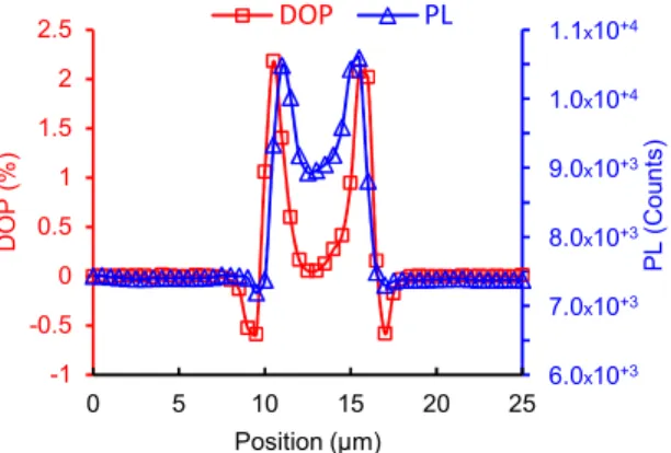
A PL linescan across a 6 µm ridge in InP can be seen in fig. 4 (the DOP-PL and PL intensity signals are superimposed). The sample was etched to a depth of 0.5 µm using
-10 -5 0 5 10 15 0 20 40 P e a k s h if t (m e V ) Position (µm) W=1 µm W=6 µm
FIG. 3: SS-CL profile across the surface of isolated ridges etched in InP : W = 1 µm and
W = 6 µm, d = 3µm. Etch process: CH4/Cl2/Ar.
process #1. Taking into account the fact that the ridge length is in the mm range, we can assume that the strain ϵyy along this length is negligible. Indeed, any non-zero ϵyy should be
almost constant along the ridge since the length can be considered infinite. This would induce an overall curvature of the sample in the y direction21. Such curvature was not observed
6.0x10+3 7.0x10+3 8.0x10+3 9.0x10+3 1.0x10+4 1.1x10+4 -1 -0.5 0 0.5 1 1.5 2 2.5 0 5 10 15 20 25 P L ( C o u n ts ) D OP ( % ) Position (µm) DOP PL
FIG. 4: DOP-PL and PL intensity linescans across an isolated ridge etched in InP :
W = 6 µm, d = 0.5 µm; etch process: CH4/H2/Ar.
by profilometry on our samples. Under this assumption, the DOP-PL signal measured from the top (100) surface, which should be −CDOP(ϵxx− ϵyy), reduces to −CDOP· ϵxx. Fig. 4
indicates a compressive transverse strain ϵxx within the ridge, with maxima at the edges,
due to the different zones probed in the material when the laser beam is within the ridge (excitation at the un-etched surface) and outside the ridge (excitation at the bottom etched surface). Fig. 5 is similar to fig. 4 but for a 30 µm ridge. The trend for the DOP-PL signal is the same. The DOP clearly returns to zero over a large central part of the ridge. Fig. 6
2.0x10+3 2.1x10+3 2.2x10+3 2.3x10+3 2.4x10+3 2.5x10+3 2.6x10+3 -1 -0.5 0 0.5 1 1.5 2 2.5 0 5 10 15 20 25 30 35 40 45 50 P L ( C o u n ts ) D OP ( % ) Position (µm) DOP PL
FIG. 5: DOP-PL and PL intensity linescans across an isolated ridge etched in InP :
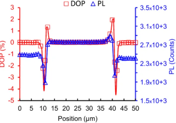
and fig. 7 show the DOP-PL and intensity linescans across ridges of widths 6 and 30 µm etched over 1.6 µm deep in InP, and fig. 8 shows a comparison of the DOP-PL linescans for the 2 different etched depths. The comparison in fig. 8 yields a higher tensile strain just
1.0x10+3 1.4x10+3 1.8x10+3 2.2x10+3 2.6x10+3 3.0x10+3 -5 -4 -3 -2 -1 0 1 2 3 0 5 10 15 20 25 P L ( C o u n ts ) D OP ( % ) Position (µm) DOP PL
FIG. 6: DOP-PL and PL intensity linescans across an isolated ridge etched in InP :
W = 6 µm, d = 1.6 µm; etch process: CH4/H2/Ar.
1.5x10+3 1.9x10+3 2.3x10+3 2.7x10+3 3.1x10+3 3.5x10+3 -5 -4 -3 -2 -1 0 1 2 3 0 5 10 15 20 25 30 35 40 45 50 P L ( C o u n ts ) D OP ( % ) Position (µm) DOP PL
FIG. 7: DOP-PL and PL intensity linescans across an isolated ridge etched in InP :
W = 30 µm, d = 1.6 µm; etch process: CH4/H2/Ar.
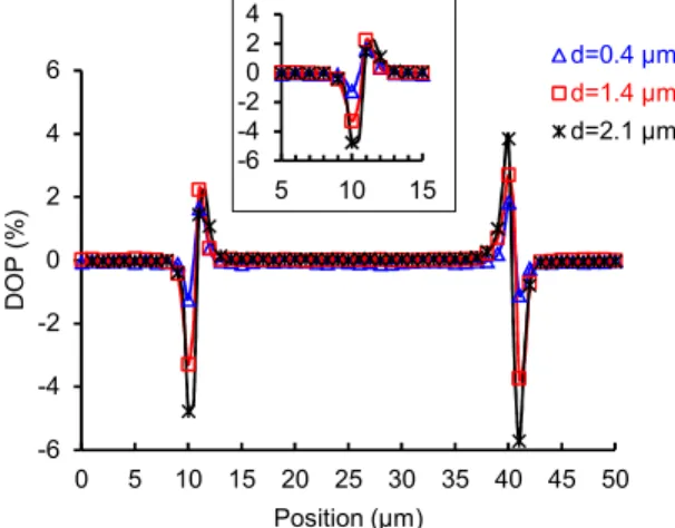
the ridge area does not change. Based on all the DOP-PL measurements that we performed on InP samples, no significant difference could be observed between the etching processes #1 and #2. Finally, fig. 9 illustrates the same trend as fig. 8 for etching in GaAs (process #3): no change inside the ridge, tensile strain outside the ridge, increasing with the etched
depth.
The SiNx mask layer can induce mechanical stress after the PECVD deposition process21.
This mechanical stress can be controlled by changing the PECVD conditions. We have checked (fig. 10) that this state of mechanical stress inside the SiNx mask layer does not
affect the DOP profiles after etching and removal of the mask. The strain in and around the ridges is caused by the semiconductor etching process itself. There is no “memory effect” due to the SiNx mask. This is further evidenced in fig. 11 which compares the DOP profile
induced by a SiNx mask (prior to GaAs etching) and the DOP profile in the GaAs after
etching and mask removal. The strain profiles are clearly different.
3. Proximity effects
The previous results concerned isolated ridges. When neighbouring ridges are close enough, the net strain field, which by the principle of linear superposition is the sum of the contributions from all ridges, increases in the region between the ridges. In fig. 12 one can see the strain measured across the ridge (width 1 µm) and in the spacing between neighbouring ridges (called “trench” on the figure). A semilogarithmic representation is used for fig. 12, and only a half of the 1 µm wide ridge is shown. The curve for the isolated case is the same as in fig. 3. The other curves are for neighbouring ridges with decreasing trench spacing. The compressive strain within the ridge does not seem very much affected by the spacing. However the tensile strain in the trench increases as the spacing decreases. A plateau is observed for the narrowest trenches, showing that the strain fields from both neighbour ridges overlap. An additional feature needs to be taken into account in this dis-cussion of the proximity effects: the dependence of the etching rates on the aspect ratio26.
This reduces the etch depth in areas where the ridge density is higher. Because of this trend, the etch depth between neighbouring ridges with spacing 1 µm can be lower than the etch depth in completely open areas. Typically a reduction of the etch depth from the nominal 3 µm to 2.3 - 2.5 µm could occur for the 1 µm spacings. However, fig. 12 indicates that the areas with the smallest spacings display the strongest tensile stress, which cannot be a consequence of the aspect ratio dependent etch rate (according to which areas with the smallest spacings should display lower stress than areas with largest spacings). In view of this additional comment, the trend illustrated by fig. 12 is indeed a proximity effect
affect-ing the tensile stress in trenches. Fig. 13 illustrates the measured strain profile when the spacing between neighbouring ridges is constant and the ridge width is varied between 0.5 and 6 µm. The overlapping effect is now also identified inside the ridges: within the largest ridge the compressive strain returns to zero in the center, whereas for the narrow ridges the compressive strain shows higher maximum amplitude at the edges, and the decrease is much reduced (in fact, for the 0.5 µm ridge, this compressive strain appears constant over the volume of the ridge). This effect inside the ridge was already observed on the cross section mappings in fig. 2. Fig. 13 (b) also indicates that for a 1 µm spacing the tensile stress within the trenches increases as the width of the ridges increases. Figs. 12 and 13 demon-strate an overlapping effect between neighbouring ridges, which increases when the spacing in between decreases. An overlapping effect is also observed inside the ridges, between the 2 etched sidewalls.
IV. DISCUSSION
The results described provide evidence of the mechanical deformation induced in the semiconductor material by the RIE process. As already stated, the different types of dis-order mechanisms described for plasma etching could generate this mechanical effect: non-stoichiometry, crystallographic disorder or point defects. To start investigating the possible mechanisms we did some numerical simulations of our data. For the (100) top surface measurements, we performed best fit calculations using an analytical model, based on the approach that we developed21 to analyze strain / stress effects induced by the presence of a
SiNx stripe at the surface. In the present work, the strain owing only to RIE is investigated.
In the case treated in21, the effects were due to the residual mechanical stress in the dielectric
films after PECVD, combined with the structuration of the films to form stripes of variable widths. The analytical model was built on the edge force concept27. For the (110) cross
section maps, we performed finite element simulations to test some assumptions, without carrying out any best fit procedure.
A. Analytical fits
The edge force concept was introduced by Hu27 to account for the effects of geometrical
discontinuities in a thin film structure under mechanical stress at the surface. The edge force generates a mechanical stress field with a “slowly” decreasing behaviour away from the discontinuities (application points for the edge forces). In fact, what “slowly” means can be seen on the curves in fig. 11 : the DOP generated at the edges of the stripe owing to the SiNx mask layer is still significant at distances several tens of µm away from the edges.
See21 for a detailed discussion of these effects. On the other hand, the DOP and SS-CL
linescans measured across the etched stripes with no SiNx overlayer show sharp decreasing
effects. These effects cannot be described within the framework of the edge force concept. We used a simple exponential model, with the following adjustable parameters:
• Characteristic 1
e decreasing length inside the ridge, at both edges;
• Characteristic 1
e decreasing length outside the ridge, at both edges;
• Maximum amplitude inside the ridges (at both edges); • Maximum amplitude outside the ridges (at both edges); and,
• 2 “weight” parameters to simulate the effects of the limited spatial resolution without performing a complete convolution procedure (only for the PL linescans, whereas the spatial resolution is not limited for CL linescans).
Fig. 14 illustrates this best fit procedure for a DOP-PL linescan across a 30 µm wide ridge etched in GaAs. The 1
e decreasing lengths for the exponentials are of the order of 0.5 µm,
smaller than the spatial resolution for PL measurements. It is therefore not possible to discuss the values of the decreasing lengths obtained from best fits to the DOP-PL data. However, the amplitudes will show a trend when the etch depth increases (see fig. 9 for example). For etch depths 0.4 / 1.4 / 2.1 µm in GaAs, the best fit yields amplitudes for the exponentials outside the ridge of −1.6 / − 4 / − 4.5 units, and 2 / 3.4 / 4.2 units inside the ridge, indicating increasing ϵxx on both sides of the etch walls as the depth increases.
Figs. 15 and 16 illustrate the best fit for SS-CL linescans across 1 and 6 µm ridges etched in InP (etch depth 3 µm). The characteristic decreasing length inside the ridge is of the order of 0.5 µm, which is larger than the spatial resolution for the CL linescans. Outside the
ridge the decreasing length is 1.3 / 1.4 µm. The values are similar for the different widths investigated. Unfortunately, we were not able to perform the SS-CL linescan measurements for different etch depths.
This analysis of the top surface data leads to the conclusion that in an area close to the surface in the depth probed by PL and CL (between 100 and 500 nm) the strain resulting from etching is concentrated near the vertical etched walls, with a sharp exponential decrease away from these edges, on both sides of the wall. The strain is compressive inside the ridge, and tensile outside. The 1
e decreasing length for ϵxx (deduced from the DOP-PL data) is
below the spatial resolution, i.e., smaller than 1 µm. The maximum amplitude of ϵxx at the
etched walls (on both sides, compressive inside and tensile outside) increases with increasing etched depth which might be expected due to a longer exposure to the etching process. The decreasing length for the volume change (deduced from the SS-CL data) is in the order of 0.5 µm inside the ridge, and slightly higher (1.3 to 1.4 µm) outside.
B. Finite element simulations
The approach to discuss the results from the cross section maps was different than for the top surface scans but informed by the analysis of the top scans: using a finite element simulation tool we generated maps of the volume change (ϵxx + ϵyy + ϵzz) and of the DOP
signal (cf eq. 3) starting from trial assumptions on defect distributions within the etched crystal. A trial assumption was characterized by a spatial distribution of initial strain in the neighbourhood of the different surfaces (vertical etched sidewalls, horizontal bottom etched surface), representing the effects of a defect distribution. The simulation was operated in a stationary configuration, using the solid mechanics / linear elasticity Comsol Multiphysics module, in 2 dimensions (plane strain condition). Standard free surface conditions and prescribed displacements were used. Here, we did not operate any best fit procedure, we just compared qualitatively the simulation results with the experimental maps. Fig. 17 shows the “best agreement” obtained, following this procedure, trying to reproduce the experimental data in fig. 1. This simulation corresponds to the following initial strain distribution:
• Non-uniform isotropic compressive volume change extending from the vertical etched sidewalls, in an oblique direction (45 ◦), with exponential attenuation (1
length: 1 µm). At the sidewalls themselves, the compressive volume change decreases linearly from 5× 10⁻³ at the top 0 at the bottom corners. This linear variation
repre-sents the decreasing exposure to ion bombardment from top to bottom as the etching proceeds. The extension of the volume change starting from the sidewall, in an oblique direction, with exponential attenuation, was chosen to represent the impact of ion and fast neutral radical trajectories inside the material and the ion and neutral radical stopping range.
• Anisotropic vertical compression extending exponentially from the bottom etched sur-face towards the bulk, with 1
e attenuation length 1 µm and maximum 5×10
-3. This was
chosen to represent the propagation of defects resulting from etching of the horizontal surfaces.
The agreement between experimental and simulated maps is acceptable for the volume change on the vertical etched walls and bottom etched surfaces. The agreement is not very good at the bottom ridge corners. This might be explained by more complex ion trajectories in these areas, however we did not attempt to include these details in our simulation. A careful observation of the secondary electron images might be necessary to guess the initial strain distribution in the corners area. The volume change near the top unetched area was not reproduced either in our simulation. We might have included an initial strain in this area to reproduce the experimental trend, but this initial strain would not be related to effects of the ion bombardment induced by the etching process (the top surface being protected by the hard mask layer). We therefore leave this issue for a different discussion.
The agreement for the DOP maps is acceptable.
The analysis of the cross section data (both experimental and simulated maps) indicates that the crystal deformation probably has several origins. A concentration of defects near the vertical etched sidewalls, inducing both an isotropic volume change (propagating in an oblique direction with exponential attenuation) and an anisotropic DOP signal, seems to explain the deformation seen in these areas. This concentration of defects decreases from top to bottom of the ridge, which can be understood in terms of total exposure to ion bombardment during the etch process. We assume that the defects responsible for the crystal deformation near the vertical etched sidewalls are related to ion and radical penetration. A concentration of defects in areas close to the bottom etched surface is also
probably present, explaining the volume change and DOP signal. These defects seem to generate an anistropic crystal deformation, dominant in the vertical direction. Actually we do not have any indication on the physical origin of this deformation (ion bombardment, non stoichiometric surface, ...).
C. Summary of the observations and results
Before the general conclusion, we summarize our observations and comments:
• The cross sectional investigations by CL provide evidence that the etching process induces mechanical stress inside and close to the ridges; in particular, the change in amplitude of the effects (spectral shift and DOP) as a function of reducing ridge width contributes to this important statement. We have pointed out that the CL data processing for areas close to the sample surface is a delicate task for cross sectional maps20 but the effects discussed occur far enough from these surfaces to make valid
observations and conclusions. The cross section maps demonstrate a cumulative effect between strain fields whose origins lie at the two vertical etched walls. An important observation is the compressive stress within the ridge, the magnitude of which increases as the width decreases.
• The top surface scans complete the picture and bring additional information related to the region just below the (100) surface, defined by the probing depth of the two techniques. Both DOP and SS-CL data show a sharp variation near the edges. Inside the stripe, we observe a compression (which is coherent with the cross sectional data), whereas outside the stripe the deformation is tensile. We assume that this tensile deformation is localized close to the bottom etched surface, such that it was not resolved at this point in our cross sectional CL data.
• A second cumulative effect was demonstrated when two or more ridges come to prox-imity: the tensile deformation between ridges increases when the distance between them is reduced. This is strong evidence of the presence of mechanical stress in the ridges, extending outside the ridges themselves.
• The data fitting procedure allowed bringing some quantitative results, especially for the magnitude of the local stress in different areas as a function of etched depth.
For surface scans, the compressive stress within the ridges does not seem to change strongly with increasing etched depth, whereas the tensile stress outside the ridge does increase.
• A finite element simulation procedure was built to explain our proposed scheme for the analysis of the cross sectional data. This procedure will be helpful and has shown how different assumptions can be tested quantitatively. At this point, we have estab-lished that a defect distribution on the vertical sidewalls, with concentration increasing from top to bottom of the ridge, is responsible for part of the observed features. We propose that the physical origin of these defects is related to ions and fast neutral radicals bombarding the vertical etched surface and propagating some distance inside the crystal. They impact the material through both a volume change and a contri-bution to anisotropic deformation. A second type of defect districontri-bution affects the bottom etched surface, inducing an anisotropic deformation in the vertical direction (compression). The physical origin of these defects might be ion bombardment and penetration or non stoichiometric materials near the etched surface.
V. CONCLUSION
We have applied a methodology for the investigation of local mechanical stress in ridge structures etched in InP and GaAs by RIE. This methodology is based on PL and CL, recording either the spectral shift or the DOP. The techniques are complementary; the spectral shift informs on the local volume change whereas the DOP informs on the anisotropic deformation. In the particular case of the top surface scans, it was shown that the DOP is a measure of the local strain transverse to the ridge. PL and CL are also complementary in terms of spatial resolution and size of the area that can be inspected.
With this methodology, we have demonstrated that the RIE process induces mechanical deformation and we have described the details of the deformation distribution both laterally and vertically. We were able to quantify some of the effects, like the dependence of the deformation magnitude as a function of the etch depth. We need to improve the data processing techniques for the CL maps acquired in cross section in order to complete this description. Of course, the techniques used only provide observations of the effects of RIE (appearance of some mechanical deformation) but not direct microscopic observation of
the defects causing this. Careful simulation might help building models for the correlation between microscopic defects and the observed stress fields.
Finally, we think that these observations are important in the context of the development of photonic structures such as waveguides because of the photoelastic effect which couples strain with optical index variations. A next step to this work consists of the simulation of the optical index profile associated with the stress distribution observed with our experimental techniques, and at the very end the coupling with optical mode calculations if the etched ridges were to be used as waveguides.
ACKNOWLEDGMENTS
The authors acknowledge support from the NanoRennes platform, affiliated to RENAT-ECH+, the French national facilities network for micro-nanotechnology, for the fabrication of InP samples. J. Jiménez was funded by Junta de Castilla y León (Project VA283P18) and MINECO (Project RTI2018-101020-B-I00).
VI. DATA AVAILABILITY STATEMENT
The data that support the findings of this study are available from the corresponding author upon reasonable request.
REFERENCES
1V. M. Donnelly and A. Kornblit, J. Vac. Sci. Technol. A 31, 050825 (2013).
2H. Jansen, H. Gardeniers, M. d. Boer, M. Elwenspoek, and J. Fluitman, J. Micromech.
Microeng. 6, 14 (1996).
3S. Pearton, Appl. Surf. Sci. 117-118, 597 (1997).
4J. S. Fandino and P. Munoz, IEEE Photonics J. 5, 7900512 (2013).
5A. Burness, P. Loosemore, S. Judge, I. Henning, S. Hicks, G. Doughty, M. Asghari, and
I. White, Electron. Lett. 29, 520 (1993).
6J. Etrillard, F. Héliot, P. Ossart, M. Juhel, G. Patriarche, P. Carcenac, C. Vieu, M. Puech,
and P. Maquin, J. Vac. Sci. Technol. A 14, 1056 (1996).
8S. J. Pearton, F. Ren, C. R. Abernathy, W. S. Hobson, T. R. Fullowan, R. Esagui, and
J. R. Lothian, Appl. Phys. Lett. 61, 586 (1992).
9G. Morello, M. Quaglio, G. Meneghini, C. Papuzza, and C. Kompocholis, J. Vac. Sci.
Technol. B 24, 756 (2006).
10M. Rahman, J. Appl. Phys. 82, 2215 (1997).
11D. Green, E. L. Hu, P. M. Petroff, V. Liberman, M. Nooney, and R. Martin, J. Vac. Sci.
Technol. B 11, 2249 (1993).
12R. Germann, A. Forchel, M. Bresch, and H. Meier, J. Vac. Sci. Technol. B 7, 1475 (1989). 13B. Lakshmi, B. J. Robinson, D. T. Cassidy, and D. A. Thompson, J. Appl. Phys. 81, 3616
(1997).
14M. Huang, Int. J. Solids Struct. 40, 1615 (2003). 15S. Adachi and K. Oe, J. Appl. Phys. 54, 6620 (1983).
16J. Jimenez and J. W. Tomm, Spectroscopic Analysis of Optoelectronic Semiconductors,
Springer Series in Optical Sciences, Vol. 202 (Springer International Publishing, Cham, 2016).
17S. Perkowitz, Optical Characterization of Semiconductors: Infrared, Raman, and Photo-luminescence Spectroscopy (Elsevier, 2012).
18D. T. Cassidy, S. K. K. Lam, B. Lakshmi, and D. M. Bruce, Appl. Opt. 43, 1811 (2004). 19J.-P. Landesman, D. T. Cassidy, M. Fouchier, C. Levallois, E. Pargon, N. Rochat,
M. Mokhtari, J. Jiménez, and A. Torres, Opt. Lett. 43, 3505 (2018).
20M. Fouchier, N. Rochat, E. Pargon, and J. P. Landesman, Rev. Sci. Instrum. 90, 043701
(2019).
21S. Gérard, M. Mokhtari, J.-P. Landesman, C. Levallois, M. Fouchier, E. Pargon, P.
Pagnod-Rossiaux, F. Laruelle, A. Moréac, B. Ahammou, and D. T. Cassidy, Thin Solid Films 706, 138079 (2020).
22A. Gustafsson, M.-E. Pistol, L. Montelius, and L. Samuelson, J. Appl. Phys. 84, 1715
(1998).
23M. Neuberger, III-V Semiconducting Compounds (Springer US, Boston, MA, 1971) oCLC:
851731806.
24D. T. Cassidy and J.-P. Landesman, Appl. Opt. 59, 5506 (2020).
25R. Chanson, A. Martin, M. Avella, J. Jiménez, F. Pommereau, J. P. Landesman, and
26A. D. Bailey, J. Vac. Sci. Technol. B 13, 92 (1995). 27S. M. Hu, Appl. Phys. Lett. 32, 5 (1978).
-5 -4 -3 -2 -1 0 1 2 3 0 5 10 15 20 25 30 35 40 45 50 D OP ( % ) Position (µm) d=0.5 µm d=1.6 µm -5 -3 -1 1 3 5 10 15
FIG. 8: DOP-PL linescans across isolated ridges etched in InP (W = 30 µm) with d = 0.5 and 1.6 µm. The inset shows a zoom on the left edge of the ridges. Etch process:
-6 -4 -2 0 2 4 6 0 5 10 15 20 25 30 35 40 45 50 D OP ( % ) Position (µm) d=0.4 µm d=1.4 µm d=2.1 µm -6 -4 -2 0 2 4 5 10 15
FIG. 9: DOP-PL linescans across isolated ridges etched in GaAs (W = 30 µm) with
d = 0.4, 1.4 and 2.1 µm. The inset shows a zoom on the left edge of the ridges. Etch
-6 -4 -2 0 2 4 6 0 5 10 15 20 25 30 35 40 45 50 D OP ( % ) Position (µm) -10 MPa -250 MPa
FIG. 10: DOP-PL linescans across isolated ridges etched in GaAs (W = 30 µm) using 2 different SiNx mask layers, with residual compressive stresses –10 MPa and –250 MPa
-6 -4 -2 0 2 4 6 0 5 10 15 20 25 30 35 40 45 50 D OP ( % ) Position (µm) Before etching, with SiNx mask After etching 1.5 µm, without SiNx mask
FIG. 11: DOP-PL linescans across SiNx mask layer (residual compressive stress –250
MPa), prior to etching, and across the ridge etched in GaAs, after removal of the mask layer (W = 30 µm). d = 1.5 µm. Etch process: SiCl4/He.
-20 -15 -10 -5 0 5 10 15 20 0.05 0.5 5 P e a k s h if t (m e V ) Position (µm) Isolated S = 0.5 µm S = 1 µm S = 2 µm S = 3 µm S = 6 µm S = 12 µm Ridge Trench
FIG. 12: SS-CL linescans across ridges etched in InP (W = 1 µm) as a function of the spacing S between ridges (trench width). Note the logarithmic scale used for the X axis, to facilitate visualization. Only one half of the ridge is displayed. d = 3 µm. Etch process:
-15 -10 -5 0 5 10 15 20 0 2 4 6 8 10 12 P e a k s h if t (m e V ) Position (µm) W=0.5 µm W=1 µm W=6 µm (a) -15 -10 -5 0 5 10 15 0 2 4 6 8 10 12 P e a k s h if t (m e V ) Position (µm) W=0.5 µm W=1 µm W=6 µm (b)
FIG. 13: SS-CL linescans across ridges etched in InP as a function of the width. (a):
-6 -4 -2 0 2 4 6 0 10 20 30 40 50 D OP ( % ) Position (µm) Exp DOP-PL Model
FIG. 14: Analytical fit with exponential functions to the DOP-PL data for a stripe etched in GaAs (W = 30 µm). The experimental data are those of fig. 11 (etching with a SiNx
-10 -5 0 5 10 15 20 0 1 2 3 4 5 P e a k s h if t (m e V ) Position (µm) Exp. SS-CL Model
FIG. 15: Analytical fit with exponential functions to the SS-CL data for a stripe etched in InP (W = 1 µm). The experimental data are those of fig. 4. d = 3 µm. Etch process:
-10 -8 -6 -4 -2 0 2 4 6 8 10 0 5 10 15 20 25 30 35 40 P e a k s h if t (m e V ) Position (µm) Exp. SS-CL Model
FIG. 16: Analytical fit with exponential functions to the SS-CL data for a stripe etched in InP (W = 6 µm). The experimental data are those of fig. 4. d = 3 µm. Etch process:
FIG. 17: Finite element simulation in and around an etched ridge in InP; W = 6 µm;