HAL Id: tel-00107144
https://tel.archives-ouvertes.fr/tel-00107144
Submitted on 17 Oct 2006
HAL is a multi-disciplinary open access
archive for the deposit and dissemination of sci-entific research documents, whether they are pub-lished or not. The documents may come from
L’archive ouverte pluridisciplinaire HAL, est destinée au dépôt et à la diffusion de documents scientifiques de niveau recherche, publiés ou non, émanant des établissements d’enseignement et de
Multi-Terminal Electron Transportin Single-Wall
Carbon Nanotubes
Bo Gao
To cite this version:
Bo Gao. Multi-Terminal Electron Transportin Single-Wall Carbon Nanotubes. Condensed Matter [cond-mat]. Université Pierre et Marie Curie - Paris VI, 2006. English. �tel-00107144�
D´epartement de Physique Laboratoire Pierre Aigrain ´
Ecole Normale Sup´erieure
TH`
ESE de DOCTORAT de l’UNIVERSIT´
E PARIS 6
Sp´ecialit´e: Physique Quantique
pr´esent´ee par
Bo Gao
pour obtenir le grade de DOCTEUR de l’UNIVERSIT´
E PARIS 6
Multi-Terminal Electron Transport
in Single-Wall Carbon Nanotubes
Soutenue le 13 Juillet 2006
devant le jury compos´e de:
M.
Poul Eric Lindelof
. . . .
Rapporteur
Mme.
In`
es Safi
. . . .
Rapporteur
M.
Roland Combescot . . . .
Pr´esident
M.
Jean-philippe Bourgoin
. .
Examinateur
M.
Adrian Bachtold
. . . .
CoDirecteur de th`ese
M.
Christian Glattli . . . .
Directeur de th`ese
Table of Contents
Table of Contents ii Abstract iv R´esum´e v Acknowledgement vi Introduction 11 Atomic and Electronic structure of Single-Wall Carbon Nanotubes 4
1.1 The Two-dimensional Graphene Layer . . . 5
1.1.1 Atomic Structure . . . 5
1.1.2 Electronic Structure of π-bands . . . 6
1.2 Single-Wall Carbon Nanotube . . . 7
1.2.1 Atomic Structure . . . 7
1.2.2 Electronic Structure . . . 10
2 Techniques of Sample Fabrication and Characterization 12 2.1 Sample Fabrication . . . 12
2.1.1 Preparation of the Silicon Wafer . . . 12
2.1.2 Alignment Marks . . . 13
2.1.3 Deposition of Nanotubes . . . 13
2.1.4 Locating the Carbon Nanotube . . . 14
2.1.5 Making Electrical Contacts to Nanotubes . . . 14
2.2 Sample Characterization . . . 18
3 Non-invasive Four-terminal Measurements on Single Wall Carbon Nanotubes 21 3.1 How to Probe the Intrinsic Resistance of a Single Wall Carbon Nan-otubes ? . . . 22
3.2 Laudauer-B¨uttiker Formalism . . . 27
3.2.1 General Description of a Four-Terminal Device by the Laudauer-B¨uttiker Formalism . . . 27
3.2.2 Non-coherent Electron Transport Regime . . . 29
3.2.3 Coherent transport regime . . . 33
3.3 Introduction to Coulomb Blockade Oscillations of Conductance . . . . 34
3.4 How to Move Carbon Nanotubes with AFM Tips ? . . . 37
3.5 How to Decide the Invasiveness of MWNTs as voltage Probes ? . . . 39
3.5.1 Measurements done at Room Temperature . . . 40
3.5.2 Coulomb Blockade Measurements at cryogenic Temperature . 42 3.6 Coherent Electron Transport at cryogenic Temperature . . . 45
4 Luttinger Liquid in Carbon Nanotubes 50 4.1 Fermi and Luttinger Liquids . . . 51
4.1.1 Fermi Liquid . . . 51
4.1.2 Luttinger Liquid . . . 53
4.2 Introduction to the Bosonization Method . . . 55
4.3 Transport Through a Barrier in a Luttinger Liquid . . . 59
4.3.1 Weak Barrier Limit . . . 59
4.3.2 Strong Barrier Limit . . . 61
4.4 Tunneling into a Luttinger Liquid . . . 62
4.4.1 Interpretation Using Luttinger Liquid Theory . . . 63
4.4.2 Interpretation Using Dynamic Coulomb Blockade Theory . . . 64
4.5 Electron Transport in Crossed Metallic Single Wall Carbon Nanotubes 67 4.5.1 Sample fabrication . . . 68
4.5.2 Preliminary Sample Characterization . . . 69
4.5.3 Zero-Bias Anomaly and its Suppression . . . 70
4.5.4 Interpretation of Experimental Results . . . 74
Conclusion 81
Appendix 83
A Bosonization Method 84 B Cotunneling and one-dimensional localization 89
Abstract
This thesis is devoted to the experimental study of multi-terminal electronic trans-port properties of single-wall carbon nanotubes. This implies to find new methods to measure reliably the intrinsic resistance of the nanotube, and to probe the one-dimensional nature of the electron behavior in it.
Because the access to the intrinsic resistance of a nanotube is limited by bad con-tacts in the two-terminal measurement, a new four-terminal measurement technique using multi-wall carbon nanotubes as non-invasive voltage probes has been devel-oped. In the linear regime, at room temperature, four-terminal measurements show that the single-wall nanotube is a classical resistor that obeys Ohm’s law. At very low temperature, negative four-terminal resistances due to quantum interference effects are observed, as predicted by Laudauer-B¨uttiker formula.
At intermediate temperature, the one-dimensional nature of the electron behavior in single-wall carbon nanotube is described by Luttinger Liquid theory. However, previous electron tunneling measurements could not provide enough information to exclude other theoretical explanations, e.g. the dynamical environmental Coulomb Blockade theory. Following the proposition of theoreticians, crossed metallic single-wall nanotube structures have been fabricated. We observe a zero-bias anomaly in one tube which is suppressed by a current flowing through the other nanotube. These results are compared with a Luttinger-liquid model which takes into account electro-static tube-tube coupling together with crossing-induced backscattering processes. Explicit solution of a simplified model is able to describe qualitatively the observed experimental data with only one adjustable parameter.
Keywords: carbon nanotube, mesoscopic physics, nanotechnology, Luttinger-liquid, Landauer-B¨uttiker formula
R´
esum´
e
Cette th`ese a pour objet l’´etude exp´erimentale des propri´et´es du transport ´electronique plusieurs contacts dans les nanotubes de carbone monofeuillets. Cela n´ecessite de trouver des m´ethodes nouvelles pour mesurer la r´esistance intrins`eque du nanotube, et aussi pour explorer la nature des comportements ´electroniques unidimensionnels dans le nanotube monofeuillet.
Comme la mesure ´electronique deux contacts ne permet pas d’explorer la r´esistance intrins`eque du nanotube cause de la r´esistance de contact, nous avons d´evelopp´e une nouvelle m´ethode de mesure quatre contacts en utilisant des nanotubes multifeuillets comme sondes de tension non-destructives. Les mesures faites sont toujours dans le r´egime lin´eaire. A temp´erature ambiante, les mesures quatre contacts montrent que le nanotube monofeuillet se comporte comme une r´esistance classique dont le fonc-tionnement ob´eit la loi d’Ohm. A basse temp´erature, les mesures quatre contacts montrent des r´esistances n´egatives. C’est un effet d’interf´erence quantique, qui avait ´et´e pr´edit par la formule de Laudauer-B¨uttiker.
A temp´erature interm´ediaire, la nature des comportements ´electroniques unidi-mensionnels dans le nanotube monofeuillet est d´ecrite par la th´eorie du Liquide de Luttinger. Cependant, les mesures d’effet tunnel obtenues jusqu’ pr´esent ne perme-ttaient pas d’exclure les autres explications th´eoriques comme la th´eorie du Blocage de Coulomb dynamique. Suivant la proposition faite par des th´eoriciens, nous avons fabriqu´e des structures deux nanotubes monofeuillets crois´es. Nous avons observ´e une anomalie tension nulle dans un des deux tubes, qui peut tre supprim´ee quand un courant est inject´e dans l’autre. Nous avons compar´e nos r´esultats avec les pr´edictions de la th´eorie du Liquide de Luttinger, en consid´erant le couplage ´electrostatique entre deux tubes et la r´etro-diffusion d’´electron provoqu´ee par la d´eformation des tubes au point de croisement. La solution explicite du mod`ele simplifi´e nous permet de d´ecrire qualitativement les r´esultats exp´erimentaux avec un seul param`etre ajustable.
Mots-cl´es : nanotube de carbone, physique m´esoscopique, nanotechnologies, liq-uide de Luttinger, formule de Laudauer-B¨uttiker
Acknowledgement
First of all, I want to thank Dr.In`es Safi and Prof.Poul Eric Lindelof for accepting to be the referees of my thesis, as well as Prof. Roland Combescot and Prof.Jean-Philippe Bourgoin for accepting to join the jury of this thesis. Many thanks for their time devoted to the careful reading of the manuscript. I benefited a lot from their comments and suggestions on my thesis.
The work of this thesis was realized at the Physics Department of the ´Ecole Nor-male Sup´erieure in Paris. I want to thank the successive directors of the department, Michel Voos and Jean-Michel Raimond, for their reception. I need also to thank particularly Claude Delalande, director of the Laboratoire Pierre Aigrain, for his wel-come, as well as for excellent working conditions and a friendly atmosphere that I benefited much within the laboratory.
This thesis was supervised by Adrian Bachtold and Christian Glattli. I would first like to thank Adrian. It was him who guided me into the world of the scientific research, and shared with me unselfishly his knowledge on carbon nanotubes. I bene-fited a lot from his originality, his enthusiasm, and his experimental expertise. It was really a great opportunity for me to work with him. I also owe a large debt of grati-tude to Christian. His insight into physics has been a constant source of inspiration and his clear explanation has greatly enhanced my understanding to the mesoscopic physics.
I need also to show my great gratitude to Bernard Pla¸cais, who always gives his hands to me when I was in difficult situations (visa, resident permit, etc...). Many thanks for helping me solve different experimental technical problems, for patient discussions and for the preparation of the thesis manuscript and the defense pre-sentation. I would like also to thank Jean-Marc Berroir and Takis Kontos for their sagacious advices on many different aspects in my studies, and for their time and energy devoted to the preparation of my thesis.
I must not forget the other post-doc and students in our group. The three years I passed with you is really an amiable time to remember. I thank you all with my heart, Kyoko Nakada, Bertrand Bourlon, Julien Gabelli, Gwendal F`eve, Julien Chaste, Adrien Mah´e, Lorenz Herrmann, Thomas Delattre, Ch´eryl Feuillet-Palma...
have been necessary. I would like to thank Richard Smalley (Rice University), Yung-Fu Chen and Michael Yung-Fuhrer (Maryland University) for providing me single-wall car-bon nanotubes. I also want to thank Csilla Miko and Laszlo Forr´o (EPFL) for the synthesis of multi-wall carbon nanotubes. I would also like to thank Andrei Komnik and Reinhold Egger for theoretical supports.
During my work of thesis, I benefited much from the technical supports brought by many excellent engineers in the laboratory. I would like to thank Pascal Morfin for his constant supports to my work. I benefited much from the communications with him. I would like to thank Francois-Ren´e Ladan and Michael Rosticher for maintaining the well-function of the clean-room, to thank Laurent R´ea, David Darson, Anne Denis and Philippe Pace for their help in numerous aspects (pump, evaporator, etc...). I also want to thank Olivier Andrieu and Willy Daney de Marcillac for their efforts to provide me a constant supply of Liquid Helium.
I need also show my great gratitude to Anne Matignon, Isabelle Michel and Fabi-enne R´enia for their kind help concerning many administrative questions.
I would like to thank S´ebastian Berger, Christophe Voisin, Guillaume Cassabois, Cristiano Ciuti, Nicolas Regnault and Thierry Joliceur for helpful discussions. I also want to thank Manuel Aranzana, Arnaud Labourt-Ibarre, Arnaud Verger, Thomas Grange, Ivan Favero, Zhenyu Zhao, Gumao-Bezerra Marilza for sharing with me those convivial days.
I would like to thank the French ministry of research for the fellowship(AMX) which assures me the financial support of this thesis.
I would like also thank Yijun Yao, Yun Luo, Xiaolong Li,Guodong Zhou, Huayi Chen, Ying Jiao, Zheng Gong, Xiang li, Ye Zhu, Tieyong Zeng, Feng Zhou, Cengbo Zheng for your kind help. I will always cherish the six years’ life with you all in Paris. There are still many more people in China and in France, to whom I need to show my gratitude. Though I cannot list all your names here, I must say that without your help I can not come to France to continue my study. I will never forget the hands that you gave me before.
Introduction
One-dimensional electron systems have been a very exciting research field since a few decades. As prescribed by quantum mechanics, the electron behavior should be described by its wave function. In case that the size of the system is comparable to the electron coherence length, quantum interference effects between electron waves should become important. In a series of work, R. Landauer and M. B¨uttiker have established how these interference effects affect electron transport in low-dimensional systems (a detailed description can be found in Ref.[1]).
Beyond that, as one takes into consideration the long range Coulomb interaction between electrons, which prevails in a one-dimensional system, so that the electron behavior will be completely different from that of normal metals. Theoretical in-vestigations of this problem began about half a century ago by S. Tomonaga and J. Luttinger [2, 3]. According to their findings, the low-energy excitations in a 1-d interacting electron system are collective excitations, while the excitations in normal metal are the well known Laudau-quasi particles. The Coulomb interaction between electrons in the 1-d case will involve all electrons together, and this system is refereed to as Tomonaga-Luttinger Liquid (often simplified as Luttinger Liquid).
In order to test these theoretical predictions, an experimental model system is needed. Recent discovery of single-wall carbon nanotubes (SWNTs) provide us a nearly perfect model system to study the one-dimensional electrons. A SWNT can be regardes as a single layer of graphite, also called graphene sheet, rolled into a seamless hollow cylinder. A high quality metallic SWNT has very little disorder
along it, giving a long elastic electron mean-free path up to several microns. It is also easy to manipulate and investigate with existing experimental techniques like scanning prober microscope (SPM) and lithography.
Indeed, carbon structures similar to carbon nanotubes were observed a long time ago (see more detailed descriptions in Ref.[4, 5]). However one did not recognize the importance of these structures until the beginning of 1990s, when since they were shadowed before by the great success of the silicon technology. In 1991, S. Iijima reported his finding of multi-walled carbon nanotubes [6], which triggered a new era of research on carbon nanotubes. Two years later, SWNTs were discovered inde-pendently by Iijima’s group at NEC and by Bethune’s one at IBM [7, 8]. Then in 1995-1996, Smalley’s group in Rice University managed to produce high quality SWNTs in large quantity using laser-vaporation of graphite [9, 10]. From then on, a lot of experimental electron transport measurements have been carried out on in-dividual SWNTs and on bundles of SWNTs, which appear to confirm the previous theoretical predictions [11, 12, 13, 14, 15, 16]. Our knowledge of the one-dimensional electron system has therefore been greatly enriched.
The present work is in the same spirit. It uses SWNTs as a model system to understand the one-dimensional electron physics. And more specifically, it focuses on the experimental study of multi-terminal electronic transport in SWNTs. The manuscript is structured as follows:
In the first chapter, we review the general properties of single-wall carbon nan-otubes. We start by a simple introduction to the atomic and electrical band structure of the graphene. We then give a general description to the atomic structure of a SWNT. The electronic band structure of a SWNT can be derived from that of the graphene sheet, using the quantization condition of electron wave vector along the perimeter of the nanotube.
characterization techniques. We show how a mesoscopic object like a SWNT can be electrically contacted and investigated.
In the third chapter, we discuss the four-terminal resistance measurements on SWNTs. Indeed, two-terminal measurements are strongly affected by bad contacts with high resistances, and a new method is needed to measure reliably the intrinsic SWNT resistance. We have developed a four-terminal measurement technique using multi-wall carbon nanotubes as non-invasive voltage probes. In the linear regime, at room temperature, four-terminal measurements show that the SWNT is a classical resistor that obeys Ohm’s law. At very low temperature, negative four-terminal resis-tances are observed due to quantum interference effects , as predicted by Laudauer-B¨uttiker formula [18].
In the last chapter, we investigate the one-dimensional nature of the electron be-havior in the SWNT, which is described by Luttinger Liquid theory at intermediate temperature. Previous electron tunneling measurements could not provide enough information to exclude other theoretical explanations, e.g. the dynamical environ-mental Coulomb Blockade theory. Following the proposition of theoreticians, crossed metallic single-wall nanotube structures have been fabricated. We observe a zero-bias anomaly in one tube which is suppressed by a current flowing through the other nan-otube. These results are compared with a Luttinger-liquid model which takes into account electrostatic tube-tube coupling together with crossing-induced backscatter-ing processes. Explicit solution of a simplified model is able to describe qualitatively the observed experimental data with only one adjustable parameter [17].
Chapter 1
Atomic and Electronic structure of
Single-Wall Carbon Nanotubes
A single-wall carbon nanotube (SWNT) can be described as a monolayer of graphite, also called as a graphene layer, rolled up into a cylindrical shape. It is a one-dimensional structure with a variety of chirality, depending on the manner the graphene layer is rolled up. The electronic structure of a SWNT can therefore be derived from that of the graphene layer, which in turn can be obtain by a simple tight-binding calculation.
This chapiter is organized in the following way. In the Sec.1.1, we briefly describe the atomic structure of a graphene layer. We also present a simple tight-binding calculation for the π-electrons of carbon atoms in the graphene layer, from which the electronic structure of π-bands can be found. In the Sec. 1.2, we discuss the atomic structure of a SWNT. Several characteristic parameters will be defined. At the end of the section, the band structure of a SWNT will be obtained from that of a graphene layer.
1.1
The Two-dimensional Graphene Layer
1.1.1
Atomic Structure
The two-dimensional graphene layer is a very unique carbon material whose electronic properties have been recently investigated experimentally [19, 20]. However for the sake of describing the electronic properties of SWNTs, it is sufficient to consider here a simple model for the electronic structure of the graphene, which is described below. In the Fig. 1.1 below we show the unit cell and the first Brillouin zone of a graphene layer. The unit cell is marked by the rhombus in the figure 1.1(a). Both a1
and a2 are unit vectors in real space.
a1 = ( √ 3 2 a, a 2), a2 = ( √ 3 2 a, − a 2) (1.1.1) where a = |a1| = |a2| = 0.246nm is the lattice constant of the graphene layer.
Correspondingly, the hexagon in figure 1.1(b) is the first Brillouin zone of the reciprocal space. b1 and b2 are the unit vectors of the reciprocal lattice,
b1 = (√2π 3a, 2π a ), b2 = ( 2π √ 3a, − 2π a ) (1.1.2) Three high symmetry points, Γ, K and M, can be defined as the center, the corner, and the center of the edge of the first Brillouin zone.
a1 b1 b2 a2 A B
K
M
G
x y ky kx (a) (b)Figure 1.1: (a) The unit cell (dotted rhombus) and (b) Brillouin zone of two-dimensional graphene sheet are shown. A and B signify two inequivalent carbon atoms. ai and bi (i=1,2) are the unit vectors in real and reciprocal space,
respec-tively. Γ, K and M are three high symmetry points in reciprocal lattice, Γ is the center point, K is at the corner and M is at the center of the edge.
1.1.2
Electronic Structure of
π-bands
In the graphene layer, each carbon atom has three σ bands that hybridize in a sp2
configuration, while the left 2px orbital, which is perpendicular to the graphene plane,
make π covalent bands. As the π electrons are the valence electrons which dominate the electronic transport properties, we focus here only on π-bands. We use a simple tight-bind method to calculate the π-bands of the graphene layer.
Because there are two inequivalent carbon atomes A and B in the unit cell, one can construct two Bloch functions from atomic orbitals for the two inequivalent atoms.
Φα(r) = 1 √ M X j eik·Rj,αφ α(r − Rj,α) (1.1.3)
where the summation is taken over all the cells, M is the total number of cells. φα
denotes the atomic wave-function of atom A or B in the jth cell, Rj,α is the atom
coordinate.
The eigenfunction of π-electrons in the graphene layer can therefore be written as Ψ(r) = C1ΦA+ C2ΦB (1.1.4)
where C1,2 are two coefficients to be determined.
The eigenvalue of the energy can therefore be obtained by solving the Schr¨odinger equation:
ˆ
H|Ψ >= E|Ψ > (1.1.5) Taking only the contribution from the nearest neighbors, and assuming the overlap of wave-functions between carbon atoms to be zero. The above equation can be rewritten in the following form:
µ −E tf (k) tf (k)∗ −E ¶ µ C1 C2 ¶ =µ 0 0 ¶ (1.1.6) where t is the transfer integral between the nearest neighbors that is around −3eV [21], and f (k) is defined as
f (k) = eikx√a3
+ 2e−ikx2√a3
coskya
2 (1.1.7) where kx,y is the electron wave vector in the x/y direction.
On resolving this equation, one finds that the dispersion relations of π-bands in a graphene layer take the following expression:
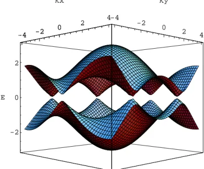
E±(kx, ky) = ±t s 1 + 4 cos √ 3kxa 2 cos kya 2 + 4 cos 2 kya 2 (1.1.8) E+(k) and E−(k) are called bonding π and antibonding π∗ energy bands. One can
see that at the corner point K in the first Brillouin zone, both bands take the same energy E = 0, therefore there is no band gap between two bands (See Fig 1.2). As there are two inequivalent atoms in the unit cell, the antibonding band π∗ will be
completely filled, the Fermi level will be at E=0. We will see below that this has a strong influence on the electronic structure of a single-wall carbon nanotube.
-4 -2 0 2 4 kx -4 -2 0 2 4 ky -2 0 2 E -4 -2 0 2
Figure 1.2: The energy dispersion relations for a two-dimensional graphene sheet are shown. The bonding and antibonding bands cross each other at K points. Therefore it is a zero gap semiconductor. The plot is in arbitrary unit.
1.2
Single-Wall Carbon Nanotube
1.2.1
Atomic Structure
A single-wall carbon nanotube can be described by rolling up a graphene sheet. The most important parameter to define the atomic structure of a SWNT is the chiral vector Ch (the vector in OA the Fig 1.3), which corresponds to the perimeter of the
nanotube. The chiral vector can be expressed by the two unit vectors a1 and a2 of
the graphene lattice in the real space:
Ch = na1+ ma2 ≡ (n, m) (1.2.1)
where n and m are integers, satisfying 0 ≤ m ≤ n (because of the hexagonal symmetry of the graphene lattice, we need to only consider the cases 0 ≤ m ≤ n). For the case n=m, this is the so-called armchair nanotube; for m=0 it is called zigzag nanotube; all other (n,m) chiral vectors correspond to a chiral nanotube.
a2 a1 O B A C x y Ch T q
Figure 1.3: The unrolled honeycomb lattice of a nanotube. OA is the chiral vector Ch, OB signifies the translation vector T, the rectangle OACB defines the unit cell of
a nanotube, θ is the chiral angle, and ai, i = (1, 2) is the unit vector of the graphene
lattice in real space.
From the chiral vector, one can easily find that the diameter dt of a nanotube is
dt= |Ch| /π = a
√
n2+ m2+ nm/π (1.2.2)
where a is the lattice constant of the graphene layer defined in the previous section. One can also define the chiral angle θ between the chiral vector Ch and a1 :
cos θ = Ch· a1 |Ch| |a1|
= 2n + m
2√n2+ m2+ nm (1.2.3)
where θ is limited by 0 ≤ |θ| ≤ 30◦because of the hexagonal symmetry of the graphene
Apart from the chiral vector Ch, one can define the translation vector T, which
is the unit vector of the nanotube. The translation vector is parallel to the nanotube axis and is normal to the chiral vector. As seen in the Fig 1.3, it corresponds to the first lattice point B of the graphene layer through which the vector passes. One can find
T= t1a1+ t2a2 ≡ (t1, t2) (1.2.4)
where t1 and t2 are integers, and they do not have a common divisor except the unity.
The precise expression for t1,2 is
t1 = 2m + n dR , t2 = − 2n + m dR (1.2.5) where dR is the greatest common divisor of (2m + n) and (2n + m).
Since both the chiral vector and the translation vector have been defined, one can therefore find the unit cell of the one-dimensional nanotube, which is the rectangle OACB in the Fig 1.3 generated by Ch and T. The number of carbon atoms in a unit
cell is given by 2N, where N is N = |Ch× T| |a1× a2| = 2(m 2 + n2+ nm) dR = 2π 2d2 t a2d R (1.2.6) Above we presented briefly the atomic structure the a SWNT in real space, we can now turn to the reciprocal space. Two reciprocal lattice vectors K1 and K2 can be
defined. K1 is in the circumferential direction and K2 is along the tube axis. Using
the definition relations below
Ch· K1 = 2π, T · K1 = 0
Ch· K2 = 0, T · K2 = 2π (1.2.7) one can find that
K1 = 1
N(−t2b1+ t1b2), K2 = 1
N(mb1− nb2) (1.2.8) As the nanotube is one-dimensional material, only K2 is a real reciprocal unit
vector for a SWNT. The length of the first Brillouin zone is given by |K2| = 2π/ |T|.
For the vector K1, it is not a reciprocal unit vector of the nanotube, however
it gives the discrete k value in the direction of Ch, with k = k K2
|K2| + µK1, −
π |T| ≤
circumferential direction of the nanotube, wavevectors in this direction become quan-tized. Since N K1 = (−t2b1+ t1b2) is a reciprocal unit vector of the graphene sheet,
two wave vectors which differ by N K1 are equivalent. Therefore, there are N
differ-ent wave-vectors µK1 that give rise to N discrete k vectors, and N one-dimensional
sub-bands of a nanotube appear.
1.2.2
Electronic Structure
The electronic structure of a SWNT can be deduced from that of a graphene layer. As we mentioned above, because of the periodic boundary condition in the circumfer-ential direction of the nanotube, the electron wave-vector in this direction becomes quantized. On the other hand, the wave-vector along the direction of tube axis re-mains continuous provided that the length of the nanotube is infinite. Therefore the energy bands of a SWNT can be obtained from cross sections of those of a graphene layer.
One may take the example of a armchair nanotube (n,n). Using the definitions above, one may find the chiral vector Ch is in the direction ex; and the translation
vector T, which is normal to the chiral vector, is in the direction ey :
Ch = n(a1+ a2) = n
√ 3aex
T= a1− a2 = aey
(1.2.9) Because of the periodic boundary condition in this direction, the electron wave-vector kx becomes quantized,
n√3kx,q = 2πq, (q = 1, 2...2n) (1.2.10)
On the other hand, the electron wave-vector ky along the tube axis, in this case
in the direction ey, remains continuous. On substituting Eq.1.2.10 into Eq.1.1.8, one
finds the following dispersion relation: E±,q(k) = ±t r 1 + 4 cosqπ n cos ka 2 + 4 cos 2 ka 2 (1.2.11) where ± denotes the bonding π and antibonding π∗ bands, q is the integer between 1
and 2n that denotes the sub-band index, and −π ≤ ka ≤ π signifies the first Brillouin zone.
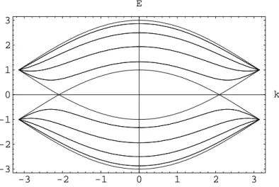
For an armchair SWNT (n,n), one can easily find, for both bonding and anti-bonding bands q=n, E(k = ±2π/3a) = 0, the anti-bonding and antianti-bonding sub-bands
cross each other. There are in total 2n antibonding sub-bands; as the number of π electrons is equal to that of the carbon atoms, which is 4n as derived from Eq 1.2.6, therefore all the antibonding sub-bands are fully occupied. The fermi level is at the crossing point. This makes the armchair SWNT a metallic nanotube. And there are four transport channels at the Fermi lever, factor 2 comes from the spin degeneration. Fig 1.4 shows the dispersion relations calculated from the above equation for an armchair SWNT (5,5). -3 -2 -1 0 1 2 3 -3 -2 -1 0 1 2 3 k E
Figure 1.4: One dimensional energy dispersion relations for an armchair SWNT (5,5). Those bands with positive energy are antibonding π∗ sub-bands and those with
neg-ative energy are bonding π sub-bands. The bonding and antibonding sub-bands with band label q=5 cross each other at k = ±2π/3a. The Fermi level is at the crossing point. The plot is in arbitrary units.
The electronic band structure of zigzag and chiral nanotubes can also be derived from that of a graphene sheet. They can be metallic or semiconducting, depending on the index of nanotube (n,m). The general condition for metallic nanotubes is that (n-m) is a multiple of 3 [22].
We at last need to mention the Peierls Instability. In general metallic 1-D ma-terials are unstable under a Peierls distortion, however it has been found that for metallic SWNT, the energy gap due to the Peierls distortion decreases rapidly to zero when increasing the diameter of the tube [23, 24]. Therefore both metallic and semiconducting SWNTs exist.
Chapter 2
Techniques of Sample Fabrication
and Characterization
We have briefed in the previous chapiter the fundamental properties of carbon nan-otubes. We are specially interested in electron transport properties of single-wall carbon nanotubes (SWNT). To probe these properties, metal electrodes need to be made to carbon nanotubes so that I-V curves can be registered. In this chapiter, we will present various techniques related to sample fabrications (Sec.2.1) and sample characterizations (Sec.2.2).
2.1
Sample Fabrication
A single-wall carbon nanotube is a several-µms long cylinder, whose diameter is usu-ally less than 2nm. Making electrical contacts to such a small object needs tens of hours work. To ensure the quality of the sample, most of the sample-fabrication work need to be carried out inside a clean room. The experimental equipments, such as beakers, flasks and tweezers, should be cleaned before the utilization and kept in a clean space. The choice on solutions used to clean equipments can be made among rectapure acetone, rectapure 2-isopropanol and deionized water, depending on the object to be cleaned. An object may be cleaned several times with different solution before the use, and the cleaning is mostly made in a ultrasonic tank (100W, 42Khz).
2.1.1
Preparation of the Silicon Wafer
To make a electrical contact to a SWNT, we need first to find an isolator to support the nanotube. We therefore use a doped silicon wafer with a 500nm thick silicon-oxide
layer on the top. We usually cut a large silicon wafer into small pieces with a typical size of 8mm×8mm. We then clean the wafer by dipping it successively in acetone, deionized water, nitride acid, deionized water again and at last 2-isopropanol. The cleaning is done in the ultrasonic tank . Each step take one minute except the first one in acetone, which takes five minuets instead. Cautions need to be taken when transferring the wafer from one solution to another. One should behaves quickly in order to not dry the wafer, if not dirties will be left on the wafer surface. The final drying process is done with a gun of azote gas (that’s why it is important to verify the pressure in the bottle of azote before cleaning the wafer). The typical roughness of the wafer surface is around one 1nm.
2.1.2
Alignment Marks
Once the silicon wafer is cleaned, nanotubes can be deposited on it. However, as nanotubes will be put onto the wafer in a random way, one would need something to help to determine the position of a nanotube. Therefore alignment marks need to be evaporated onto the wafer surface before the deposition of tubes (Indeed, alignment marks can also be fabricated after the deposition of tubes. This is another technique for contacting nanotubes grown by Chemical-Vapor -deposition method. We will not go into details here). These metallic marks are fabricated using lithography technique, which will be discussed in the subsection below. The highness of an alignment mark is often tens of nms. They can be further classified into two groups: the size of large one is several hundreds µms, that of small one is about a few µs. The combination of large and small alignment marks allows us to determine the position of a nanotube with a precision down to 50nms.
2.1.3
Deposition of Nanotubes
Now we have a silicon wafer with pre-fabricated alignment marks, we can start to deposit the carbon nanotubes onto the wafer. Carbon nanotubes fabricated by laser-ablation methods look like black powder, tubes are usually intertwisted into bundles. In order to get isolated nanotubes, the traditional method involves the use of ultra-sonic bath. which can help dispersing the nanotubes from bundles. A few pieces of carbon nanotubes are firstly put into a small bottle, inside which there is 3-5 cm3
of dichloroethane solution. The bottle is then suspended in the ultrasonic tank. We usually leave the bottle in the tank for about 45 minuets. One should know that long time, high ultrasonic intensity will induce disorder inside the nanotube.
Once the ultrasonic bath is done, one needs to begin immediately the deposition of nanotubes onto the silicon wafer because tubes in the dichloroethane solution tends to intertwist with each other as time passes. The deposition is made by a technique called spin-coating. One or two drops of the nanotube solution are put on the wafer so that at least 2/3 of wafer surface is covered. The wafer is then rotated with relatively low speed (acceleration: 1000 circle/min2, velocity: 1000 circle/min). About 5
seconds later, when the color of the wafer change (that means the solution on the surface is almost dried), we increase the velocity to 2000 circle/min. Keeping this velocity for 25 seconds, the deposition is completed. The above process need to be repeated several times in order to get a appropriate tube density on the wafer, which can be checked under the Atomic Force Microscope (AFM).
2.1.4
Locating the Carbon Nanotube
We usually locate the carbon nanotube under an Atomic Force Microscope, which can give the image of the wafer surface. The position of a nanotube is determined with respect to the four alignment marks around it (Fig 2.1). The diameter of a nanotube can also be roughly found from its highness in the AFM image with a precision down to 1nm. We can therefore select the best nanotube to contact, on considering tube itself (usually the tube need to be long, strait, with homogenous diameter along the total length of the tube), its nearby environment (too much dirties/tubes around may make the contacts bad or cause short-current.)
2.1.5
Making Electrical Contacts to Nanotubes
Once we decide the nanotube to be contacted, we can now put metal electrodes onto the selected area of the nanotube. This can be down using electronic lithography, which protected the undesired area from the metal evaporation.
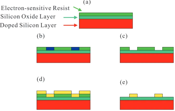
Lithography is the traditional technique for printing on a smooth surface. The essence of electronic lithography is the same as its ancestor. Fig 2.2 illustrate the different step of an electronic lithography procedure: firstly, a layer of electro-sensitive
Figure 2.1: The AFM image shows catbon nanotubes on the surface of a silicon wafer. Four alignment marks lie at the corners of the image, which serve as the references to locate a nanotube.
resist (polymer) is deposited on the top surface of the silicon wafer. The wafer is then selectively exposed to high-energy electron beam (25kev) in a controlled manner. The high energy electron breaks inter-chains of the polymer molecular, therefore degrading the resist in those exposed area. The degraded resist can be lifted through the developing process, while the left resist on the surface still covers the undesired area. The metal evaporation can now be done and electrodes are attached to the nanotube. After washing off the rest resistor in hot acetone solution (Lift-Off), the sample fabrication is completed.
Deposition of the Resist
To facilitate the Lift-Off process, we deposit successively two different electro-sensitive resist, first MAA (Methacrylic Acid solution) then PMMA (Polymethyl Methacrylate solution), onto the silicon wafer. The deposition is also done with the spin-coating method (acceleration: 4000 circle/min2, velocity: 4000 circle/min, time: 30
sec-onds). After the deposition of the MAA, the wafer need to be heated to 160 Celsius degrees for at least 5 minuets evaporate the solvent. The wafered need to be cooled for one minuet before the deposition of the PMMA, in order to not damage the latex airproof gasket. One can then deposit the PMMA, the wafer is finally reheated to
(a)
(b)
(c)
(d)
(e)
Electron-sensitive Resist
Silicon Oxide Layer
Doped Silicon Layer
Figure 2.2: (a) The electro-sensitive resist deposited on the top surface of the silicon wafer. (b)High energy electrons attack the selected area on the resist layer, cutting the interconnections between polymer chains. (c) After the development, the degraded resist is lifted. (d) Metal evaporation covers a metallic layer on the top of the wafer. (e) Lift-off process takes away the undesired metal parts.
160 Celsius degrees for more than 15 minuets to evaporate the solvent. Electronic Lithography
Electronic lithography is carried out inside a Scanning Electron Microscope (SEM, model: JEOL 2200). After the wafer is loaded into the chamber, one need first optimize different parameters of the SEM, in order to get it well focused on the wafer surface.
Then the alignment procedure to locate nanotubes must be down. This involves several steps:
1. To locate the position of the wafer by one pre-selected corner, it functions as the reference point for large structure. The x-y coordinates of the corner are read from rulers on the SEM with a precision down to 10 µms.
2. Knowing the relative positions of alignment marks with respect to the reference point, zoom the view-field into the area with the alignment marks.
3. Another alignment process is done to locate several special alignment marks serving as reference points for small structures. The position of a nanotube can therefore be determined with a precision down to 50 nms.
One can then expose the selected area of the wafer surface to electron beam. The geometry of the electrode is thus defined. Parameters like beam intensity, exposing time can be controlled by the software.
Development
We use a mixed solution of Methylisobutylcetone (MIBK) and 2-Isopropanol (IPA) to develop the exposed resist. The solution is made with one volume of MIBK and three volume of IPA. The wafer need to be washed in the solution for 70 sec-onds, then transferred to the solution of IPA for more than 30 seconds to stop the developing. The temperature of the mixed solution can dramatically change the ef-fect of the development. To our experience, 18-20 Celsius degrees is the appropriate temperature.
Evaporation
The deposition of metal electrodes is done with the metal evaporation. The metal electrode is mostly fabricated with Cr/Au in our experiments. One layer of Cr (3-5nm
thick) is first evaporated onto the wafer for that Cr can well adhere to silicon oxide. Then the second layer of Au (40-100nm thick) can be evaporated. The evaporation is done in high-vacuum (10−6mbar) by heating the material through Joule Effect. As
large quantity of gas molecules are absorbed on the surface of Cr, a degassing process is necessary before the evaporation, which can be down by slightly heating the Cr in the vacuum.
Lift-off
After the evaporation, the wafer is completed covered by a metallic layer. To lift the undesired metal layer, one need to leave the wafer in hot acetone (54 Celsius degrees) for 10 minuets. A syringe is used to eject acetone flux onto the wafer surface to help to remove the metal layer. The wafer is then cleaned in 2-isopropanol.
2.2
Sample Characterization
After the metal electrodes have been successfully attached to a nanotube, the electri-cal transport measurement can be performed under a probe-station or inside a Helium 4 cryostat.
Measurement under a Probe-Station
Under the probe-station, the nanotube device is contacted by metal tips, which can be manipulated in x-, y- and z- three directions under a binocular microscope. One need to take cautions when manipulating the metal tips. As the oxidized silicon isolation layer of the sample is only 500nm thick, the metal tip must make a stable however slight contact with the electrode in order to not penetrate the isolation layer, otherwise a short-circuit with the underground doped silicon layer will totally destroy the sample. Another caution that needs to be taken by a manipulator is the hazard of electro-static charge. The electro-static potential carried by a manipulator can be up to several thousands volts. Such a high voltage can easily induce a large pulse current through the nanotube and burn it down if a direct contact between the manipulator and the sample is constructed. Therefore the manipulator need to always keep himself discharged when doing the measurements under the probe-station. Indeed, once the metal electrodes have been attached to the nanotube, one need to take the caution
against the hazard of electro-static charge when handling the sample. Wire-bonding
We usually perform only preliminary measurements under the probe station to select some best devices for further investigations. Most of the measurements are afterward carried out inside a Helium 4 cryostat.
In order to load the sample into the cyostat, it needs to be sticked to a chip carrier using the silver lacquer. The electrical contacts between electrodes on the sample and on the chip-carrier are constructed by Au or Al thread with a 25 µm diameter. This can be down by a specific machine, which joints the metal thread with the electrode by a ultrasonic shock. This is called the wire-banding, which is one of the most delicate step in the whole experiment. One should be very patient in this step. Measurement inside a Helium 4 Cryostat
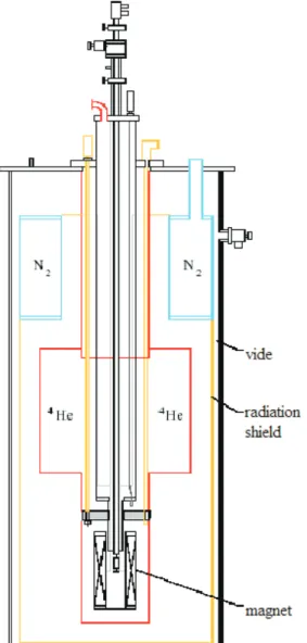
Once the wire-banding is successfully done, one can load the sample into the cryostat, which allows us to perform the measurements in a temperature region from 1.4K to 300K, with a magnetic field up to 8 Tesla. The conductance of the sample as a function of temperature or magnetic field can therefore be registered. The measured current and voltage signals are amplified and transferred to voltage signals, which are collected by the computer through a AD-DA card. The whole data collection process is controlled by a Labview programme. Below is the figure which gives a simple description to a Helium 4 cryostat.
Figure 2.3: Schematic view of a Helium 4 Cryostat. The sample is to be loaded at the lower end of the rod in the middle.
Chapter 3
Non-invasive Four-terminal
Measurements on Single Wall
Carbon Nanotubes
Transport measurements has so far proven itself as a powerful tool to investigate the electronic properties of molecular systems [25]. Most often, individual molecular systems are electrically attached to two nano-fabricated electrodes. However, such two-terminal experiments do not allow the determination of the intrinsic resistance that results from the scattering processes involving, e.g. phonons or disorder. Indeed, the resistance is mainly dominated by poorly defined contacts that lie in series. A solution to eliminate the contribution of contacts has been found with scanning probe microscopy techniques [26, 27, 28, 29, 30], which enable the measurement of resistance variations along long systems such as nanotubes, however so far these techniques have only been applied at room temperature. The standard method to determine the intrinsic resistivity of macroscopic systems is the four-terminal measurement. However, the application of this technique to molecular systems is challenging, , since the metal electrodes used so far have been invasive. For example, nano-fabricated electrodes were shown to divide nanotubes into multiple quantum dots [31, 32].
To overcome this difficulty, we have designed a new four-terminal resistance mea-surements technique on single wall carbon nanotubes(SWNTs), which employs mul-tiwalled carbon nanotubes(MWNTs) as noninvasive voltage electrodes. With this technique, we have found that SWNTs are remarkably good one-dimensional con-ductors with resistances as low as 1.5kΩ for a 95nm long section. The resistance of
nanotube is shown to linearly increase with length at room temperature, in agree-ment with Ohm’s law. At low temperature, however, the resistance can become negative and the amplitude then depends on the transmission coefficients at the dif-ferent tube-probe interfaces. In this regime, four-terminal resistance measurements can be described by the Laudauer-B¨uttiker formalism [33, 34, 1], which takes into account quantum-interference effects.
This chapiter is organized as follows. In Sec. 3.1, we give a brief review of the previous efforts to measure the intrinsic resistance of SWNTs. In Sec. 3.2, we discuss the four-terminal resistance measurement in both the non-coherent and the coherent transport regime using Laudauer-B¨uttiker formula. In Sec. 3.3 we give a simple introduction to Coulomb Blockade (CB) oscillations of conductance, as we will use CB measurements to investigate the invasiveness of MWNTs as voltage probes. In Sec. 3.4 we give the details of our device fabrication technique, which mainly consist in moving MWNTs on the silicon oxide substrate to place them onto a SWNT. In Sec. 3.5 we give the various experimental evidences showing that MWNTs are non-invasive electrodes. The four-terminal resistance as a function of the tube length measured at room temperature, and the two-terminal coulomb blockade measurements will be presented. In Sec. 3.6 we discuss the four-terminal resistance measurements carried out at liquid Helium temperature. The interesting finding of negative four-terminal resistance strongly supports the predictions of the Laudauer-B¨uttiker formalism.
3.1
How to Probe the Intrinsic Resistance of a
Sin-gle Wall Carbon Nanotubes ?
A disorder-free SWNT connected to ideal contacts is expected to display a conduc-tance equal to 4e2/h, which is called the contact resistance R
c where the factor 4
comes from band and spin degeneracy. However, most often the contact between metal electrode and SWNT is not perfect, and there might be some disorder along the tube, the measured two-terminal resistance is a sum of quantum contact resistance Rc, tube-electrode interface resistance Ri, and the intrinsic resistance of a SWNT Rin
due to static impurities, internal reflections due to tube bending effect and to phonon scattering, etc. Therefore the usual two-terminal measurements cannot give enough information to infer the actual intrinsic resistance of a SWNT.
A solution to eliminate the contribution of contacts has been found with scanning probe microscopy (SPM) techniques [26, 27, 28, 29, 30]. In these experiments, the SPMtips are used as movable electrodes, which enable the measurement of resistance variation along long systems such as nanotubes. However, these techniques have only been applied at room temperature.
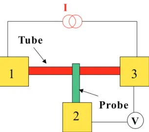
The standard method to determine the intrinsic resistivity of a macroscopic system is the four-terminal measurement. Fig.3.1 below shows the principle of the measure-ment: a voltage bias is applied across the sample, maintaining a current I through the sample. Two voltage probes are attached to middle of the sample, a voltmeter is used to measure the voltage difference between both voltage probes. As there is no net current flowing through the voltage probes, the measured resistance R = V /I does not depend on the contacts. Therefore the intrinsic resistance of the system can be obtained.
V
+-I
1
3
4
2
V
+-I
V
V
+-I
1
3
4
2
Figure 3.1: The setup of four-terminal resistance measurement: I is the current in-jected in 1 and extracted in 2 through the object, and V is the voltage difference between the two voltage probes 4 and 3. R=V/I gives the intrinsic resistance of the object.
However, the application of this technique to a SWNT is challenging, since the metal electrodes used so far have been invasive [31, 32]. The metal electrodes can damage the SWNT in two different ways.
Firstly, the metal electrodes may induce tunnel barriers into the SWNT. There are two different approaches to attach metal electrodes to a SWNT. The tube may be deposited on top of the prefabricated electrodes; or the electrodes may be evaporated on top of the tubes. In the former case, the mechanical bending within the tube may create successive quantum-dots inside the tube (as shown in Fig 3.2); in the latter case, though the origin is not very clear yet, electrodes also introduce barriers into
Figure 3.2: Mechanical bending within the tube create tunnel barriers near edges of electrodes inside the tube. The tube is divided into three quantum dots. One lies between two metal electrodes, and the other two lie on the top of electrodes.
the tube. The possible explanations are the damage by electron beam and the doping effect on the tube by metal electrodes.
Below is an example taken from Ref.[31]: Fig 3.3 shows a long SWNT deposited on prefabricated metal electrodes. At low temperature, two-terminal conductance measurements between non-adjacent electrodes give aperiodic Coulomb peaks, sug-gesting the existence of multiple quantum-dots along the measured SWNT. Further investigations suggest the location of the barriers is near the edge of the metal elec-trodes, where the barriers may be induced by bending of tube at the edge of the electrodes, as seen in Fig 3.2.
Figure 3.3: (a) AFM image showing a nanotube over prefabricated Pd electrodes. (b) Two-terminal measurements of the current versus gate voltage between various pairs of electrodes i-j at 4K. Curves are vertically offset for clarity.
Even if the electrodes cause no damage, the metal electrodes can be invasive in a more fundamental way. As seen in the Fig 3.4 below, an electron traveling in the SWNT can enter the voltage probe. As the voltage probe itself is electrically floating, no net current flows in or out of it, so another electron must come out. However, this electron can take either directions, this generates an additional resistance.
Figure 3.4: Additional back-scattering created by a voltage probe placed above a SWNT. Arrows show the incoming and outgoing electrons.
To investigate in detail this additional backscattering, we can start with the scat-tering matrix (S-matrix) related to the voltage probe. A S-matrix relates the outgoing wave amplitudes to the incoming wave amplitudes at different leads. Like the config-uration in the Fig 3.5 below, the S-matrix which describes locally the voltage probe can be written as b1 b2 b3 = a √ǫ b √ ǫ c √ǫ b √ǫ a a1 a2 a3 (3.1.1) Where bi and ai are outgoing and incoming wave fuction amplitudes of the electrode
i, respectively, and c = √1 − 2ǫ, a = (1 − c)/2, b = −(1 + c)/2, ǫ is the coupling parameter between the tube and the voltage probe [35]. Here we suppose there is no other static scattering center along the tube, and all metal electrodes make transparent contacts. The analysis below is made in the non-coherent transport regime.
The transmission probability Tnm between from m to n is obtained by the
magni-tude of the corresponding element of the S-matrix:
Tnm = |Snm|2 (3.1.2)
The transmission probability matrix can be written as a2 ǫ b2 ǫ c2 ǫ b2 ǫ a2 (3.1.3)
1
3
2
Tube
Probe
V
I
Figure 3.5: A three terminal device with which we calculate the additional resistance introduced by the probe.
Therefore the total transmission probability between tube and voltage probe Ttube−probe is 2ǫ.
Using B¨uttiker formula, Im = 4e
2
h
P
n[TnmVm− TmnVn], where Vm and Im are the
potential and the current of electrode m, respectively. We therefore have the following expression I1 I2 I3 = 4e2 h T12+ T13 −T12 −T13 −T21 T21+ T23 −T23 −T31 −T32 T31+ T32 V1 V2 V3 (3.1.4) On taking V3 as zero, and using the Kirchoff’s law (I1+ I2+ I3 = 0), we can find the
the following I-V relations: µ I1 I2 ¶ = 4e 2 h µ b2+ ǫ −ǫ −ǫ 2ǫ ¶ µ V1 V2 ¶ (3.1.5) from which we can find that the two-terminal resistance R2pt between lead 1 and 3 is
R2pt = · V1 I1 ¸ I2=0 = 1 b2 + ǫ/2 h 4e2 (3.1.6)
therefore if the transmission probability between tube and voltage probe is around 0.4, we get an additional resistance ≈ 0.1 h
4e2. In order to get rid of this additional
resistance, the transmission probability Ttube−probe between tube and voltage probe needs to be weak.
Experimentally, one can estimate the Ttube−probe by measuring the resistance be-tween the tube and voltage probe. We have
Rtube−probe =· V2 I2 ¸ I1=0 = 1 ǫ b2+ ǫ 2b2+ ǫ h 4e2 ≈ 2ǫ1 4eh2 = 1 Ttube−probe h 4e2 (3.1.7)
in the weak coupling limit.
Above we have analyzed the invasiveness of voltage probes. In order to find the intrinsic resistance of a SWNT with four-terminal measurement technique, one need to attach some non-invasive voltage probes to a SWNT. We propose to use MWNTs as voltage probes, since the electrical transmission between two crossed nanotubes is low [36, 17]. These MWNTs can be attached to the SWNT by AFM manipulations. We will see in the Sec. 3.4 the details concerning how to place a MWNT onto a SWNT with the help of the AFM tips.
3.2
Laudauer-B¨
uttiker Formalism
3.2.1
General Description of a Four-Terminal Device by the
Laudauer-B¨
uttiker Formalism
In this section we will give a brief introduction to the Laudauer-B¨uttiker formalism, which is the theory mostly employed in the description of multi-terminal electron transport in mesoscopic systems. Both non-coherent and coherent electron transport in a four-terminal system will be discussed.
The basic equation that describes the I-V relations in a multi-terminal structure is:
Im =
X
n
[GnmVm− GmnVn] (3.2.1)
where Vm and Im are the potential and the current of electrode m, respectively; and
Gnm is the conductance coefficient from the electrode m to the electrode n. We can
express Gnm with the transmission coefficient Tnm:
Gnm = 4
e2
where the factor 4 comes from the fact that there are 2 spin-degenerated transport channels at the Fermi level of a SWNT.
Therefore the I-V relations in a four-terminal device as described in the Fig 3.6 can be written as I1 I2 I3 = 4e2 h T12+ T13+ T14 −T12 −T13 −T21 T21+ T23+ T24 −T23 −T31 −T32 T31+ T32+ T34 V1 V2 V3 (3.2.3) We have taken the voltage V4 to be zero, and I1+ I4 = 0.
Probe
1
4
2
SWNT
V
I
3
Probe
1
4
2
SWNT
V
I
3
1
4
2
2
SWNT
V
I
3
3
Figure 3.6: A four-terminal measurement setup on a SWNT. The current I flowing from terminal 1 to 4. A voltage drop V is measured between the floating terminal 2 and 3.
We now take the reciprocal of the transmission matrix, then we have V1 V2 V3 = R I1 I2 I3 (3.2.4) where the resistance matrix [R] is given by
R= h 4e2 T12+ T13+ T14 −T12 −T13 −T21 T21+ T23+ T24 −T23 −T31 −T32 T31+ T32+ T34 −1 (3.2.5) The four-terminal resistance R4p measured in the configuration shown in Fig 3.6 is
given by R4p= V I = · V2− V3 I ¸ I2−I3=0 = R21− R31 (3.2.6)
3.2.2
Non-coherent Electron Transport Regime
We first treat the electron motion classically, therefore we do not worry about any interference effect. We will take a simple model shown in the Fig 3.7. This is a SWNT contacted by four electrodes, among which electrodes 1 and 4 are current probes, electrodes 2 and 3 are voltage probes. Supposing there are three static scatters along
Probe
1
4
2
SWNT
V
I
3
T
leftT
middleT
rightProbe
1
4
2
2
SWNT
V
I
3
3
T
leftT
middleT
rightFigure 3.7: A four-terminal measurement setup on a SWNT, along which lie three static scatterers. One to the left of electrode 2 is called Tlef t, where Tlef talso signifies
its transmission probability. Tright and Tmiddle are defined in the same way.
the tube, each can be characterized by a (2 × 2) scattering matrix µ i√√1 − Ti √Ti
Ti i√1 − Ti
(3.2.7) where Ti is the transmission probability of the static scattering center i.
The effect of voltage probes, as we have seen in the first section, can be described by a (3 × 3) scattering matrix a √ǫ b √ ǫ c √ǫ b √ǫ a (3.2.8) where c =√1 − 2ǫ, a = (1−c)/2, b = −(1+c)/2, ǫ is the coupling parameter between the tube and the voltage probe.
These scattering matrix relate the outgoing electron wave amplitudes to the in-coming electron wave amplitudes. What we need to do now is to combine all these
scattering matrix together to find the total transmission matrix. Because we are in non-coherent transport regime, we may neglect the phase factor of the electron wave. Instead of combining successive scattering matrix, we can combine directly the probability matrix to get the total transmission matrix. The probability matrix is obtained by taking the squared magnitude of the corresponding element of the scat-tering matrix, therefore we have the following probability matrix related to the static scattering center
µ 1 − Ti Ti
Ti 1 − Ti
(3.2.9) and to the voltage probe
a2 ǫ b2 ǫ c2 ǫ b2 ǫ a2 (3.2.10) The method to combine different probability matrix into a composite matrix is described in [1]. We give in the appendix the Mathematica programme for details of the calculation. We present here the main results of the calculation.
1. The calculated four-terminal resistance R4p does not depend on the
trans-mission probabilities Tlef t and Tright as shown in the Fig 3.8 below. The similar
dependence on Tlef t can also be obtained.
0.2 0.4 0.6 0.8 1 T-right 0.25 0.5 0.75 1 1.25 1.5 1.75 2 R4p
Figure 3.8: Four-terminal resistance R4p as a function of the transmission Tright, with
Tlef t=0.1, Tmiddle = 0.5, ǫ1,2 = 0.01, the R4p is in unit of 4eh2.
2. The calculated four-terminal resistance R4p does depend on the coupling ǫ1,2
between voltage probes and the SWNT, as seen in Fig 3.9. The four-terminal re-sistance increases with the coupling strength ǫ, as we have seen in the first section,
this is due to the additional backscattering caused by the voltage probes. For weak coupling between the voltage probe and the SWNT, R4p tends to 4eh21−Tmiddle
Tmiddle , which
is the intrinsic resistance of the SWNT as we will see below.
0.1 0.2 0.3 0.4 0.5 e1 1.1 1.2 1.3 1.4 1.5 R4p
Figure 3.9: Four-terminal resistance R4p as a function of the the coupling strength
ǫ1, with Tlef t= Tright = 0.1, Tmiddle=0.5, ǫ2 = 0.01, the R4p is in unit of 4eh2.
3. In case that the coupling between the voltage probes and the SWNT is weak, the four-terminal resistance R4pis only a function of T2. This means that R4pdescribes
only the intrinsic resistance between the two voltage probes. Indeed, the above curve
0.2 0.4 0.6 0.8 1 T-middle 1 2 3 4 5 R4p
Figure 3.10: Four-terminal resistance R4p as a function of the transmission Tmiddle,
with Tlef t=0.1, Tright= 0.1, ǫ1,2 = 0.01, the R4p is in unit of 4eh2.
takes a form of (1 − Tmiddle)/Tmiddle, as seen in Fig 3.10. We can understand this
Supposing there are several static scattering center lying in series along the SWNT between the two voltage probes. The measured four-terminal resistance should be the sum of the resistance related to each scatterer. We start by a simple case: two scatter-ers with transmission probability T1 and T2 are located inside the SWNT. To obtain
the total transmission probability T12 we need to take into account all the multiple
reflections of electron between both scatterers. As we neglect the interference, the total transmission probability is:
T12 = T1T2+ T1T2R1R2+ T1T2R21R22+ ...
= T1T2 1 − R1R2
(3.2.11) with R1,2 = 1 − T1,2 is the reflection probability of both scatterers.
We can rewrite the above result in the following form: 1 − T12 T12 = 1 − T1 T1 +1 − T2 T2 (3.2.12) The fact that the quantity (1 − Ti)/Ti has an additive property suggests that the
resistance of an individual scatterers is proportional to it. Therefore, if there are N scatterers lying along the SWNT, each has a transmission probability T, the total resistance of these scatterers should proportional to (1 − T (N))/T (N), where T (N) is the total transmission probability satisfying
1 − T (N) T (N ) = N
1 − T
T (3.2.13) This explains the above calculated four-terminal resistance R4p taking a form of 1−TT .
We can further relate the four-terminal resistance to the elastic mean-free path of electron in a SWNT. Rewrite T (N ) in the following expression:
T (N ) = T
N (1 − T ) + T (3.2.14) Provided the separation between two voltage probes is L, and ρ is the mean linear density of the scatterers, we can define the elastic mean-free path of electron in SWNT le≡ ρ(1−T )T , the total transmission T (N ) can be written as
T (L) = le L + le (3.2.15) We can find R4pt = h 4e2 1 − T T = h 4e2 L le (3.2.16) The four-terminal resistance in non-coherent transport regime can therefore provide direct information about the elastic mean-free path of electron in a SWNT.
d
1d
3d
5d
4d
2 T 1 T2S
D
MWNT MWNT I Vd
1d
3d
5d
4d
2 T 1 T2S
D
MWNT MWNTd
1d
3d
5d
4d
2 T 1 T2S
D
MWNT MWNT I VFigure 3.11: (a) The four-terminal resistance measurement on a SWNT inside which there is two static scattering center. (b) The calculated resistance ratio R4pt/R2pt as
a function of the wave vector k of the electron wave inside the SWNT.
3.2.3
Coherent transport regime
Above we discussed the four-terminal measurement in the non-coherent transport regime. This is valid for high temperature measurements where the electron-phonon interaction strongly decreases the phase coherence length of electrons. When decreas-ing the temperature, the phase coherence length increases. At low temperature, the phase coherence length of electron may become close to even longer than the sam-ple size [37, 38]. In this case, one cannot neglect the interference effects of electron waves. Therefore, to calculate the total transmission matrix, one needs to combine the successive scattering matrix coherently.
We will take a very simple model to get some intuition. We suppose that there are two static scatterers lying in the SWNT, as seen in Fig 3.11. The electron wave will also be scattered by both voltage probes. The related scattering matrix are the same as in Eq.3.2.7 and Eq.3.2.8. We also suppose that the electron propagate freely between scatterers. Therefore it will acquire a phase factor eikl after traveling
a distance l. The method to combine the scattering matrix coherently is also given in Ref [1]. We give in the appendix the complete Mathematica programme for the detailed calculation. The numerical simulations below show clearly the modulations of R4pt/R2pt as a function of wave vector k. We find the very interesting phenomenon
that the four-terminal resistance can be negative. This can be understood in the following way.
We go back to B¨uttiker formula, Ip = 4 e h X q [Tqpµp− Tpqµq] (3.2.17)
where µq is electro-chemical potential of the electrode q. From this formula, one can
easily find the resistance ratio R4pt/R2pt given by
R4pt R2pt = µ3− µ4 µ1− µ2 = T13T24− T23T14 (T13+ T23+ T43)(T14+ T24+ T34) − T43T34 (3.2.18) As we are in coherent transport regime, the incident and reflected electron waves interfere with each other. Therefore, when varying the electron wave vector k, we get different interference pattern, which enable the sign reversal of the numerator in Eq.3.2.18.
3.3
Introduction to Coulomb Blockade Oscillations
of Conductance
As we will use Coulomb Blockade (CB) measurements to determine the invasiveness of MWNTs as voltage probes, we give a simple introduction to CB in this section to get some intuition.
Coulomb Blockade oscillations of the conductance are the manifestation of single electron tunneling through a quantum dot. The conductance oscillates as the voltage Vg of a nearby gate electrode is varied. We now seek to understand the origin of this
conductance oscillation phenomena.
The Fig 3.12 below is simple model of of a quantum dot contacted to the external electron reservoir through tunnel junctions. The linear response conductance of a quantum dot is defined as G ≡ I/V , in the limit V → 0. At low temperature, the electron tunneling is usually blocked. This is due to the large charging energy of the quantum dot. The capacitance C of a quantum dot is small, therefore putting an additional electron into a quantum dot will cost a significant of energy (in the order of e2/C), the energy. However, in certain situation, adding an electron into the dot
C
gateC
dot/2
Gate
Dot
Reservoir
Reservoir
C
gateC
dot/2
Gate
Dot
Reservoir
Reservoir
Figure 3.12: A schematic view of a quantum dot contacted to the external electron reservoir through tunnel junctions. The capacitance C of the dot is defined as C = Cgate+ Cdot. Because the size of the dot is very small, the charging energy of the dot
Ec = e2/C is rather large, the electron can be only added one by one into the dot.
At equilibrium, the probability P (N ) to find N electron in the quantum dot is given by the following expression [39]:
P (N ) = constance × exp(− 1
kBT[F (N ) − NE
F]) (3.3.1)
where N is the number of electrons in the dot, F(N) is the free energy of the dot, and EF is the Fermi energy of the electron reservoir measured of the bottom of the
conduction band. At zero temperature, P(N) is non-zero only for a single value, which is the integer that minimize the thermodynamic potential Ω(N ) ≡ [F (N) − NEF]. In
order to get a non-zero linear response conductance, P(N) and P(N+1) must be both non-zero, so that a very small voltage can induce a current through the dot. In order that both P(N) and P(N+1) are non-zero, that means both N and N+1 minimize the thermodynamic potential Ω, the necessary condition is Ω(N + 1) = Ω(N ), which gives
F (N + 1) − F (N) = EF (3.3.2)
At zero temperature, the free energy of the dot can be written as F (N ) ≡ U(N) +
N
X
p=1
Ep (3.3.3)
where U(N) is the charging energy, and Ep is the single electron energy level in the