POLYTECHNIQUE MONTRÉAL
affiliée à l’Université de Montréal
Contributions to modeling, simulation, and analysis of three-phase dual active
bridge converters for dc-grid integration
MAXIME BERGER Département de génie électrique
Thèse présentée en vue de l’obtention du diplôme de Philosophiæ Doctor
Génie électrique Août 2019
affiliée à l’Université de Montréal
Cette thèse intitulée :
Contributions to modeling, simulation, and analysis of three-phase dual active
bridge converters for dc-grid integration
présentée par MAXIME BERGER
en vue de l’obtention du diplôme de Philosophiæ Doctor
a été dûment acceptée par le jury d’examen constitué de :
Houshang KARIMI, président
Ilhan KOCAR, membre et directeur de recherche
Jean MAHSEREDJIAN, membre et codirecteur de recherche
Handy FORTIN-BLANCHETTE, membre et codirecteur de recherche Keyhan SHESHYEKANI, membre
ACKNOWLEDGEMENTS
First, I would like to thank M. Jacques Belley from Bombardier Transportation who believed in me twice for supporting both my master and my PhD projects. I will never forget the two amazing opportunities he gave me.
I would also like to thank M. Carl Lavertu from Bombardier Transportation for all his help during this adventure. He became more than a mentor for me, he became a friend. He cared for my success and gave many of his own personal time to help me. I consider myself privileged to learn from someone as knowledgable and as human as him every day.
I will always be grateful to my advisor Prof. Ilhan Kocar who supported me in many ways during my PhD. Ilhan gave me the opportunity to experience teaching twice and provided me support to travel and network with others. He has been very supportive, available and provided me all the guidance and advice I needed to realize my PhD project and develop my teaching skills.
Also, many thanks to Prof. Handy Fortin-Blanchette from École de technologie supérieure (ÉTS) who accepted to support me and trusted my determination to realize my project when I approached him at the end of his class. From many meetings in his office to late phone calls, he supported me all along the way. I like joking by saying that I would probably still be trying to program my FPGA modulator if it wasn’t of Handy’s advice to read Chapter 5 of the Pong P. Chu book.
Moreover, I can’t pass over the collaboration with Prof. Jean Mahseredjian. He gave me the opportunity to enter the EMTP family during my master and I consider myself very fortunate of still being a part of this family 5 years later.
I would also like to thank my lover Brigitte for all her encouragement during the best and harder moments. She was and still is my best confidant and my best friend.
Despite the distance, I will always be grateful to my parents for their unconditional support that allows me to chase my dreams. They are an important part of what I became.
A special thanks also to Mme Isabelle Provost, M. Stéphane Goulet and M. Jean-Pierre Magalhaes Grave from Bombardier Transportation for all their help and support in different ways.
Finally, this project has been financially supported by Bombardier Transportation, FRQNT, CRSNG and the Trottier Institute for Sustainability in Engineering and Design.
RÉSUMÉ
Le convertisseur cc-cc bidirectionnel isolé triphasé à deux ponts actifs (3p-DAB) est largement étudié pour son utilisation dans les réseaux à courant continu de nouvelle génération. Son intégration nécessite une modélisation précise de ses caractéristiques petit et grand signal. De plus, sa caractérisation précise en mode dégradé d’opération est un sujet important pour le développement de réseaux fiables et résilients. L’application de stratégies de modélisation bien connues au convertisseur 3p-DAB, tant en fonctionnement normal que dégradé, n’est pas triviale du fait de sa structure cc-ca-cc, des différentes connexions possibles de transformateurs triphasés et du nombre plus élevé d’interrupteurs par rapport à d’autres topologies connues. L’absence de modèles petits signaux précis ainsi que de modèles grands signaux numériquement efficace du 3p-DAB est la principale motivation des développements présentés dans cette thèse. Trois contributions principales se dégagent de ce travail.
Cette thèse contribue d’abord à l’identification des limites de l’approche conventionnelle de moyennage en espace d’état (SSA) pour la détermination des impédances d’entrée ZD et ZN du convertisseur 3p-DAB. Ces deux fonctions de transfert sont nécessaires à l’application du théorème d’éléments supplémentaires (EET) de Middlebrook qui est largement utilisé par les concepteurs en électronique de puissance pour prévenir la dégradation des performances dynamiques ainsi que les conditions d’instabilité lors de l’ajout d’un filtre d’entrée. La détermination précise de ZD et ZN est
également importante pour déduire les caractéristiques petit signal en boucle fermée du convertisseur à partir de son modèle en boucle ouverte. Bien qu’il soit démontré que l’approche généralisée de moyennage en espace d’état (GSSA) peut être utilisée pour surmonter les limites de la méthode SSA pour l’évaluation de ZD, un nouveau modèle hybride combinant SSA et GSSA est proposé pour le calcul de ZN.
La deuxième contribution de cette thèse est le développement d’un modèle moyenné généralisé (GAM) précis et efficace permettant la simulation de réseaux utilisant des convertisseurs 3p-DAB dans des logiciels d’analyses de transitoires électromagnétiques. Le modèle proposé est comparé en détail à d’autres techniques de modélisation, soit le modèle idéal en commutation, la technique des fonctions de commutation (SWF) et l’approche de moyennage en espace d’état (SSA). En somme, il est conclu que le modèle GAM fournit une solution optimale lorsqu’on
prend en compte la précision de la réponse transitoire, la réduction du temps de calcul et la largeur de bande de la réponse fréquentielle. Finalement, un réseau de simulation à grande échelle est développé dans le logiciel Electromagnetic Transient Program (EMTP) pour valider les performances du modèle GAM pour l’analyse du courant de défaut et de la tension de transitoire de rétablissement dans un système grande échelle.
La troisième contribution de cette thèse est la proposition et la caractérisation d’un nouveau mode dégradé pour le convertisseur 3p-DAB. Des travaux antérieurs ont montré que le 3p-DAB peut être utilisé dans un mode de défaillance de panne dit à phase gelée, c’est-à-dire lorsque les deux transistors d’une même phase sont forcés à l’état ouvert par les protections internes de leurs pilotes de grille. Puisque les diodes de roue libre sont laissées en autocommutation, la caractérisation analytique du convertisseur pour toutes les conditions de tension et de charge n’est pas triviale. Dans cette thèse, il est proposé d'ouvrir la phase en défaut de manière à éliminer l’interaction des diodes de roue libre au niveau de la phase défectueuse. En éliminant l’interaction de ces diodes, le 3p-DAB peut être opéré dans un mode de fonctionnement caractérisable pour toutes les conditions de tension et de charge. De plus, en raison de la circulation de courant réactif dans la phase défectueuse en fonctionnement à phase gelée, il est démontré que les contraintes de courant sont plus élevées et que la capacité de transfert de puissance du convertisseur est réduite par rapport au fonctionnement à phase ouverte proposé dans cette thèse.
ABSTRACT
The three-phase dual active bridge (3p-DAB) isolated-bidirectional dc-dc converter (IBDC) is widely investigated in next-generation dc-grids. Its successful integration requires an accurate representation of its small- and large-signal characteristics. Furthermore, accurate characterization of converters behavior in degraded-mode is an important topic for the development of reliable and resilient dc-grids. The application of well-known modeling strategies to 3p-DAB converters in both normal and degraded operations is not trivial due to its dc-ac-dc structure, the different possible three-phase transformer connections and the higher number of switches compared to other well-known IBDC topologies. The absence of accurate small-signal models as well as computational efficient large-signal models of the 3p-DAB has motivated the developments presented in this thesis. Three main contributions are emerging from this work.
This thesis first contributes to the identification of the limitations of the basic state-space averaging (SSA) approach for the determination of the driving point ZD and null driving point ZN
input impedances for 3p-DAB converters. These two transfer functions are necessary for the application of Middlebrook’s extra element theorem (EET) which is broadly used by practicing power electronic designers to avoid dynamic performance degradation or instability conditions in the presence of an additional input filter. The accurate determination of ZD and ZN is also important to derive the closed-loop small-signal characteristics of converters from its open-loop characteristics. While it is shown that the generalized state-space averaging (GSSA) approach can be used to overcome SSA limitations to evaluate ZD, a new hybrid SSA and GSSA multi-input
multi-output (MIMO) model, which combines SSA and GSSA, is proposed to evaluate ZN.
The second contribution of this thesis is the development of an accurate and computational efficient generalized average model (GAM) which enables system-level simulation of dc-grids with 3p-DAB converters in electromagnetic transient type (EMT-type) programs. The proposed model is rigorously compared with alternative modeling techniques: ideal-model, switching-function (SWF) and state-space averaging (SSA). It is concluded that the GAM model provides an optimal solution when accuracy of transient response, reduction in computation time, and wideband response factors are considered. A large-scale test system is implemented in
Electromagnetic Transient Program (EMTP) to validate the performance of the GAM model for fault current and transient recovery voltage analysis in a practical size system.
The third contribution of this thesis is the proposal and the characterization of a new degraded mode for the 3p-DAB converter. Previous work has shown that the 3p-DAB can be operated in a frozen leg fault-tolerant mode, i.e. with the two transistors of the same phase being opened by their gate driver internal protections. Because the free-wheeling diodes are left self-commutated, the analytical characterization of the converter for all voltage and loading conditions is not trivial. In this thesis, it is proposed to open the faulty-phase such as it eliminates the interaction with the faulty-phase free-wheeling diodes. By removing the interaction of the free-wheeling diodes, the 3p-DAB falls in a characterizable operating mode for all voltage and loading conditions. Furthermore, because of the circulation of reactive current in the faulty-phase in frozen leg operation, it is demonstrated that the current stress is higher, and the power transfer capability is reduced over the proposed open-phase operation.
TABLE OF CONTENTS
ACKNOWLEDGEMENTS ... III RÉSUMÉ ... IV ABSTRACT ... VI TABLE OF CONTENTS ... VIII LIST OF TABLES ...XII LIST OF FIGURES ... XIII LIST OF SYMBOLS AND ABBREVIATIONS... XVII LIST OF APPENDICES ... XIX
CHAPTER 1 INTRODUCTION ... 1
1.1 Motivation ... 1
1.2 The three-phase dual active bridge (3p-DAB) ... 4
1.2.1 Control of the 3p-DAB ... 4
1.2.2 Variants of the 3p-DAB topology ... 5
1.3 Contributions ... 7
1.4 Methodology and limits ... 12
1.4.1 Methodology ... 12
1.4.2 Limits ... 13
1.5 Thesis outlines ... 14
CHAPTER 2 STEADY-STATE ANALYSIS... 15
2.1 First harmonic approximation (FHA) in phasor-domain ... 15
2.1.1 Motivation ... 15
2.1.2 Model development ... 16
2.1.4 Application to the experimental prototype (model 4) ... 22
2.2 Piecewise-linear modeling (PLM) in time-domain ... 25
2.2.1 Motivation ... 25
2.2.2 Piecewise-linear current equations ... 25
2.2.3 Power transfer relationships ... 28
2.2.4 Zero-voltage switching (ZVS) boundaries ... 30
2.2.5 Capacitor ripple current and voltage ... 31
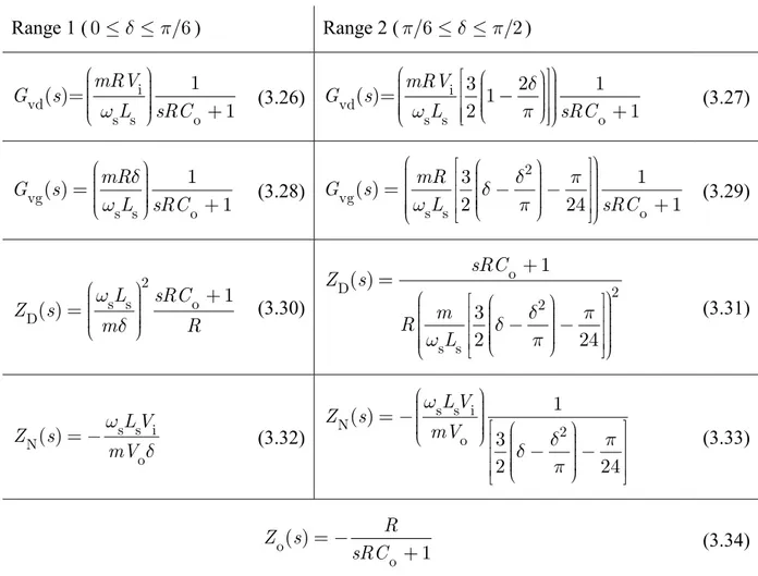
CHAPTER 3 SMALL-SIGNAL FREQUENCY-DOMAIN ANALYSIS ... 35
3.1 Small-signal model of the 3p-DAB ... 35
3.2 State-space averaging (SSA) ... 36
3.2.1 Model development ... 36
3.2.2 Derivation of the converter transfer functions ... 39
3.3 Generalized state-space averaging (GSSA) ... 42
3.3.1 Model development ... 42
3.4 Hybrid averaging and transfer functions evaluation ... 52
3.5 EMTP validation of the SSA, GSSA, and hybrid models ... 54
3.5.1 General procedure ... 54
3.5.2 Comparison of SSA, GSSA, and hybrid models ... 57
3.6 Controller sizing and closed-loop operation ... 57
3.6.1 Simplified closed-loop model for parameter sensitivity analysis with SSA ... 57
3.6.2 Complete closed-loop analysis for controller sizing ... 60
3.6.3 Closed-loop transfer functions ... 62
3.7 Input filter sizing ... 64
3.7.2 Modified transfer functions and stability analysis ... 65
3.7.3 Experimental results ... 69
CHAPTER 4 LARGE-SIGNAL TIME-DOMAIN SIMULATION ... 71
4.1 Switching-function (SWF) model ... 71
4.2 State-space averaging (SSA) model ... 72
4.3 Generalized averaging model (GAM) ... 74
4.4 Performance comparison ... 77
4.4.1 Closed-loop time-domain transient response ... 77
4.4.2 Simulation timing analysis ... 79
4.4.3 Transient short-circuit with multiple 3p-DAB ... 80
4.4.4 Closed-loop frequency-domain response ... 82
4.4.5 Transient analysis with a large-scale test system ... 84
4.4.6 Performance comparison ... 87
CHAPTER 5 OPEN-PHASE FAULT-TOLERANT OPERATION ... 90
5.1 Open-phase operation ... 90
5.2 Steady-state analysis ... 92
5.2.1 Transformer voltage and current waveforms ... 92
5.2.2 Power transfer relationship ... 96
5.2.3 Current stress in the faulty-bridge ... 98
5.2.4 ZVS soft-switching regions ... 100
5.3 Small-signal analysis ... 103
5.3.1 State-space averaging (SSA) model in open-phase ... 103
5.3.2 Generalized state-space averaging (GSSA) model in open-phase ... 107
5.4 Closed-loop transient analysis in open-phase ... 115
CHAPTER 6 CONCLUSIONS AND RECOMMENDATIONS... 121
6.1 Summary of this thesis ... 121
6.2 Future work ... 124
6.2.1 Improvements to the developed small- and large-signal models ... 124
6.2.2 Diagnosis of switch failure for post-fault open-phase operation ... 126
BIBLIOGRAPHY ... 127
LIST OF TABLES
Table 3.1: Transfer functions of the Y-Δ 3p-DAB converter obtained with SSA ... 41
Table 3.2: Closed-loop dynamic response analysis with SSA ... 59
Table 3.3: Input filter parameters ... 67
Table 4.1: Large-signal models comparison summary ... 88
Table 4.2: Summary of 3p-DAB models’ implementation in EMTP ... 88
LIST OF FIGURES
Figure 1.1 : Classification of isolated-bidirectional dc-dc converters (adapted from [11]) ... 1
Figure 1.2 : DAB topology for dc-grids interface ... 2
Figure 1.3 : Three-phase dual active bridge (3p-DAB) converter ... 2
Figure 1.4 : Control of the Y-∆ 3p-DAB converter under investigation ... 5
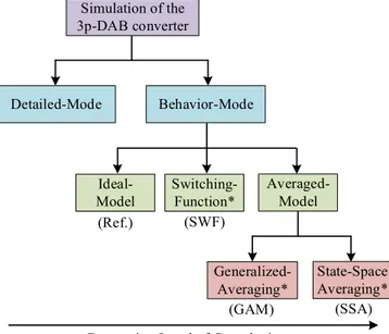
Figure 1.5 : Classification of approaches for time-domain simulation of the 3p-DAB ... 9
Figure 1.6 : Comparison of the fault-tolerant modes of the 3p-DAB ... 11
Figure 2.1 : Comparison of PLM and FHA waveforms for the Y-Δ transformer ... 16
Figure 2.2 : FHA model in physical quantities ... 16
Figure 2.3 : Typical waveforms with ZVS in the input bridge (Y-Δ transformer) ... 19
Figure 2.4 : Equivalent phasor diagrams ... 20
Figure 2.5 : Validation of the FHA design diagram for the Y-Y and ∆-∆ transformers ... 21
Figure 2.6 : Validation of the FHA design diagram for the Y-∆ transformer ... 21
Figure 2.7 : Application of FHA to the Y-∆ 3p-DAB prototype (model 4) ... 24
Figure 2.8 : Equivalent circuits for the application of PLM to the Y-∆ 3p-DAB ... 25
Figure 2.9 : Simplified representation of the Y-∆ 3p-DAB ... 27
Figure 2.10 : Waveforms for the calculation of the average output current ... 28
Figure 2.11 : Power transfer curves for the Y-∆ 3p-DAB prototype (model 4) ... 29
Figure 2.12 : ZVS regions for the Y-∆ 3p-DAB with the prototype (model 4) testing zone ... 31
Figure 2.13 : Calculation of the output voltage and current ripples ... 32
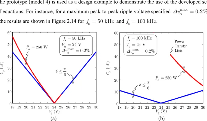
Figure 2.14 : Sizing of the output capacitor for the Y-∆ 3p-DAB prototype (model 4) ... 34
Figure 3.1 : Output voltage regulation small-signal block diagram (forward operation) ... 35
Figure 3.2 : Equivalent SSA small-signal circuits of the Y-Δ 3p-DAB converter ... 40
Figure 3.4 : Hybrid MIMO small-signal model representation of the 3p-DAB in open-loop ... 53
Figure 3.5 : Equivalent circuits for the validation of the open-loop transfer functions ... 55
Figure 3.6 : Validation of the transfer functions with time-domain simulations (model 1) ... 56
Figure 3.7 : Simplified closed-loop diagram for parameters sensitivity analysis with SSA ... 58
Figure 3.8 : Response to a step in the reference voltage from 12 V to 24 V (model 4) ... 60
Figure 3.9 : Complete closed-loop diagram for controller sizing ... 60
Figure 3.10 : Bode diagram for the sizing of the prototype controller (model 4) ... 61
Figure 3.11 : Bode diagram of the prototype controller (model 4) ... 61
Figure 3.12 : Transient response to a step in the reference voltage (prototype) ... 62
Figure 3.13 : Open-loop vs closed-loop transfer functions (model 4) ... 63
Figure 3.14 : Converter with input filter ... 65
Figure 3.15 : Input filter transfer functions magnitude ... 67
Figure 3.16 : Transient response after introduction of filters (model 4) ... 68
Figure 3.17 : Response to a step in the reference voltage from 0 V to 24 V (model 4) ... 68
Figure 3.18 : Unstable condition due to an additional input filter ... 69
Figure 3.19 : Input filter transfer functions magnitude (model 4) ... 69
Figure 3.20 : Response to a step in the reference voltage without input filter (prototype) ... 70
Figure 3.21 : Response to a step in the reference voltage with Filter D (prototype) ... 70
Figure 4.1 : SWF model of the Y-Δ 3p-DAB ... 72
Figure 4.2 : SSA model of the Y-Δ 3p-DAB ... 73
Figure 4.3 : GAM model of the Y-Δ 3p-DAB ... 74
Figure 4.4 : Simulation results for the validation of the large-signal models ... 78
Figure 4.5 : Computation time for different integration time-steps ... 79
Figure 4.7 : Simulation results for a short-circuit at the output of ten (10) 3p-DAB in parallel. ... 81
Figure 4.8 : CPU calculation effort in % of the total computation time ... 81
Figure 4.9 : Analysis of the effect of Do in fault analysis ... 82
Figure 4.10 : Equivalent circuits for the validation of the closed-loop frequency characteristics . 83 Figure 4.11 : Closed-loop frequency response ... 84
Figure 4.12 : Large-scale test system for the validation of the GAM model ... 85
Figure 4.13 : Analysis of the fault current at fault application and during fault clearing ... 86
Figure 4.14 : Analysis of the voltage V5 during fault application and fault clearing ... 86
Figure 5.1 : Protection scheme concept for frozen-leg operation (e.g. Fault on Q5, phase C) ... 91
Figure 5.2 : Protection scheme concept for open-phase operation (e.g. Fault on Q5, phase C) .... 91
Figure 5.3 : Reverse drain-source characteristic of the EPC2022 GaN FET (100V, 90A) [89] .... 92
Figure 5.4 : Simplified representation of the Y-Δ 3p-DAB with phase C open ... 94
Figure 5.5 : Theoretical waveforms for phase A (normal vs open-phase) ... 94
Figure 5.6 : Experimental waveforms for phase A in normal operation (prototype) ... 95
Figure 5.7 : Experimental waveforms for phase A in open-phase operation (prototype) ... 95
Figure 5.8 : Comparison of the power transfer capabilities (model 4/prototype) ... 98
Figure 5.9 : RMS current for different voltage and loading conditions (model 4/prototype) ... 99
Figure 5.10 : ZVS regions (normal vs open-phase) ... 101
Figure 5.11 : ZVS regions for all phases in open-phase ... 102
Figure 5.12 : Output power versus the control phase-shift with d as a parameter ... 102
Figure 5.13 : Equivalent SSA small-signal circuits in open-phase operation ... 104
Figure 5.14 : Impact of open-phase on the control-to-output transfer function (model 4) ... 112
Figure 5.15 : Impact of open-phase on the control phase-shift (model 4) ... 112
Figure 5.17 : Impact of open-phase on the input impedance (model 4) ... 115
Figure 5.18 : Closed-loop small-signal characteristics in open-phase (model 4) ... 116
Figure 5.19 : Closed-loop response for the normal operation case (prototype) ... 117
Figure 5.20 : Closed-loop response for the open-phase operation case (prototype) ... 117
Figure 5.21 : Simulation results for the transitions between the operating modes (model 4) ... 118
Figure 5.22 : Transition from normal to frozen leg (prototype) ... 119
Figure 5.23 : Transition from frozen leg to open-phase (prototype) ... 119
LIST OF SYMBOLS AND ABBREVIATIONS
1p-DAB Single-phase dual active bridge 3p-DAB Three-phase dual active bridge AC Alternating current
ADC Analog-to-digital converter CPL Constant power load CPU Central processing unit DAB Dual active bridge
DC Direct current
DPS Dual-phase-shift EET Extra element theorem
EMC Electromagnetic compatibility EMT Electromagnetic transient
EMTP Electromagnetic transient program EPS Extended-phase-shift
ESR Equivalent series resistance
FD Fault-diagnosis
FET Field effect transistor FFT Fast Fourier transform
FHA First harmonic approximation FPGA Field programmable gate array FT Fault-tolerant
GaN Gallium nitride
GSSA Generalized state-space averaging IBDC Isolated-bidirectional dc-dc converter KVL Kirchhoff’s voltage law
MANA Modified-augmented-nodal analysis MIMO Multi-input multi-output
MOV Metal oxide varistor
OS Overshoot
PI Proportional integral PLM Piecewise-linear modeling RAM Random access memory RMS Root mean square SiC Silicon carbide SPS Single-phase-shift SSA State-space averaging SST Solid-state transformer SWF Switching-function TAB Triple active bridge TPS Triple-phase-shift
UPS Uninterruptible power supply ZVS Zero-voltage switching
LIST OF APPENDICES
Appendix A – Converter model parameters ... 134
Appendix B – Small-scale prototype ... 135
Appendix C – Piecewise-linear model in normal operation ... 140
Appendix D – Complement to the SSA model in normal operation ... 152
Appendix E – Complement to the GSSA model in normal operation ... 154
CHAPTER 1
INTRODUCTION
1.1 Motivation
There is a surge of interest in academic and industrial research on dc-grids mainly due to their well-known advantages over ac-grids in several applications [1], [2]. DC distributions are being developed for applications such as transportation [3], [4], commercial and industrial buildings [5], [6], data centers [7], generating stations [8], and integration of distributed resources [9]. Power electronic interfaces play a key role in dc-grids [10], their primary functions being power flow control, galvanic isolation and voltage conversion between different grid voltage levels. Isolated-bidirectional dc-dc converters (IBDCs) are highly investigated for these applications because their structures naturally meet these three functions. IBDC topologies are classified into seven (7) categories depending on the number of switches that constitutes their switching stage (Figure 1.1).
Number of switches
Two (2) Three (3) Four (4) Five (5) Six (6) Eight (8) Twelve (12) dual-flyback, dual-Cuk Zeta-Sepic forward-flyback dual-push-pull push-pull-forward, push-pull-flyback dual-half-bridge
full-bridge-forward half-full-bridge single-phase-dual-
active-bridge three-phase- dual-active-bridge Figure 1.1 : Classification of isolated-bidirectional dc-dc converters (adapted from [11]) Among these topologies, dual active bridge (DAB) isolated bidirectional dc-dc converters (Figure 1.2) are broadly considered due to their high flexibility, and their high efficiency owing to their inherent zero-voltage switching (ZVS) capabilities [12], [13]. DAB converters are proposed to be employed in many recent conversion applications such as distributed resources interface [14], uninterruptible power supply (UPS) systems [15], automotive [16], [17], passenger rail transportation [18], solid-state transformers (SST) [19], airborne wind turbines [20], and flexible load emulators [21].
Both single-phase (1p-DAB) and three-phase (3p-DAB) versions have been proposed and protected by a patent in the early 1990s [22]. These two topologies are now public domain and are gaining a broad interest especially with the introduction of emerging semiconductor technologies which tends to reduce the negative effects of having more switches when compared to other IBDC topologies. Regardless of the higher number of switches, the 3p-DAB (Figure 1.3) provides many
advantages over the 1p-DAB which is why it tends to be favored in many modern flexible dc-grids [23]. Due to its three-phase structure, the ripple frequency is increased, thus reducing the sizing of the filter capacitors. It also reduces the current through the switches and provides a better utilization of the transformer copper and core materials.
Figure 1.2 : DAB topology for dc-grids interface
Figure 1.3 : Three-phase dual active bridge (3p-DAB) converter
The integration of power electronic converters in dc-grids brings many challenges in terms of power system control and stability [25]–[27]. Small-signal and large-signal analyses are necessary steps for successful integration of power electronics-based systems [28]. These analyses require the development of efficient and accurate models which can be implemented in modern computer programs.
i
v vo
o
i
Input Bridge Output Bridge
: 1 M i
i
Grid #1 Grid #2 Switching Stage S1 S3 S5 A B C a b c S2 S4 S6 S1 S3 S5 S2 S4 S6 O yInput Bridge Output Bridge
i v i i io R i load i o v o C i C iC a i b i c i R A L B L C L A i B i Grid #1 Grid #2 : 1 M Q i iQ D i iD Q Q D D S S i OR
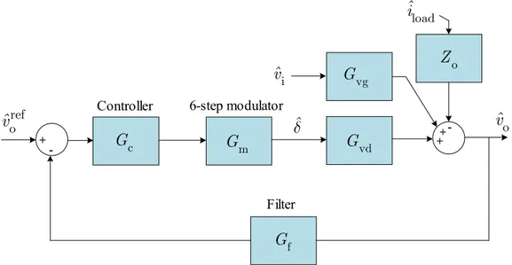
Small-signal frequency-domain modeling of converters is important in controller and filter designs, as well as stability and dynamic performance assessments [29]. Converter open-loop small-signal characteristics are generally defined by a set of standard transfer functions: the control-to-output transfer function Gvd, the input-to-output transfer function Gvg, the driving point ZD and null driving point ZN input impedances, and the output impedance Zo. For the stability analysis of
multiple converters interacting with other network components, it is also required to determine the closed loop small-signal characteristics of the converter such as the loop gain T and the closed-loop input and output impedances [30].
As for traditional ac-grids, the integration of power electronics in dc-grids also requires time-domain system-level studies such as general transient behavior, voltage regulation performance with load variations, transient stability, and short-circuit [28], [31]–[33]. Since the behavior of a converter depends on both its topology and its controller, closed-loop modeling of converters is necessary for system-level studies [34].
Each converter topology has its own particularities which must be considered in the modeling process. As it will be emphasized in this thesis, the application of well-known modeling strategies to the 3p-DAB converter is not trivial due to its dc-ac-dc structure, the different possible three-phase transformer connections and the higher number of switches compared to other IBDC topologies. As it will also be shown in this thesis, there is currently a lack of accurate small-signal models for stability analysis of the 3p-DAB in the literature. It is also the case for efficient and accurate large-signal models of the 3p-DAB for system-level studies in electromagnetic transient type (EMT-type) programs.
Furthermore, there is also limited literature on degraded-mode operation of the 3p-DAB converter. Recently, its has been identified in [35] that the 3p-DAB converter can be operated in a frozen leg degraded-mode. However, the analytical characterization of the converter behavior under all voltage and loading conditions is not trivial. Accurate characterization of the converter behavior in degraded-mode is an important topic for the development of reliable and resilient dc-grids [36], [37].
1.2 The three-phase dual active bridge (3p-DAB)
1.2.1 Control of the 3p-DAB
The basic three-phase dual active bridge (3p-DAB) topology is shown in Figure 1.3. The transformer voltage ratio M is used to match the nominal voltage levels between the two grids. Due to its three-phase structure, the 3p-DAB also allows using different winding connections (Y, Y-∆, and ∆-∆). It is, however, demonstrated in [24] that the Y-∆ transformer offers better performance in terms of stress on switches, transformer utilization, and filter capacitor requirements. The Y-∆ version (Figure 1.4 a)) has therefore been selected for investigation in this thesis.
Voltage control is performed by controlling the duty cycle of the primary and secondary bridges, and/or the phase-shift between the two bridges [38], [39]. Single-phase-shift (SPS) control has been the first proposed control method for the DAB converter. However, with SPS, both the 1p-DAB and the 3p-DAB have a limited ZVS soft-switching range under wide voltage and loading conditions [40]. For the 1p-DAB, extended-phase-shift (EPS) [41], dual-phase-shift (DPS) [42], and triple-phase-shift (TPS) [43] control strategies have been introduced to decrease the current stress, and improve the converter efficiency by extending its ZVS range. Due to the coupling between the three phases of the 3p-DAB, it has been shown that some TPS modulation methods [38] cannot be used without operating the 3p-DAB as a 1p-DAB converter. Even if it addresses the problem of poor partial load efficiency by extending the ZVS range, for the 3p-DAB, these strategies almost nullify the 3p-DAB advantages regarding the reduction of the output filter size [17]. The generic TPS modulation method of [43] has been used in [44] for the Y-Y 3p-DAB converter. While the results show a better efficiency at light load, it does not reduce the RMS current in the transformer as well as the maximum total losses at high load. It is not widely adopted in the literature and SPS still remains the most commonly used control method for the 3p-DAB. The Y-∆ 3p-DAB converter under study in this thesis is therefore operated using SPS control with a fixed switching frequency s 2 fs and a 180º (or 6-step) modulation method as shown in Figure 1.4 b) and c). The phase-shift between the gating signals applied to the two bridges is the variable used to regulate the voltage of either one of the two ports. For example, in forward operation ( 0 /2 ), the active power is transferred from the input bridge to the output bridge
such that vo is regulated to reach its reference value Voref . Reverse operation consists in reversing the sign of and regulating vi to reach a reference value Viref.
N A B C a b c : 1 M : 1 m ab v AN v A i B i C i ba i cb i ac i a i b i c i B
L
C L A L (a) (c) (b)Figure 1.4 : Control of the Y-∆ 3p-DAB converter under investigation
1.2.2 Variants of the 3p-DAB topology
Different topologies of the 3p-DAB are also being proposed with different objectives. In [45], a six-leg inverter is used on the low-voltage side with the main objective of increasing the converter current capability while preserving standard modulation techniques and DAB advantages. The six-leg structure results in three decoupled voltages applied on the low-voltage side of the three-phase transformer. AN v ab v S1 S1 1 0 1 0 6 2 ' 1
s
' 1s
V -+ 6-step modulator s 2 fs o v R i V c G f G ref o V m GMoreover, a 3p-DAB featuring a Y-∆ transformer and a current-tripler unit on the low-voltage side is proposed in [46] for increasing the converter conversion ratio while limiting the required transformer winding-ratio which has the negative effect of increasing the transformer leakage inductance and parasitic capacitance. The main drawback with the current-tripler version is that it does not offer ZVS on the low-voltage side. In [47] a current-fed topology is developed for achieving high efficiency over wide input voltage and loading ranges with a reduction in the circulation of reactive current in the Y-Y transformer.
The triple active bridge (TAB) topology using Y-YY and Y-Y∆ transformer configurations is also analyzed and the Y-Y∆ configuration is selected because it shows a better transformer utilization at high-power load [48], [49]. The TAB can be used to control the power flow between three different dc voltage sources, or to reduce the current through the output bridge switches by connecting the two output bridges in parallel.
1.3 Contributions
The main contributions of this thesis are summarized here. Each contribution is presented along with a literature review to clearly position this thesis with respect to previous work.
Contribution #1: Hybrid average modeling of three-phase dual active bridge converters for stability analysis [50]
The most popular technique to derive the analytical small-signal model of dc-dc converters is the state-space averaging (SSA) method [33], [51]. It is based on three main assumptions: 1) the switching ripple is small, 2) the ac variations are small, and 3) the modulation frequency m is much smaller than the switching frequency s [30]. It leads to a dc-averaged model of the converter. Due to the high-frequency ac-link in DAB converters, SSA has limitations in deriving an accurate small-signal model for DAB converters [52], [53]. SSA has been first applied to approximate the control-to-output Gvd, and the input-to-output Gvg transfer functions of the
3p-DAB in [54]. While it can be easily extended to the derivation of the output impedance Zo, there is currently no resource in the literature to evaluate the driving point input impedance ZD and the null
driving point input impedance ZN for 3p-DAB converters with SSA. These two transfer functions are necessary for the application of Middlebrook’s extra element theorem (EET) [55] which is broadly used by power electronic designers to analyze dc-dc converters in the presence of an additional input filter.
To overcome the limitations of the SSA method for DAB converters, generalized state-space averaging (GSSA) models [56] have been developed in [53], [57] and [58]. These models are not extended to the derivation of ZD and ZN. The derivation of ZN is particularly challenging for DAB
converters modeled with GSSA. The methodology presented in [52] is the first attempt to derive both ZD and ZN for 1p-DAB converters modeled with GSSA. The methodology requires determining the closed-loop input impedance Zinc with a dummy controller Gc before extracting
ZN by analytically removing the controller from the set of equations. The application of this methodology to 3p-DAB converters modeled with GSSA is neither shown nor trivial.
This thesis first contributes to the identification of the limitations of SSA in the modeling of 3p-DAB converters especially for the determination of ZD and ZN. While it will be shown that GSSA can be used to evaluate ZD, a new hybrid SSA and GSSA multi-input multi-output (MIMO) model,
which combines SSA and GSSA, is proposed to evaluate ZN. The proposed modeling approach is validated with time-domain simulations in Electromagnetic Transient Program (EMTP) [59]. Through the application of Middlebrook’s EET for additional input filter [55], it is demonstrated that the proposed approach can effectively reduce the number of time-domain simulation runs as well as the number of experimental tests required to predict degradation of dynamic performance and instability conditions. The use of Middlebrook’s theorem [55] not only guarantees stability, but also ensures that the introduction of an input filter does not substantially alter the converter transfer functions Gvd, Gvg, and Zo [60]. SSA, GSSA, and hybrid methodologies are also
thoroughly compared to provide a comprehensive review of their advantages, limitations, and overall performance.
Contribution #2: Large-signal modeling of three-phase dual active bridge converters for electromagnetic transient analysis in dc-grids [61]
As previously mentioned, large-signal modeling of the 3p-DAB converter is not trivial because of its dc-ac-dc structure, the various three-phase transformer connections and the higher number of switches compared to other IBDC topologies. The methodology presented in [62] is the first attempt to reduce the computation time for system-level studies with 3p-DAB converters in EMT-type programs. A discretized switching-function (SWF) model [63] in the αβ frame is implemented. It reduces the number of electrical nodes while preserving the switching-effect. However, it still requires time-steps in the range of 1/1000th of the switching period to maintain
numerical stability. The reduction in the computation time compared to the ideal-model approach is not shown and the reduction in the number of electrical nodes cannot be used alone as an indicator for the reduction in computation time.
The ideal-model approach is well known for the analysis of 3p-DAB converters and other topologies because its implementation using ideal switches is straightforward in circuit simulation tools. The ideal-model approach is a recognized reference for the validation of other models [28]. However, because the circuit topology is time-variant, the computation time is generally high for system-level studies. The SWF approach [63] has been proposed as an alternative methodology to ideal-model in which the converter circuit is replaced by controlled voltage and current sources. Since the circuit topology is now time-invariant, the SWF method reduces the computation
time[32]. However, because it keeps the switching-effect, small time-steps are still required. Averaged models [51], [56] are well known for neglecting the switching-effect and allowing the use of larger time-steps which significantly reduce the computation time.
In this thesis, a generalized averaging model (GAM) for time-domain simulation of 3p-DAB converters is developed, implemented and compared with the ideal, SWF [63] and SSA [51] methods in EMTP. In Figure 1.5, the simulation approaches investigated in this thesis are marked with a star (*). The ideal-model is used as a reference. Detailed-mode simulation in which detailed semiconductor models are used is not considered because such level of sophistication is generally not necessary for system-level studies.
This thesis contributes to provide a solution to the challenges in implementing a computational efficient and accurate model that enables time-domain system-level simulation of dc-grids with 3p-DAB converters. The reduced complexity and computation time of the proposed GAM model allow the efficient validation of future system-level control schemes in dc-grids. By comparing the performance of the developed GAM model in terms of transient response, computation time and frequency response with alternative modeling techniques, it also provides a complete comprehensive understanding of the advantages and limitations of the GAM approach applied to the 3p-DAB. A large-scale test system is also implemented to validate the performance of the GAM model for fault current and transient recovery voltage analysis in a practical size system.
Averaged-Model Detailed-Mode Behavior-Mode Ideal-Model Switching-Function*
Decreasing Level of Complexity Simulation of the 3p-DAB converter State-Space Averaging* Generalized-Averaging* (Ref.) (SWF) (GAM) (SSA)
Contribution #3: Open-phase fault-tolerant operation of the three-phase dual active bridge converter [paper conditionally accepted with major mandatory changes in IEEE Transactions
on Power Electronics]
In ac-grids, ac transformers are well known for their high reliability even in the presence of temporary or permanent overload conditions [64]. In dc-grids, the overall grid reliability can be significantly affected by the reliability of individual power electronic converters. The reliability of power electronic systems is in fact negatively affected by the higher number of components, including more vulnerable parts such as semiconductors and electrolytic capacitors. Failure of one of the components or subsystems generally lead to shutdown of the whole converter unit because most converters are not built with redundancy [37], [65].
Other than thermal management [66], oversizing of components, redundancy of converters, and fault-tolerant (FT) methods are recognized methodologies to improve the reliability of converters. Among these approaches, oversizing of components is the most used in the industry. However, while oversizing components such as filter capacitors is generally not a problem other than a probable reduction in the power density, oversizing semiconductors can negatively affect the efficiency and increase the overall cost of the converter. Besides, while it may reduce the occurrence of failures, it does not mean that the converter can resume operation upon fault detection. Instead of oversizing components, the traditional redundancy approach consists in adding extra parallel converters or modules, and/or adding redundant cells inside the converter structure for rapid reconfiguration of the faulty converter section. The redundancy approach is an expensive solution. FT operation is recognized to be more cost-effective than the redundancy approach [36]. FT operation means that a fault in a component or subsystem does not cause the overall system to malfunction [67]. In other words, degraded operation under post-fault conditions implies that the converter can continue operating with reduced performance metrics [37].
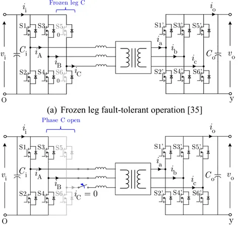
Because of its higher number of switches, it would be fair to argue that the reliability of the 3p-DAB converter is reduced when compared to other IBDC topologies, including the 1p-3p-DAB. However, it has been shown that the 3p-DAB converter can be operated in a frozen leg degraded-mode, i.e. with the two transistors of the same phase being deliberately opened by their gate driver internal protections, leaving their free-wheeling diodes self-commutated (Figure 1.6 a)) [35]. Because the free-wheeling diodes are left self-commutated, the analytical characterization of the
converter behavior in this degraded-mode is not trivial and leads to multiple cases to analyze which are functions of the converter voltage and loading conditions. The frozen leg operation of the 3p-DAB also leads to increased transformer current as well as a reduced power transfer capability for light and heavier load conditions. These loading conditions are characterized in [35] but are not generalized to all voltage and loading conditions. Moreover, due to the complexity in deriving an analytical model, the impacts on the ZVS capabilities, controller sizing, dynamic response, and stability are not validated.
In response to this challenge, the research contributions of this thesis are as follows. First, it is proposed to open the faulty-phase side such as it eliminates the interaction of the faulty-leg free-wheeling diodes (Figure 1.6 a)). As a result, it is possible to characterize the steady-state and transient operations of the 3p-DAB with one phase open for all voltage and loading conditions. It allows evaluating the major impacts of open-phase fault-tolerant operation as well as presenting key design considerations for a successful open-phase FT operation. Furthermore, the results also revealed that open-phase operation can provide increased power transfer capability and reduced circulating current as compared to frozen leg proposed in [35].
(a) Frozen leg fault-tolerant operation [35]
(b) Proposed open-phase fault-tolerant operation
Figure 1.6 : Comparison of the fault-tolerant modes of the 3p-DAB
i v Ci i i A i B i C i a i b i c i Co o i o v S1 S2 S3 S4 S5 S6 S1 S2 S3 S4 S5 S6 0 0 Frozen leg C O y i v Ci i i A i B i C 0 i a i b i c i Co o i o v S1 S2 S3 S4 S5 S6 S1 S2 S3 S4 S5 S6 Phase C open y O
1.4 Methodology and limits
1.4.1 Methodology
The design and integration process of power electronic converters such as the 3p-DAB requires investigations with different abstraction levels [68]. The main objective of this thesis is to develop and validate accurate models for integration analyses of 3p-DAB converters in dc-grids. A hierarchical modeling, simulation, testing and analysis methodology is used. Time-domain simulation in EMTP and experimental results on a small-scale closed-loop EPC2022 gallium nitride (GaN)-based Y-∆ 3p-DAB converter are also provided. Four (4) different converter design parameter sets are used in this thesis. This is explained by the evolution of the project over time and the necessity to address comments in the publication process prior to the writing of this thesis. Their main parameters are summarized in Appendix A and additional details on the design and fabrication of the small-scale prototype are provided in Appendix B.
The methodology is summarized as follows:
1. Steady-state analysis: A generalized phasor-domain method based on the first harmonic approximation (FHA) method [12] combined with Mordey’s V-curve theory for synchronous machines [69] is first proposed for gaining understanding and physical insight. Then, the piecewise-linear modeling (PLM) approach [12], [24] is used for the determination of the parameters of the converter models, and for designing the small-scale prototype. PLM is also used for evaluating the converter operating point, the power transfer relationships, the ZVS boundaries, and for the sizing of the output capacitor. PLM is a necessary step for the development and implementation of small- and large-signal models. 2. Small-signal frequency-domain analysis: State-space averaging (SSA) and generalized
state-space averaging (GSSA) small-signal models are derived for the calculation of all the open-loop transfer functions of the Y-∆ 3p-DAB converter (Gvd, Gvg, ZD, ZN, and Zo).
Both models are then compared and validated with time-domain simulations in EMTP. While GSSA is used to evaluate ZD, a hybrid SSA and GSSA input multi-output (MIMO) model is proposed to evaluate ZN. The developed models are used for the
design of the closed-loop controller, and for dynamic performance and stability assessments using MATLAB/Simulink.
3. Large-signal time-domain modeling and simulation: A generalized averaging model (GAM)of the Y-Δ 3p-DAB converter is developed, implemented and compared in closed-loop with the ideal, switching-function (SWF) and SSA methods applied to the 3p-DAB in EMTP. The performance of the GAM model is analyzed in terms of transient response, computation time and frequency response. A large-scale test system is also implemented to validate the performance of the GAM model for system-level transient fault current and transient recovery voltage analyses.
4. Open-phase fault-tolerant analysis:Steady-state analysis based on the PLM approach is performed to characterize the converter in open-phase operation and evaluate the impacts on the converter steady-state characteristics. Open-phase operation is also compared with frozen leg [35] and normal operations. Moreover, small-signal frequency-domain analysis using SSA and GSSA methodologies is performed to design a suitable closed-loop controller for both normal and open-phase operations as well as to assess the impacts on the converter stability and dynamic performance.
1.4.2 Limits
In this thesis, the converter under study is the Y-∆ 3p-DAB operated using single-phase-shift (SPS) control with a fixed switching frequency s and a 180º (or 6-step) modulation scheme. The results are not extended to other emerging modulation methods. The converter is assumed lossless for steady-state, small-signal and large-signal analyses. Information on loss analysis for the 3p-DAB converter can be found in [68], [70]–[72]. The transformer magnetizing inductance and the presence of snubber capacitances are neglected. The switches are assumed ideal. The dead-time between the upper and lower switches is also neglected because it increases drastically the complexity in modeling the 3p-DAB converter [73]. The result is the assumption of an ideal transition of the current from the free-wheeling diodes to the transistors during the ZVS turn-on events. Furthermore, only forward operation and the Y-∆ transformer are considered but the generalization to other transformer connections is discussed. The load is assumed to be purely resistive.
1.5 Thesis outlines
The structure of this thesis is mainly oriented to follow the methodology and to expose the development specific to each of the contributions defined in section 1.3.
In Chapter 2 – Steady-State Analysis, steady-state modeling of the 3p-DAB converter is used for sizing and for providing a general understanding of the converter operating principles. It is a necessary step to small-signal (Chapter 3) and large-signal (Chapter 4) analyses.
In Chapter 3 – Small-Signal Frequency-Domain Analysis, small-signal models of the 3p-DAB are developed, validated and implemented. They are used for closed-loop controller design, as well as small-signal stability assessment and dynamic performance analysis in MATLAB/Simulink. In Chapter 4 – Large-Signal Time-Domain Simulation, a generalized average model (GAM) is developed, validated and implemented. It enables closed-loop system-level simulation of dc-grids with 3p-DAB converters in EMTP.
In Chapter 5 – Open-Phase Fault-Tolerant Operation, steady-state, small-signal and transient analyses are performed to enable the successful operation of 3p-DAB converters in open-phase fault-tolerant condition.
In Chapter 6 – Conclusions and Recommendations, the main conclusions of this thesis are presented along with recommendations for future area of research in modeling, simulation, and analysis of the 3p-DAB converter in both normal and fault-tolerant operations.
CHAPTER 2
STEADY-STATE ANALYSIS
In this chapter, steady-state modeling of the 3p-DAB converter is performed for supporting the selection of the parameters of the converter models as well as for assisting the selection of the components for the small-scale prototype. It also presents the main steps for the calculation of the converter operating point, the power transfer relationships, and the zero-voltage switching (ZVS) regions. This step is necessary for the development of small- and large-signal models as well as for the analysis of the converter in degraded-mode.
2.1
First harmonic approximation (FHA) in phasor-domain
2.1.1 Motivation
The steady-state analysis of the DAB is generally performed using the piecewise-linear modeling (PLM) approach. As it will be seen in section 2.2, this approach is a demanding task for 3p-DAB converters. To simplify the analysis, the 3p-DAB can also be analyzed using the first harmonic approximation (FHA) in the phasor-domain [12], [74]. It consists in replacing the input and output bridges by voltage sources at the switching frequency s and the transformer by its equivalent leakage reactance Xs. Using this model, the power transfer relationship of the 3p-DAB is similar to the power-angle relationship of synchronous machines. This method can also be used to approximate the input and output bridge ZVS ranges.
In this thesis, a generalized FHA phasor-domain modeling method for steady-state analysis of 3p-DAB with single-phase-shift (SPS) control has been developed. A set of general and simplified equations has been developed and a useful diagram for first converter design has been developed in physical and per-unit quantities. The FHA method has been generalized for different transformer connections and validated using time-domain simulations.
The FHA method combined with the use of the developed diagram allows approximating the RMS and peak currents as well as the ZVS regions for given converter specifications. It also provides a means to understand the general operating principles of the 3p-DAB converter. Unlike PLM, the FHA method results in a single set of equations which does not depend on the transformer connection and the control phase-shift operating range.
2.1.2 Model development
The transformer is first replaced by its equivalent primary-referred leakage reactance Xs s sL . As seen in Figure 2.1, the voltages applied by the input and output bridges, vAN and van'
respectively, are modeled by equivalent phasor-domain voltage sources VAN and Van' at the switching frequency s. The equivalent transformer current IAobtained from the phasor-domain analysis is close to the time-domain current iA which is almost sinusoidal owing to the three-phase structure. The resulting FHA phasor-domain circuit and phasor diagram are given in Figure 2.2.
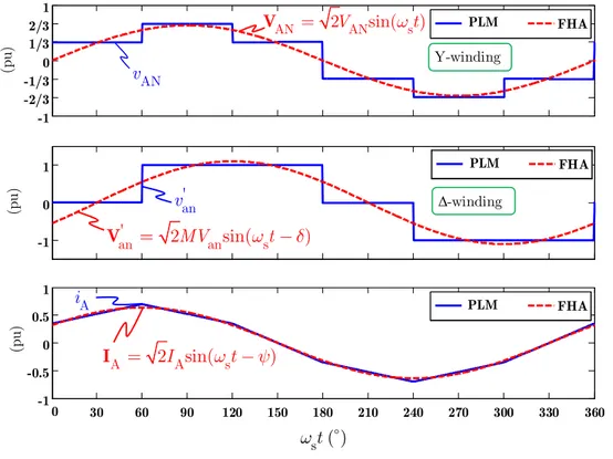
Figure 2.1 : Comparison of PLM and FHA waveforms for the Y-Δ transformer
AN VAN 0 V P > 0 Q > 0 ' ' an Van V A IA I s jX AN V A I jX Is A ' an V
(a) Equivalent single-phase circuit (b) Equivalent phasor diagram Figure 2.2 : FHA model in physical quantities
30 60 90 120 150 180 210 240 270 300 330 360 -1 -2/3 -1/3 0 1/3 2/3 1 Piecewise FHA 30 60 90 120 150 180 210 240 270 300 330 360 -1 0 1 v' ab 30 60 90 120 150 180 210 240 270 300 330 360 -1 -0.5 0 0.5 1 t ( ) Piecewise FHA Piecewise FHA 0 0 0 AN v AN 2VANsin( st) V ' an v ' an 2MVansin( st ) V A i A 2 sin(IA st ) I (p u) (p u) (p u) st( ) PLM PLM PLM Y-winding Δ-winding
The phasor-diagram is defined in generating convention such that active and reactive powers are positive when flowing from VAN to Van' . The input voltage phasor VAN is taken as the reference, which implies that the modulator is synchronizing the output bridge with respect to the input bridge.
AN
V is comparable to the synchronous generator internal field excitation in the equivalent machine model. The output bridge voltage Van' is equivalent to the network voltage. The phase-shift is equivalent to the power angle of the synchronous machine such that, a positive value of means that the active power is transferred from VAN to Van' (forward operation). Conversely, a negative value of means that the active power is transferred from Van' to VAN(reverse operation). The angle is the angle between the transformer line current IA and the output bridge voltage Van' such that the value of cos( ) is similar to the power factor of the synchronous machine with respect to the network. The angle is the angle between the transformer line current IA and the input bridge voltage VAN. Based on these definitions, the active and reactive power equations for the input and output bridges are written as,
i 3 AN Acos( ) i 3 AN Asin( )
P V I , Q V I (2.1)
' '
o 3 an Acos( ) o 3 an Asin( )
P V I , Q V I (2.2)
For the equivalent single-phase circuit of Figure 2.2 a), it is also well known that the power transfer equation (or power-angle equation) is given by,
' AN an i o s 3 sin( ) V V P P P X (2.3)
Because both the voltage and the current are non-sinusoidal, it is expected that both the fundamental and harmonic components contribute to the active power flow. However, as the harmonic order increases, the equivalent reactance of the transformer also increases, which reduces the power transfer capability of the transformer at higher harmonics. This mainly explains why FHA can be used to evaluate the power transfer relationship of 3p-DAB converters in a similar way to the power-angle relationship of synchronous machines connected to an equivalent network at the fundamental frequency s.
In the 3p-DAB, reactive current needs to circulate through the transistors free-wheeling diodes to provide ZVS at turn-on of the transistors. On the phasor diagram of Figure 2.2 b), it means that IA
must lie between the input voltage VAN and the output voltage Van' [12]. In other words, IA must lag VAN for ZVS at the input bridge (see example in Figure 2.3), and similarly, IAmust lead Van' for ZVS at the output bridge. Physically, it means that both bridges are providing reactive power to the transformer leakage reactance Xs. The equivalent phasor diagrams at the ZVS boundaries for the input and output bridges are given in Figure 2.4 a) and b) respectively. Mathematically, it means that 0 (i.e. cos( ) = 1) at the ZVS boundary of the input bridge and 0 (i.e.
cos( ) = 1) at the ZVS boundary of the output bridge. Using the phasor diagrams of Figure 2.4 a) and b),the ZVS boundaries for both bridges are evaluated. For the input bridge it yields to,
' 2 2 an AN A s (V ) (V ) I X (2.4)
and for the output bridge it leads to,
2 ' 2 AN an A s (V ) (V ) I X (2.5)
As for the synchronous machine, the maximum power transfer in (2.3) occurs when 90 . In this condition, the equivalent phasor diagram is shown in Figure 2.4 c), and the current IA at the maximum power transfer boundary is evaluated as,
2 ' 2 AN an A s (V ) (V ) I X (2.6)
Another useful relationship is the equation which relates the transformer current IAto the input AN
V and output Van' voltages for different phase-shift angles . It is given by,
' 2 2 AN an AN A s (V cos( ) V ) (V sin( )) I X (2.7)
Finally, the equation which relates the transformer current IAto the input VAN and output Van'
voltages for different output power set-points Po is established. This relationship is equivalent to Mordey’s V-Curve for synchronous machines [69] which is widely used for design and testing of synchronous machines. It can be demonstrated that the resulting relationship for the 3p-DAB is given by,
2 2 ' 2 ' 2 an o s A ' AN ' an o s an an 3 1 ( ) ( ) 3 3 V P X I V V P X V V (2.8)
Figure 2.3 : Typical waveforms with ZVS in the input bridge (Y-Δ transformer)
Equations (2.4)–(2.8) need to be written in terms of the dc input and output voltages (Vi and Vo) to be useful for the analysis of 3p-DAB converters. Fourier decomposition of the waveforms for Y- and ∆-windings is used to obtain the amplitude of the phasors VAN and Van' in terms of Vi and
o V respectively, AN i 2 2 V V (2.9) ' an an o 2 2 V MV M V (2.10)
The peak current can be approximated by, pk
A 2 A
I I (2.11)
From the input bridge current, the output bridge current can also be obtained with,
a A
Moreover, the per-unit model is a generalization of the physical quantities model which allows more flexibility in the analysis of the 3p-DAB converter. The per-unit model is obtained from the physical quantities model by using the following base,
' ' 2 ' an an b an b b b b b s s s ( ) , V , V , V V I S V I Z X X X (2.13)
For convenience, the ratio between the input and output voltages is also expressed as,
AN i ' o an V V D MV V (2.14) AN V A I s A jX I ' an V AN V A I s A jX I ' an V AN V A I s A jX I ' an V
(a) At ZVS boundary input bridge
(b) At ZVS boundary output bridge (c) At maximum power transfer
Figure 2.4 : Equivalent phasor diagrams
2.1.3 Model validation and analysis of the results
The equations of the generalized FHA model are validated for three different transformer connections (Y-Y, ∆-∆, and Y-∆) using time-domain simulations in EMTP. The results are shown in Figure 2.5 for the Y-Y and ∆-∆ transformers and Figure 2.6 for the Y-∆ transformer.
From the results obtained in Figure 2.5 and Figure 2.6, it is concluded that the FHA modeling method is accurate to evaluate the constant output power Po equation given in (2.8). It is also precise to determine the constant phase-shift equation given in (2.7) which also includes the maximum power transfer equation at 90 given in (2.6). The maximum error between the FHA model and time-domain simulations for the calculation of the RMS current is lower than 1%. For
the calculation of the peak current, the maximum error is 10%. This is explained by the fact that the current is not perfectly sinusoidal in the transformer.
Figure 2.5 : Validation of the FHA design diagram for the Y-Y and ∆-∆ transformers
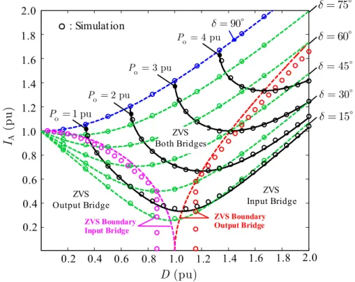
Figure 2.6 : Validation of the FHA design diagram for the Y-∆ transformer 0.2 0.4 0.6 0.8 1 1.2 1.4 1.6 1.8 2 0.2 0.4 0.6 0.8 1 1.2 1.4 1.6 1.8 IA ( p u ) d (pu) P1 = 1 pu P 2 = 2 pu P3 = 3 pu = 90° = 60° = 45° = 30° = 15° = 75° P4 = 4 pu : FHA Model : Piecewise-linear (Simulation) ZVS Boundary
Input Bridge ZVS Boundary Output Bridge
IA (p u ) 0.2 0.4 0.6 0.8 1.0 1.2 1.4 1.6 1.8 2.0 D (pu) 0.2 0.4 0.6 0.8 1.0 1.2 1.4 1.6 1.8 2.0 : Simulation 75 60 45 30 15 o 1 pu P o 2 pu P o 3 pu P o 4 pu P 90 ZVS Both Bridges ZVS Input Bridge ZVS Output Bridge 0.2 0.4 0.6 0.8 1 1.2 1.4 1.6 1.8 2 0.2 0.4 0.6 0.8 1 1.2 1.4 1.6 1.8 IA ( p u ) d (pu) = 75° = 15° = 30° = 45° = 60° = 90° P3 = 3 pu P 2 = 2 pu P 1 = 1 pu : FHA Model : Piecewise-linear (Simulation) P4 = 4 pu ZVS Boundary Input Bridge ZVS Boundary Output Bridge D (pu) o 1 pu P o 2 pu P o 3 pu P 90 75 IA (p u ) 0.2 0.4 0.6 0.8 1.0 1.2 1.4 1.6 1.8 2.0 0.2 0.4 0.6 0.8 1.0 1.2 1.4 1.6 1.8 2.0 o 4 pu P : Simulation 60 45 30 15 ZVS Both Bridges ZVS Input Bridge ZVS Output Bridge
It is also observed in Figure 2.5 and Figure 2.6 that the FHA modeling approach is less accurate to evaluate the input and output bridges ZVS boundaries at low output power. The maximum error between FHA and time-domain simulations is 15 % for the Y-∆ transformer, and 8 % for the Y-Y and ∆-∆ transformers. However, two important observations must be made. First, FHA leads to a conservative evaluation of the ZVS regions. This means that the ZVS regions evaluated using FHA are smaller than expected with time-domain simulations. Second, FHA gives a good estimation at high output power. The identification of the ZVS regions is generally more critical at high output power. The error between FHA and time-domain simulations is explained by the fact that harmonic distortion in the transformer current leads to errors in the evaluation of the current zero-crossing; ZVS occurs in the input bridge if iA 0 at turn-on of S1 as shown in Figure 2.3, and ZVS occurs in the output bridge if ia 0 at turn-on of S1.
2.1.4 Application to the experimental prototype (model 4)
The FHA method combined with the use of the developed diagram allows approximating the RMS and peak currents as well as the ZVS regions for given converter specifications. It is an important step for the development of a hardware prototype and, to a lesser extent, to the implementation of simulation models. For this reason, the Y-Δ 3p-DAB prototype (model 4) is used in this section as a design example. For a constant output voltage Vo 24 V,the design diagrams for two different switching frequencies fs 50 kHz and fs 100 kHz are given in Figure 2.7. The testing zone represents the operating zone for which simulations and experiments have been conducted.
Important conclusions regarding the 3p-DAB operating principles can also be drawn from the results in Figure 2.7. First, it is possible to see that, for the same amount of active power transferred, minimum RMS current operation occurs at the output bridge ZVS boundary. High reactive circulating current increases the transformer losses and decreases the transformer utilization, such that, for the same output power, it is desirable to reduce the amount of reactive current while keeping ZVS at both bridges. Furthermore, from a design standpoint, the leakage inductance Ls
should be selected such that maximum power transfer is possible for the entire voltage operating ranges. For instance, in Figure 2.7 a), for Vo 24 Vand fs 50 kHz, it is concluded that the converter can be operated at Po 250 W for the entire range of input voltage Vi (18 V to 30 V)
without reaching the maximum power transfer limit 90 . It is not the case if fs 100 kHz as seen in Figure 2.7 b). This is because the power transfer capability of the 3p-DAB decreases as the switching frequency fs increases and as the input voltage Vi decreases. This can be seen by rewriting (2.3) using (2.9) and (2.10),
i o o 2 s s 6 3 sin( ) mVV P L (2.15)
In Figure 2.7, it is also possible to perform a preliminary assessment of the ZVS boundaries for both bridges. First, it can be observed that, under low load conditions, ZVS is not guaranteed at the input bridge for low input voltage Vi, and at the output bridge for high input voltage Vi. At higher power set-points Po, the ZVS range increases up to a point where the main limitation on the converter design becomes the maximum phase-shift angle 90 . Also note that, for the same output power Po, the region where both bridges are ZVS tends to increase at low power as the switching frequency fs is increased.
The maximum RMS current expected for the hardware prototype is IA 12 5 A (. IApk 17 7 A).