HAL Id: tel-02138109
https://tel.archives-ouvertes.fr/tel-02138109
Submitted on 23 May 2019HAL is a multi-disciplinary open access archive for the deposit and dissemination of sci-entific research documents, whether they are pub-lished or not. The documents may come from teaching and research institutions in France or abroad, or from public or private research centers.
L’archive ouverte pluridisciplinaire HAL, est destinée au dépôt et à la diffusion de documents scientifiques de niveau recherche, publiés ou non, émanant des établissements d’enseignement et de recherche français ou étrangers, des laboratoires publics ou privés.
distribution network for adiabatic logic
Nicolas Jeanniot
To cite this version:
Nicolas Jeanniot. Design and optimization of power-clock generator and distribution network for adiabatic logic. Optics / Photonic. Université Montpellier, 2018. English. �NNT : 2018MONTS068�. �tel-02138109�
1
THÈSE POUR OBTENIR LE GRADE DE DOCTEUR
DE L’UNIVERSITÉ DE MONTPELLIER
En Systèmes Automatiques et Micro-Électroniques École doctorale : Information, Structures, Systèmes
Unité de recherche LIRMM
Conception et optimisation d’une alimentation-horloge et
d’un réseau de distribution pour la logique adiabatique.
Présentée par Nicolas J
EANNIOTle 28 Novembre 2018
Sous la direction de Aida TODRI-SANIALet Gaël PILLONNET
Devant le jury composé de
Bruno ALL ARD Professeur des universités Ampère-INSA de Lyon Rapporteur
Marie-Minerve LOUËRAT Chargée de recherche LIP6-Université Pierre et Marie Curie Rapportrice
Guy CATHEBRAS Professeur des universités LIRMM-Université de Montpellier Président du jury
Catherine BRU-CHEVALLIER Directrice de recherche INL-INSA de Lyon Examinatrice
Aida TODRI-SANIAL Chargée de recherche LIRMM-Université de Montpellier Directrice de thèse
Gaël PILLONNET Chercheur CEA-LETI-Université Grenoble-Alpes Co-directeur de thèse
Hervé FANET Chercheur CEA-LETI-Université Grenoble-Alpes Invité
i
A ma famille et mes amis, Qui m’ont soutenu tout au long de ce voyage,
“Ce n’est pas assez d’avoir l’esprit bon, mais le principal est de l’appliquer bien.” René Descartes
Remerciements
Cette thèse est l’accomplissement de trois ans de réflexion, de recherche mais surtout de relations humaines. Ce projet m’aura fait grandir tant scientifiquement qu’humainement et c’est pour cela que je souhaiterais remercier les personnes qui m’ont donné du temps et nourri ma réflexion.
Mes tous premiers remerciements vont à mes principaux guides durant ces 3 ans : Aida Todri-Sanial, directrice de cette thèse, pour m’avoir challengé, soutenu et avoir toujours cru en moi; ainsi que Gaël Pillonnet, co-directeur de thèse, pour son aide, nos discussions hebdomadaires et son indéfectible palais pour le mauvais Viognier.
Je souhaiterais remercier Marie-Minerve Louerat et Bruno Allard pour avoir accepté d’être les rapporteurs de cette thèse ainsi que Siegfried Karg et Hervé Fanet. Ce manuscrit a gagné en qualité grâce à leurs commentaires et leurs critiques constructives. Je remercie Cather-ine Bru-Chevallier et Guy Cathébras, qui aura été la première victime de mes réflexions sur la logique adiabatique, pour avoir accepté d’examiner cette thèse.
Cette thèse a été subventionnée par l’agence nationale pour la recherche. Je tiens à re-mercier tous les membres de notre groupe de projet ADIANEMS2 pour m’avoir inclus dans cette belle aventure qui m’aura permis de découvrir le fonctionnement et le procédé de fabrication des MEMS, les contraintes de la logique capacitive ou encore les avantages de l’électronique haute température. Merci à Philippe Basset, Nicolas Pavy et Hatem Samaali de l’ESIEE et Yann Perrin et Ayrat Gasisultanov du CEA.
Pendant 2 ans et demi, j’ai vécu à Montpellier et j’ai eu l’opportunité de travailler au LIRMM. Je me dois de remercier Caroline Lebrun et Nicolas Serrurier Gourves pour m’avoir accueilli, avoir facilité toutes mes démarches administratives et de manière générale, avoir toujours été là pour m’aider. Je remercie ensuite Jérémie Salles pour m’avoir aidé
à décrypter les diverses installations de Cadence, les règles obscures de DRC ou encore de m’avoir appris à casser des antennes. Merci aussi à mon groupe de travail pour nos discussions, nos cafés, nos réflexions, nos partages qui je l’espère nous aura tous permis d’avancer pour le mieux. Merci à Rongmei Chen, El Mehdi Kaoukab, Jie Liang, Reetu Raj Pandey et Liuyang Zhang. Merci aussi à tous les gens du couloir 2.1, pour leur bonne humeur, leur écoute et leur dynamisme en particulier Geneviève Carrière et Mylène Guey-dan. Merci aussi à ce groupe de microb qui m’a rendu la vie à Montpellier si facile, pour les repas, les soirées, les parties d’échec, les raclettes ... Merci à vous,entre autres, Guillaume Aiche, Maxence Blond, Quentin Boehler, David Cavard, Maxime Cosi, François Leborne, Alonso Sanchez, Joao Santos, Jun Sun et Julien Toulemont.
Je remercie aussi le laboratoire LGECA du CEA-LETI qui m’a accueilli pendant 6 mois pour me permettre de commencer mon layout après m’avoir permis de réaliser mon PFE dans leurs locaux.
Je tiens également à remercier 2 montpelliérains d’adoption qui m’ont supporté pendant ces 3 ans, Julien Fillon pour avoir été ma bouée de sauvetage en arrivant sur Montpellier et dont nos séances de sports plus ou moins hebdomadaires me manqueront ainsi que Jean-Luc Tessier qui a l’aide de plantes médicinales aura su soigner mon spleen grenoblois. En dernier lieu, je remercie ma famille qui m’a toujours soutenu dans mes décisions et m’a encouragé à tracer ma propre voie. Je me dois aussi de remercier ma compagne, Marlene Taheulle, pour m’avoir suivi jusqu’à Grenoble, puis laissé partir à Montpellier et surtout encouragé tout au long de ce parcours.
Résumé
La densité de puissance est devenue l’une des principales préoccupations lors de la con-ception d’un système numérique. Comme pour tous les systèmes embarqués, chaque nouvelle génération de système numérique a plus d’applications que la précédente et ex-ige en fin de compte une plus grande densité de puissance. C’est pourquoi de nombreux chercheurs et de concepteurs industriels se sont penchés sur de nouvelles méthodes de réduction de la consommation électrique des circuits numériques.
De plus, du point de vue de la consommation énergétique, avec l’augmentation du nom-bre d’objets connectés, de centres de données et de dispositifs de communication, ces ap-pareils électroniques pourront représenter jusqu’à 51% de la demande énergétique mondi-ale en 2030. Pour limiter l’augmentation de la consommation énergétique, il y a trois axes de recherches : développer de nouveaux composants, développer de nouvelles techniques de conception au niveau des portes, des circuits et des systèmes ainsi que développer de nouvelles architectures.
Cette thèse se concentre sur un style de conception de portes alternatif, la logique adia-batique. Cette logique peut réduire la consommation d’énergie dynamique [1]. La plupart de la consommation d’énergie dans les circuits numériques provient des dissipations dy-namiques, cette dissipation vient de la façon dont sont alimentées les portes numériques. L’énergie nécessaire pour charger les portes numériques conventionnelles sont dissipées deux fois, à la charge, la même quantité d’énergie stockée dans la capacité équivalente est dissipée dans la porte et ensuite à la décharge où l’énergie est dissipée à la masse. L’essence de la logique adiabatique est de charger la porte logique avec une rampe puis de la décharger vers l’alimentation. Pour économiser de l’énergie, la charge et la décharge doivent être effectuées à la fréquence la plus basse possible. Même si le principe adiaba-tique est connu depuis les années 70, le compromis entre la consommation énergéadiaba-tique
et la fréquence n’était pas particulièrement intéressant. Avec l’émergence de nouveaux transistors comme les transistors à effet de champ à base de nanotubes de carbone, CNT-FET, les interrupteurs nano-électro-mécaniques, NEMS, ou encore les transistors à effet de champ à fente verticale, VeSFET, les recherches sur la logique ont gagné un nouvel intérêt. L’une des particularités de la logique adiabatique est que l’alimentation sert également d’horloge et est appelée alimentation-horloge. Le premier objectif de cette thèse est d’étudier comment générer le signal d’alimentation-horloge, puis de proposer une topolo-gie d’alimentation-horloge afin de maximiser le rendement énergétique d’un circuit adia-batique.
En conception intégrée, un des problèmes concerne l’intégrité des signaux d’alimentation et d’horloge. Les problèmes potentiels d’intégrité proviennent des parasites du réseau de distribution d’énergie et celui de distribution d’horloge. Pour les circuits adiabatiques, le réseau de distribution d’énergie et celui de distribution d’horloge sont combinés dans un réseau de distribution d’alimentation-horloge. Le second objectif de cette thèse est d’étudier l’impact du réseau de distribution sur le rendement énergétique du circuit adia-batique puis de proposer une optimisation de ce même réseau de distribution.
Cette thèse a été financée par l’ANR, avec le projet ADIANEMS2 (numéro de subven-tion : ANR-15-CE24-0013). Ce projet est une collaborasubven-tion entre l’ESIEE, le CEA-LETI et le LIRMM. Les objectifs du projet sont d’évaluer les économies d’énergie potentielles d’un circuit adiabatique à l’aide de nanosystèmes électromécaniques, NEMS. L’objectif du LIRMM est de développer une alimentation-horloge et son réseau de distribution. La recherche de l’ESIEE se porte sur la conception de nouveaux NEMS pour leur utilisation dans la conception de portes logiques adiabatiques. Le rôle du CEA-LETI est de concevoir de nouvelles portes logique en utilisant ces NEMS.
Cette thèse est divisée en 7 chapitres. Elle comporte une introduction et une conclusion et 5 chapitres sur le travail de thèse. Nous allons résumer l’ensemble des contributions de cette thèse chapitre par chapitre.
Le chapitre 2 présente l’état de l’art de la logique adiabatique ainsi que les problèmes rencontrés par l’utilisation des portes logiques adiabatiques conçues avec des transistors CMOS. La dissipation d’énergie d’une porte logique adiabatique est la somme de trois dis-sipations : la dissipation adiabatique, la dissipation due aux fuites et celle due à la ten-sion de seuil. La dissipation adiabatique est proportionnelle à la fréquence, tandis que la dissipation due aux fuites est inversement proportionnelle à celle-ci. Il existe donc une fréquence optimale pour limiter ces deux dissipations. La dissipation due à la tension de seuil est une dissipation indépendante de la fréquence, qui provient de la décharge incom-plète des portes logiques dans l’alimentation-horloge.
Grâce à l’état de l’art, nous sélectionnons la logique adiabatique PFAL, pour réaliser notre étude sur l’alimentation-horloge et son réseau de distribution. Nous optimisons la
dissi-vii
pation d’énergie d’une porte logique PFAL avec les paramètres suivants : le nœud tech-nologique CMOS, la tension de seuil et la tension d’alimentation. Grace à cette optimisa-tion, nous sélectionnons des transistors CMOS Low-VTH45nm pour concevoir un tampon
PFAL, qui dissipe idéalement 13aJ par cycle à une fréquence optimale de 5MHz.
Le chapitre 3 présente le réseau de distribution d’alimentation-horloge, PCN, qui est si-multanément le réseau de distribution d’énergie et le réseau de distribution d’horloge. Un état de l’art sur ces réseaux pointe les problèmes qu’un PCN peut avoir : le retard du signal de l’horloge, la chute de tension IR et la sensibilité aux bruits du signal d’alimentation-horloge.
Nous avons divisé l’étude du PCN en deux étapes : nous étudions son impact sur une porte unique, puis sur de multiples portes.
Grâce à l’étude du PCN sur une seule porte, nous modélisons la dissipation d’énergie de la porte par rapport à sa propre résistance et capacité, à la résistance du PCN et à la fréquence de fonctionnement. Afin de montrer l’impact du PCN, nous introduisons trois contraintes sur la résistance du PCN : R5, R999et RCRIT. R5limite la dissipation d’énergie
supplémen-taire maximum due au PCN à 5% de la dissipation d’énergie d’une porte idéale. R999est la
valeur maximale de la résistance du PCN, où la porte logique est complètement chargée à la fin de la phase de maintien. Enfin, RCRITest la valeur maximale de la résistance du PCN,
où la porte adiabatique dissipe moins d’énergie qu’une porte classique idéale. Cette étude nous permet de nous assurer que la dissipation adiabatique peut être exprimée comme ci-après : EAL= 2RCT CVDD2 où la résistance est la somme des résistances de la porte et du
PCN.
L’étude de l’impact du PCN sur de multiples portes nous a permis d’établir des lignes direc-trices pour concevoir et dimensionner le PCN afin d’optimiser la dissipation énergétique. À partir de cette étude, nous obtenons la valeur maximale de la résistance et de la capac-ité du PCN en prenant en compte la fréquence de fonctionnement, le nombre de portes et à la dissipation d’énergie supplémentaire tolérable. Avec ce guide de conception, nous proposons de dimensionner le PCN afin d’avoir des valeurs de résistance et de capacité parasites inférieures aux valeurs maximales que nous avons obtenues.
Le chapitre 4 présente l’étude des alimentations-horloges. L’alimentation-horloge génère un signal à 4 phases. L’état de l’art sur ces alimentations nous indique qu’il y a deux familles d’alimentation-horloge : celles à base de capacités ou celles résonantes. Nous avons choisi d’étudier les alimentations résonantes.
Nous étudions des topologies pour l’alimentation-horloge dans deux cas différents. Dans le premier cas, l’alimentation-horloge doit alimenter un pipeline composé de tampons PFAL en CMOS 45nm, avec une tension d’alimentation de 0.5V et une fréquence de fonctionnement de 5MHz. Dans le second cas l’alimentation-horloge doit alimenter un
pipeline composé de tampons PFAL en CMOS 65nm, avec une tension d’alimentation de 1, 2V et une fréquence de fonctionnement de 2, 5MHz.
Nous proposons une nouvelle topologie d’alimentation-horloge à base d’inductance. La nouveauté réside dans la synchronisation de chaque alimentation-horloge. Nous opti-misons cette topologie afin de minimiser la dissipation d’énergie.
Dans le premier cas, le résultat est qu’un pipeline CMOS 45 nm composé d’un tampon PFAL dissipe 167aJ par cycle à 5MHz, soit 2, 9 fois moins qu’un pipeline composé d’un tampon conventionnel en CMOS 45 nm. Toutefois, à la fin de la phase d’évaluation, la charge directe de la porte est plus importante que prévu, ce qui nuit à le rendement én-ergétique.
Pour comprendre pourquoi la dissipation énergétique est plus importante que prévue, nous étudions les différences entre notre modèle et les simulations. Le résultat de cette étude est que la résistance de la porte ne peut pas être modélisée comme une résistance à valeur constante lorsque la tension d’alimentation n’est pas à sa valeur nominale.
C’est pourquoi nous étudions le second cas. Après optimisation, un pipeline composé d’un tampon PFAL en CMOS 65nm dissipe 433aJ par cycle à 2, 5MHz, soit 3, 23 fois moins que le pipeline composé d’un tampon conventionnel en CMOS 65 nm.
Le chapitre 5 présente la réalisation d’un circuit adiabatique, conçu en CMOS 65nm. Il est composé d’un pipeline PFAL et de 4 alimentations- horloges ainsi que leurs contrôles associés. Le circuit est prêt à être envoyé en fabrication.
Afin d’évaluer la dissipation d’énergie, nous extrayons les résistances et capacités parasites du PCN puis nous avons créé un modèle pour inclure les dissipations du pipeline, du PCN et des alimentations-horloges. Il en résulte que le circuit, composé d’un pipeline de 123952 portes, de 4 réseaux de distribution et de 4 alimentations-horloges et leurs contrôles asso-ciés, dissipe 59, 2pJ par cycle. Le pipeline représente 33, 8% de la dissipation d’énergie, les alimentations-horloges représentent 57, 9% et les réseaux de distribution représen-tent 8, 3%. Le pipeline, dont la tension d’alimentation est de 1.2V et dont la fréquence d’opération est de 2, 5MHz, dissipe 3 fois moins d’énergie qu’un pipeline classique idéal. Le chapitre 6 présente une prometteuse famille de logique adiabatique: Le CNTFET PFAL. Nous remplaçons les transistors CMOS par des transistors à base de nanotubes de carbone, les CNTFETs. Pour évaluer les performances de la logique CNTFET PFAL, nous utilisons le modèle de CNTFET développé à Stanford. Nous optimisons les paramètres afin de min-imiser la dissipation d’énergie.
Ensuite, nous comparons le tampon CNTFET PFAL avec un tampon PFAL en CMOS 45nm. Les résultats de cette comparaison sont les suivants : 1) Le tampon CNTFET PFAL a un plus grand courant de fuite, donc le tampon PFAL en CMOS 45nm a un meilleur rendement
ix
énergétique pour les fréquences les plus basses, à savoir f ≥ 18MHz. 2) En diminuant la tension d’alimentation, le tampon CNTFET PFAL a une plus faible dissipation énergétique. Avec une tension d’alimentation nominale, à savoir VDD = 1V, la fréquence de
fonction-nement maximale du PFAL CNTFET est de 2, 5GHz. A la fréquence optimale f = 400MHz, le tampon CNTFET PFAL dissipe 20, 8aJ. Afin d’évaluer les performances de cette logique adiabatique, nous introduisons la figure de mérite du produit du délai et de l’énergie, l’EDP: EDP = T.EDISS. Grâce à l’EDP, nous montrons qu’un tampon CNTFET PFAL
ali-menté par une tension d’alimentation de 1V a une performance 273 fois plus élevée qu’un tampon PFAL en CMOS 45nm.
Remerciements iii
Résumé v
List of Figures xiii
List of Tables xvii
1 Introduction 1
1.1 Energy Efficiency in Integrated Circuits . . . 1
1.1.1 Historical Contest. . . 1
1.1.2 End of Moore’s law and research on the energy efficiency . . . 5
1.2 Structure of the Thesis . . . 8
2 Principle of Adiabatic Logic and its Challenges 13 2.1 Introduction of Adiabatic Logic . . . 13
2.1.1 Adiabatic Principle . . . 13
2.1.2 Adiabatic Logic . . . 14
2.2 Challenges of the adiabatic logic using switches . . . 16
2.2.1 The threshold voltage . . . 16
2.2.2 Adiabatic logic principle vs leakages. . . 17
2.3 Adiabatic logic families . . . 19
2.3.1 Positive Feedback Adiabatic Logic . . . 19
2.3.2 Clocked Adiabatic Logic . . . 20
2.3.3 Two Phase Adiabatic Static Clock Logic . . . 20
CONTENTS xi
2.3.4 Pass-transistor Adiabatic Logic . . . 21
2.3.5 Latched Pass-transistor Adiabatic Logic. . . 22
2.3.6 Single Rail Adiabatic Dynamic Logic. . . 23
2.3.7 Double Rail Adiabatic Dynamic Logic . . . 24
2.4 Positive Feedback Adiabatic Logic. . . 25
2.4.1 PFAL pipeline . . . 25
2.4.2 Energy Dissipation . . . 26
2.5 Chapter conclusion . . . 31
3 Study of the Power-Clock Network 33 3.1 Definition of Power-Clock Network . . . 33
3.2 Impact of the PCN Parasitics on a Single Gate . . . 35
3.2.1 Modelling the Energy Dissipation . . . 35
3.2.2 Simulations . . . 39
3.2.3 Conclusion. . . 40
3.3 Impact of the PCN parasitics on multiple gates . . . 42
3.4 Motivational Experiment . . . 42
3.4.1 Design Guideline to Limit the Impact of Power-Clock Networks on Adiabatic Logic . . . 44
3.5 Simulations . . . 50
3.5.1 Validation of Rmaxand Cmax . . . 50
3.5.2 Design Guideline . . . 55
3.5.3 Conclusion. . . 57
3.6 Chapter conclusion . . . 58
4 Study of the Power-Clock Supply 61 4.1 Definition of Power-Clock Supply . . . 61
4.2 Proposed Topology at Optimal VDD . . . 63
4.2.1 Topology . . . 64
4.2.2 Synchronized Control Signals. . . 66
4.2.3 Simulations . . . 66
4.2.4 Conclusion. . . 72
4.3 Proposed Topology at Nominal VDD. . . 72
4.3.1 How to Suppress the Threshold Glitch. . . 72
4.3.2 Topology . . . 74
4.3.3 Simulations and Optimization of the Topology . . . 75
4.3.4 Discussion . . . 78
4.3.5 Conclusion. . . 79
4.4 Chapter Conclusion . . . 79
5.1 Description of the Circuit . . . 81
5.1.1 PFAL Pipeline and its Power-Clock Network . . . 81
5.1.2 Power-Clock Supplies . . . 84
5.1.3 Control . . . 85
5.1.4 Top view . . . 87
5.1.5 Conclusion. . . 88
5.2 Post Layout Simulations . . . 88
5.2.1 Pipeline Model . . . 88
5.2.2 Energy dissipation of the circuit before the parasitic extraction . . . . 90
5.2.3 Energy dissipation of the circuit after the parasitic extraction . . . 93
5.2.4 Conclusion. . . 95
5.3 Chapter Conclusion . . . 96
6 Adiabatic Logic Beyond CMOS 99 6.1 Introduction to CNTFET . . . 99
6.2 Optimization of a PFAL CNTFET Buffer . . . 102
6.2.1 Impact of the CNTFET Width on the PFAL Energy Dissipation . . . . 103
6.2.2 Impact of the Spacing between two Carbon Nanotubes on the PFAL Energy Dissipation . . . 104
6.2.3 Impact of the Diameter of the Carbon Nanotube on the PFAL Energy Dissipation. . . 105
6.2.4 Optimization . . . 106
6.3 Comparison with PFAL CMOS buffer . . . 107
6.3.1 Comparison at Nominal VDD . . . 107 6.3.2 Comparison at Optimal VDD . . . 109 6.4 Conclusion . . . 111 7 Conclusion 113 7.1 Conclusion . . . 113 7.2 Perspectives. . . 116
7.2.1 Perspectives on Adiabatic Logic . . . 116
7.2.2 Perspectives on the Energy Efficiency Research . . . 117
A Curriculum Vitae 119 B Author Publications 123 B.1 Journal. . . 123 B.2 International Conference . . . 123 B.3 National Conference . . . 124 Bibliography 125
List of Figures
1.1 Electricity footprint (TWh) of communication devices 2010-2030, source: [2]. . 2
1.2 Evolution of the Intel CPU from 1970 to 2010, source: [3]. . . 3
1.3 Representation of the miniaturization of the digital functions ("More Moore") and the functional diversification ("More than Moore"), source: [4] . . . 4
2.1 (a) Illustration of an adiabatic logic gate with the signal and its inverted output and (b) the representation of a four phase power-clock voltage and current. . . . 14
2.2 Representation of the different signals from an adiabatic buffer. . . 15
2.3 (a) Switch-based adiabatic logic, and (b) representation of the power-clock and output signals. . . 16
2.4 Asymptotic representation of the different energy dissipation coming from an adiabatic logic gate as a function of the operating frequency. . . 18
2.5 (a) PFAL buffer, and (b) representation of the power-clock and output signals. . 19
2.6 (a) CAL buffer, and (b) representation of the power-clock and output signals. . . 20
2.7 (a) 2PASCL inverter, and (b) representation of the power-clock and output signals. 21
2.8 (a) PAL buffer, and (b) representation of the power-clock and output signals. . . 22
2.9 (a) LPAL buffer, and (b) representation of the power-clock and output signals. . 23
2.10 (a) SRADL inverter, and (b) representation of the power-clock and output signals. 24
2.11 (a) DRADL inverter, and (b) representation of the power-clock and output signals. 25
2.12 Representation of the power-clock, the input and the output signals for a 4-pipeline. . . 26
2.13 Test bench in order to compute the energy dissipation of a PFAL buffer. . . 26
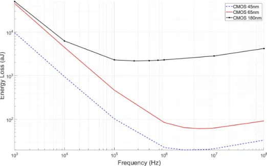
2.14 Energy dissipation per cycle as a function of the frequency for 45, 65 and 180nm CMOS node technologies. . . 27
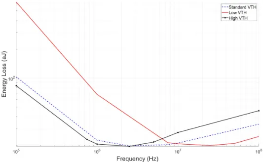
2.15 Energy dissipation per cycle as a function of the frequency for LVT, SVT and HVT MOS. . . 28
2.16 Energy dissipation per cycle as a function of the frequency for different temper-atures. . . 29
2.17 Energy dissipation per cycle as a function of the frequency for different VDDand MOS types. . . 30
2.18 Optimal energy dissipation and its associated frequency as a function of VDD.. . 31 3.1 Presentation of power delivery as (a) Mesh network, (b) tree network, (c) hybrid
network. . . 34
3.2 (a) Voltage and current of power-clock signal, (b) RC modeling of one gate and power-clock network. . . 36
3.3 Analytical equation resolution vs electrical simulation for the capacitor voltage. 39
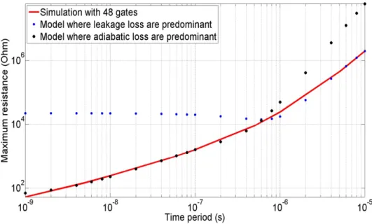
3.4 Energy loss and VHFagainst the total PCN resistance. . . 39 3.5 (a) Illustration of the vehicle adiabatic pipeline circuit of 48 stages with PFAL
buffer gates and power-clock supplies, (b) model of the power-clock network with parasitic resistance and capacitance. . . 42
3.6 Energy dissipation per cycle of a 48-stage buffer pipeline as a function of the ramp time while using adiabatic and conventional CMOS buffer gates. . . 43
3.7 Illustration of four power-clock networks represented by parasitics resistances only. . . 45
3.8 Parasitics resistance, Rmaxversus the adiabatic pipeline number of gates for
var-ious ramp times. . . 46
3.9 Maximum PCN resistance as a function of the ramp time.. . . 47
3.10 Maximum capacitance as a function of the number of gates and the model. . . . 48
3.11 Maximum PCN capacitance as a function of the interconnect parasitic resis-tance. Comparison between analytical model versus the simulation results. . . 49
3.12 Maximum capacitance as a function of the ramp time and the associated mod-els of Cl eak and Cad. . . 50
3.13 Maximum PCN resistance as a function of the ramp time. Comparison between analytical model versus the simulation results. . . 52
3.14 Maximum PCN capacitance as a function of the ramp time. Comparison be-tween analytical model versus the simulation results. . . 54
4.1 (a) Capacitive based power-clock supply, (b) ideal capacitive based power-clock signal waveform, (c) inductive based power-clock supply, (d) ideal inductive based power-clock signal waveform. . . 63
List of Figures xv
4.2 (a) The power-clock supply with the control switches and (b) model of the cir-cuit during the evaluation phase. (c) The power-clock supply with the active control switches during the hold phase and (d) its circuit model. (e) The power-clock supply with the active control switches during the recovery phase and (f ) its circuit model. (g) The power-clock supply with the active control switches
during the waiting phase and (h) its circuit model. . . 65
4.3 Illustration of a N(4k+4)-stage PFAL pipeline and its four power-clock supplies.. 67
4.4 Simulation waveforms of the power-clock signal and its control signals. . . 68
4.5 Simulation waveforms of a 4-stage PFAL pipeline and its power-clock supplies. . 69
4.6 Simulation waveforms of a 4-stage PFAL pipeline and associated power-clock supplies with unmatched inductances. . . 71
4.7 Gate resistance as a function of the Power-Clock voltage. . . 73
4.8 RMEANand RONas a function of the maximum Power-Clock voltage. . . 74
4.9 Proposed topology for a power-clock supply at nominal VDD. . . 75
4.10 Signal Waveform of a 65nm PFAL pipeline.. . . 75
4.11 Energy efficiency as a function of the width of the Pass transistor. . . 77
5.1 Layout of a PFAL buffer. . . 82
5.2 Part of the pipeline layout and its power-clock networks. . . 83
5.3 Schematic of a power-clock supply. . . 84
5.4 Layout of the integrated part of a power-clock supply. . . 85
5.5 Schematic of the control block. . . 85
5.6 Layout of one power-clock supply and its control block.. . . 86
5.7 Layout of the clock divider. . . 86
5.8 Layout of the adiabatic pipeline and its power-clock supplies. . . 87
5.9 (a) Power-clock networks in the adiabatic pipeline, (b) schematic of one power-clock network, (c) a PFAL buffer and its associated power-power-clock network para-sitics and (d) symbolic matrix representation of the connections between the PFAL buffers and the different power-clocks . . . 89
5.10 Circuit test bench. . . 90
5.11 Ideal power-clock voltages and last buffer signal voltages.. . . 91
5.12 Real power-clock voltages and last buffer signal voltages. . . 92
5.13 Model of the PFAL pipeline with its power-clock networks. . . 93
5.14 Ideal power-clock voltages and last buffer signal voltages.. . . 93
5.15 Proposed power-clock voltages and last buffer signal voltages. . . 94
6.1 Carbon Nanotube Field Effect Transistor, source: [5]. . . 100
6.2 Representation of a CNTFET with Stanford model and model parameters, source: [6]. . . 101
6.3 (a) Schematic of a PFAL CNTFET Buffer and (b) test-bench in order to quantify the energy dissipation. . . 102
6.4 Energy dissipation of PFAL CNTFET buffer as a function of the frequency for different CNTFET width values. . . 104
6.5 Energy dissipation of PFAL CNTFET buffer as a function of the frequency for different Carbon Nanotubes spacing values. . . 105
6.6 Energy dissipation of PFAL CNTFET buffer as a function of the frequency for different Carbon NanoTubes diameter values.. . . 106
6.7 Energy dissipation of PFAL CNT buffer as a function of the frequency for differ-ent CNTFET width and CNT spacing values. . . 107
6.8 Energy dissipation of PFAL buffer using CMOS or CNTFET transistors as a func-tion of the frequency. . . 108
6.9 Energy dissipation of PFAL buffer using CMOS or CNTFET transistors as a func-tion of the frequency for optimal VDD. . . 109
List of Tables
1.1 THESIS CONTRIBUTIONS . . . 11
3.1 PERCENTAGE OF DIFFERENCE BETWEEN THE ELECTRICAL SIMULATION RmaxAND THE ANALYTICAL MODEL . . . 51
3.2 PERCENTAGE OF DIFFERENCE BETWEEN THE ELECTRICAL SIMULATION CmaxAND THE ANALYTICAL MODEL . . . 51
3.3 PERCENTAGE OF DIFFERENCE BETWEEN THE ELECTRICAL SIMULATION RmaxAND THE ANALYTICAL MODEL FOR REAL-CASE APPLICATION . . . 53
3.4 PERCENTAGE OF DIFFERENCE BETWEEN THE ELECTRICAL SIMULATION CmaxAND THE ANALYTICAL MODEL FOR REAL-CASE APPLICATION . . . 53
3.5 DETERMINATION OF RmaxAND Cmax . . . 57
4.1 PASSIVE FOR POWER-CLOCK SUPPLY OF A 45NM PIPELINE . . . 67
4.2 ENERGY DISSIPATION FOR ADIABATIC PIPELINE WITH DIFFERENT
TOPOLOGIES . . . 68
4.3 ENERGY DISSIPATIONS OF THE THIRD POWER-CLOCK SUPPLY WITH DIF-FERENT INDUCTANCES . . . 71
4.4 MOS WIDTH FOR POWER-CLOCK SUPPLY OF A 65NM PIPELINE . . . 78
4.5 ENERGY DISSIPATION FOR ADIABATIC PIPELINE WITH DIFFERENT
TOPOLOGIES AT NOMINAL VDD . . . 78 5.1 ENERGY DISSIPATION OF THE DIFFERENT PIPELINES FOR DIFFERENT
POWER-CLOCK SUPPLIES . . . 92
5.2 ENERGY DISSIPATION OF THE DIFFERENT PIPELINES AND THEIR POWER-CLOCK NETWORKS FOR DIFFERENT POWER-POWER-CLOCK SUPPLIES . . . 95
C
HAPTER1
Introduction
1.1 Energy Efficiency in Integrated Circuits
1.1.1 Historical Contest
Power density has become the primary concern when a digital system is designed. As in any embedded systems, each new digital system generation has more applications than the previous one and ultimately demands more power density. This is why many re-searchers and industrial designers have been looking into novel methods for reducing power consumption of digital circuit.
Moreover, in an energy consumption point of view, with the increase numbers of Internet of Things, IoT, which are electronics devices with wireless communication, data centers and communication devices, they can represent up to 51% of the global energy demand in 2030 [2]. Fig.1.1shows the prediction of the electrical footprint in TWh of communication devices from 2010 to 2030. They are three scenarios: 1) the worst case scenario where the use of communication devices is increased and their energy efficiency stay the same, 2) the expected case scenario, where the increase of the communication devices is counter-balanced with a better energy efficiency and 3) the best case scenario, where there are less usage of communication devices and a better energy efficiency.
Figure 1.1 – Electricity footprint (TWh) of communication devices 2010-2030, source: [2].
In 2030, the expected case energy consumption of communication devices is 3.7 times lower than the worst case energy consumption. A parameter of the energy consumption increase is that more and more communication devices will be used. The other param-eter is that communication devices have more applications and denser functional block, which lead to a higher energy consumption. The integration of the functional block fol-lows Moore’s law. In 1965, Moore has predicted that the number of transistors per mm2 will doubled every two years [7].
From 1970 to the early 2000’s, doubling the number of transistor has been made by shrink-ing the dimensions of CMOS by a factor of 0.7. This is the first era of transistor scalshrink-ing, which is known as the geometrical scaling. The scaling of CMOS leads to a lower supply voltage, which leads to a lower energy dissipation per operation. However, it also leads to a higher integration and a higher operating frequency, which increase the overall power consumption [8].
1.1. ENERGY EFFICIENCY IN INTEGRATED CIRCUITS 3
Figure 1.2 – Evolution of the Intel CPU from 1970 to 2010, source: [3].
In Fig.1.2, characteristics, such as the number of transistors, the operating frequency, the power consumption and the performance, of Intel CPU are shown in a time-line. Since the early 2000’s, the operating frequency has been capped in order to limit the power con-sumption. The main blocking factor in the increase of the transistor integration is to be able to dissipate the heat coming from the energy dissipation. Heat cooling is mostly done using heat sinks, which have a fixed heat cooling density. Thus, in order to limit the circuit power dissipation density, the frequency has been capped: this is the operating frequency wall [3]. In order to continue the integration, researchers have focused their research in finding new materials to limit the transistor energy dissipation, such as high-k dielectric [9] or strained silicon [10]. These new materials reduce the effective CMOS dimension, which leads to a second era of transistor scaling: the effective scaling.
it is shown in Fig.1.2, the figure of merit of the performance, which is the power divided by the frequency, has been constant since the operating frequency was capped. In order to improve the value of such devices, the community has proposed two research axis: 1) to continue the transistor scaling ’More Moore’ and 2) the diversification of functional blocks ’More than Moore’. In Fig.1.3, the representation of the miniaturization of digital circuit is shown with respect to the miniaturization of transistors and the diversification of the func-tionalities. In order to increase the value of digital systems ’More than Moore’, researchers have developed system in package with non-digital functions, such as power management, sensing or communications [4].
Figure 1.3 – Representation of the miniaturization of the digital functions ("More Moore") and the functional diversification ("More than Moore"), source: [4]
The CMOS miniaturization has been slowed down due to the difficulty of decreasing the length of the CMOS gate for a length lower than 28nm. This difficulty comes from the dielectric. In order to create conduction in the channel, the gate should have a minimal capacitance, which is impacted by the dielectric permittivity,², surface, S and thickness, t. The capacitance is expressed as follows:
C = ²S
1.1. ENERGY EFFICIENCY IN INTEGRATED CIRCUITS 5
The permittivity depends on the dielectric, the surface is proportional to the CMOS node and the thickness has a minimal value in order to isolate the gate capacitor. Thus, with the scaling, the decrease of the surface leads to a lower capacitance value. Hence, the channel is harder to control for lower CMOS nodes. In order to continue the miniaturization of transistors, researchers have to develop new switching devices, which are known as beyond CMOS devices.
1.1.2 End of Moore’s law and research on the energy efficiency
With the emergence of beyond CMOS devices, Moore’s law has been officially ended [11]. In order to continue to increase the density of transistors in digital circuits, scientists have focus their research in four main areas: the development of beyond CMOS transistors, the diversification of functionalities, the monolithic 3D integration [12] and the development of new memories [13]. The goal is to scale one trillion of transistors by 2025 [14]. This is the third era of transistor integration: the hyper scaling. In order to improve the performance of such circuits, the energy dissipation has to be taken care of. Otherwise, the frequency will be reduced similarly to the operating frequency wall. There are 3 research axis to re-duce the energy dissipation: novel technologies and devices, new devices-, circuit- and system-level design and new architecture design style.
Beyond CMOS transistors
On novel technologies and devices level, research is axed on proposing new energy effi-cient devices such as switches like the evolution of CMOS, Carbon Nanotubes Field Effect Transistor, CNTFET, Vertical Slit Field Effect Transistor, VeSFET or Micro Electro Mechani-cal Switches, MEMS, as memories like Static Random Access Memory, SRAM. Another axis of research is the study of more energy efficient interconnections.
Following Moore’s law, bulk CMOS faces two main issues: leakage current has increased with the CMOS scaling and the gate capacitance (Eq.(1.1) is too low to control efficiently the channel known as Short Channel Effect, SCE [15]. In order to face these issues, there are two main research axes: Fully Depleted Silicon On Insulator, FDSOI and Fin Field Effect Transistor, FinFET. FDSOI is a MOSFET, which has an additional buried oxide instead of a bulk. This oxide can be polarized. This polarization is referred as the body-biasing. Thanks to this additional oxide, the capacitance, which controls the channel has a higher value. It results with a lower SCE. The second advantage of the additional oxide is the reduction of leakage [16]. The aim of FinFET is to control the channel with a 3 dimensional gate. This way, it increases the facing surface of the gate oxide and the channel, which leads to a higher gate capacitance, thus, less SCE [17]. There are two types of FinFet: bulk FinFet [18] and SOI FinFET [19].
as CNTFET does not have SCE [20]. The aim of CNTFET is to replace the doped silicon channel by Carbon Nanotubes, CNT [6]. Thus, the control of the channel resistance is easier. Another improvement of the CNTFET is that, unlike CMOS, most of the electrons are carried thanks to the ballistic transport. Ballistic transport reduces the scattering, thus the channel is less resistive and CNTFET-based logic can achieve a better performance [21]. Vertical Slit Field Effect Transistor, VeSFET is a 4 terminal FET. The novelty on this tran-sistor is that the channel is grown vertically and it is controlled by two independent gates [22]. Thanks to the two capacitances, leakage current is reduced. Due to the 4 terminals, scientists have designed novel gates, such as AND and OR functions using a single VeSFET [23].
Micro-Electro-Mechanical Switch, MEMS is a mechanical switch. Thus, the leakage cur-rent is drastically reduced. However, the performance of the switching is based on the mechanical cutting frequency of MEMS [24]. Thus, MEMS performances are lower than the performances of Field Effect Transistors, FET. Similarly to CMOS, MEMS benefits from the scaling, researchers have developed Nano-Electro-Mechanical Switch, NEMS, which have better performances than MEMS [25]. Another research axis is to develop NEMS as high ratio capacitance switch. Such devices are used in radio frequency applications or for capacitive-based logic [26].
Energy Efficient Memories
The data storage can represent up to 50% of the whole energy dissipation in electronics devices. Scientists have focused their research on reducing this energy dissipation, espe-cially the leakage dissipation. There are two types of random access memory, the Dynamic Random Access Memory and the Static Random Access Memory, SRAM. The difference between the two memory types is that DRAM needs to refresh the stored data periodically. Thus, in an energy efficiency point of view, SRAM is a better solution. However, SRAM needs more transistors in order to store one bit of data as the two SRAM cells are com-posed with 6 or 8 transistors [27]. SRAM benefits from the emergence of new technologies devices as researchers have developed SRAM using CNTFET [28] or FDSOI [29].
Energy Efficient Interconnect
Interconnect has become a main concern in high performance and low energy applica-tions. Interconnect lowers the energy efficiency and increases the signal delay. Histori-cally interconnects are made with copper [30]. With the CMOS scaling and the emergence of others FET technologies, scientist have focused their effort on improving the intercon-nects. There are two research axes: CNT based interconnects and optical interconintercon-nects. CNT based interconnects replace copper wire by carbon nanotube [31] while optical inter-connects uses light signals instead of electrical ones [32].
1.1. ENERGY EFFICIENCY IN INTEGRATED CIRCUITS 7
Energy Efficient Architecture Styles
On architecture design style, the research focuses on proposing more energy efficient ar-chitectures than Von Neumann architecture [33]. Researchers have focused their effort on optical computing, neuromorphic computing, quantum computing and probabilistic computing.
Optical computing uses optical systems to perform numerical computations [34]. The op-erations are done in the Galois Field. In order to make these opop-erations, dedicated optical gates have been designed, especially XOR gates. In addition to a higher energy efficiency, these gates have a maximal energy frequency of 7.4 THz up to now [35]. Using the designed optical gates, all-optical logic gates have been designed [36].
The aim of neuromorphic computing is to replicate how the brain computes data in order to have higher performance and a lower energy dissipation [37]. The goal of the neuromor-phic computing is to design systems with neurons, synapses and dendrites. A special ef-fort has been made on replicating synapses with electronics devices [38]. Another research area is the optimization of the architecture, i.e. where and how to place the neurons, the synapses and the dendrites [39]. Neuromorphic systems have been designed in order to highlight the performance of such systems [40].
Quantum computing relies on the quantum information theory. Thanks to this theory and proper architecture, quantum computing can achieve a better performance for a lowest energy consumption. The particularities of the quantum computing are that 1) data are stored and process thanks to quantum dots [41] 2) algorithms are needed to decipher the data stored in the quantum dots [42]. Using quantum dots, researchers have designed quantum logic [43]. The most advanced research on quantum computing has been made by IBM and its 5 Qubit quantum computer [44].
Probabilistic computing and approximate computing is a trade-off between the accuracy of the information and the energy consumption [45]. It means that the probabilistic com-puting introduces an error tolerance in order to be able to use less logic gates, a lower frequency or a lower supply voltage. Probabilistic computing relies on algorithms in or-der to optimize the system architecture with respect to the error tolerance [46]. Like the conventional computing, approximate computing benefits from the emergence of novel technology devices such as magnetic bits [47].
Energy Efficient Techniques and Design Styles
On circuit and system-level, researchers develop techniques and design style in order to reduce the energy dissipation. A common technique to lower the dynamic energy dissipa-tion is the Dynamic Voltage Frequency Scaling, DVFS [48]. DVFS adapts the supply voltage with respect to the needed frequency. As the dynamic energy dissipation is CVDD2 , reducing the supply voltage results in an energy dissipation. In order to optimize the DVFS energy
saving, researchers have rethought the power management. The most efficient manage-ment to use DVFS is the granular power managemanage-ment, i.e. each function of the circuit has its own power supply [49].
There are also alternative design styles to reduce dynamic power such as the adiabatic logic [1] or sub-threshold logic [50]. The aim of the Sub-threshold logic is to have a supply volt-age lower than the threshold voltvolt-age. Hence, CMOS operates in the weak inversion region instead of the strong inversion region. It leads to lower leakage current. The cost of such logic is that the maximal operating frequency is reduced. Sub-threshold logic reduces the leakage dissipation but also the dynamic dissipation. Indeed, similarly to DVFS, the supply voltage is reduced thus, the dynamic dissipation is also reduced [51].
Most of the power consumption of the digital circuit comes from the dynamic power - con-ventionally, the energy stored in the capacitor is dissipated twice. The essence of adiabatic logic is to charge the capacitor with a ramp then discharge the capacitor back to the sup-ply. To save energy, the charge and discharge have to be done at the lowest frequency pos-sible. Even if the adiabatic principle has been known since the 70’s, the trade-off between the power consumption and frequency was not of particular interest. With the advance-ments on novel switch technologies such as carbon nanotube field effect transistors, nano-electro-mechanical switches [52] or vertical slit field effect transistors, adiabatic logic has gained a fresh interest. Even if most of the adiabatic logic families are switch-based fam-ilies, some researchers have developed MEMS variable capacitors in order to be used in capacitive-based adiabatic logic [53].
1.2 Structure of the Thesis
This thesis focuses on the adiabatic logic. One of the particularity of the adiabatic logic is that power signal is also clock signal and it is referred as power-clock signal. The first objective of this thesis is to study how the power-clock signal can be generated and then to propose a power-clock supply topology in order to maximize the energy efficiency of adiabatic circuit.
In integrated design, one concern is the signal integrity [54]. The potential integrity is-sues come from the power delivery network and the clock delivery network. For adiabatic circuits, power delivery network and clock delivery network are combined in power-clock delivery network. The second objective of the thesis is to study how the power-clock deliv-ery network impacts the energy efficiency of the adiabatic circuit and then to propose an optimization of the power-clock delivery network.
This thesis has been funded by the French National Research Agency, ANR, with the project ADIANEMS2 (Grant number: ANR-15-CE24-0013). This project is a collaboration between ESIEE, CEA-LETI and the LIRMM. The objectives of the project is to evaluate the
poten-1.2. STRUCTURE OF THE THESIS 9
tial energy saving of an adiabatic circuit using Nano-Electro-Mechanical-Switches, NEMS. While the LIRMM objective is to develop a power-clock supply and its delivery network, ESIEE research is about designing new NEMS to be used in adiabatic logic, and the role of the CEA-LETI is to develop new design logic using these NEMSs. The thesis is organized as follows:
Chapter 2: Principle of Adiabatic Logic and its Challenges
This chapter presents the adiabatic principle, i.e. how it is possible to save energy by tuning the operating frequency. Then, we introduce the challenges of the adiabatic logic using switches. Afterwards, a state of the art on the adiabatic logic families is presented. Using this state of the art, we decide to use Positive Feedback Adiabatic Logic, PFAL, as test case for our thesis objectives. In the last part of this chapter, we present how the PFAL buffer is impacted by different parameters in order to optimize it for the test case.
Chapter 3: Study of the Power-Clock Network
In the third chapter, we study the impact of the power-clock networks, PCN, on the en-ergy efficiency of the PFAL logic. Firstly, we present a state of the art on the power-clock networks and theirs issues. Then, we study of the PCN parasitic impact on a PFAL energy dissipation. Thanks to this study, we derive constraints on the PCN parasitic in order to limit their impact. Afterwards, we investigate the impact of PCN on a circuit level and then we develop a guideline in order to optimize PCN in order to minimize the PFAL energy dissipation.
Chapter 4: Study of the Power-Clock Supply
In the fourth chapter, we study the power-clock supplies. Firstly, we present a state of the art on the power-clock supply topologies. Then, we present a power-clock supply topol-ogy in order to drive PFAL at their optimal VDD. With this topology, the power-clock
sig-nal never reaches VDDduring this evaluation, which leads to an higher energy dissipation.
Thus, we explain why and we propose the following solution to remove the additional dis-sipation. We use the proposed topology while the PFAL gates are supplied at their nominal VDD. The solution is optimized for CMOS 65nm PFAL pipeline.
Chapter 5: Design of a CMOS Adiabatic Circuit
In the fifth chapter, we present the adiabatic circuit we have designed. The adiabatic circuit is composed of a PFAL pipeline and 4 power-clocks supplies, which are designed in CMOS 65nm. The aim of this realization is to evaluate the energy saving of adiabatic circuit using our proposed power-clock supply topology and power-clock network optimization. After
we extract the PCN parasitic, we propose a model to evaluate the energy dissipation of the circuit.
Chapter 6: Adiabatic Logic Beyond CMOS
In the sixth chapter, we propose an enhancement of the positive feedback adiabatic logic. We replace CMOS by a promising field effect transistors: CNTFET. Firstly, we present a state of the art of the CNTFET. Then, we propose an optimization of theses transistors in order to have the most energy efficient PFAL gate. Afterwards, we compare PFAL CNTFET buffers with PFAL CMOS buffers in order to highlight the qualities and the drawbacks of such logic. Chapter 7: Conclusion
In the conclusion, we remind the objectives of the thesis. Then, we present the thesis con-tributions. We conclude the thesis with an opening on the current research work on the energy efficiency.
Thesis Contributions
1.2. STRUCTURE OF THE THESIS 11 Table 1.1 – THESIS CONTRIBUTIONS
Problem Proposed solution Chapter
Does the PCN has an impact on the adiabatic logic energy effi-ciency ? How can it be limited?
PCN impacts the adiabatic logic in two ways: it lowers the energy efficiency of the adiabatic logic, and it lowers the optimal operat-ing frequency. We propose a de-sign guideline to optimize PCN grids in order to limit its impact.
Chapter 3
How can the adiabatic logic be supplied at nominal VDD?
We propose a power-clock topology which can supply any adiabatic logic, which uses switches. To our knowledge, it is the first topology which includes the synchronization between each power-clock.
Chapter 4
Why is there an additional en-ergy dissipation in the power-clock proposed topology for a VDDnear threshold voltage?
The glitch is due to the pass-transistor in the PFAL buffer, we cannot model it as a constant re-sistance when VDD is not at its
nominal value. It results that an adiabatic circuit supplied by our proposed topology is more effi-cient at nominal VDD.
Chapter 4
How much energy an adiabatic circuit with the proposed topol-ogy dissipate?
We design an adiabatic pipeline, which is supplied by the pro-posed power-clocks in order to quantify the energy dissipation of such supplies. With this topology, a pipeline composed of 123952 gates dissipates 59.2pJ per cycle, which is 3 times less than a classic CMOS pipeline.
Chapter 5
The PFAL is frequency limited. Is there a solution to improve the operating frequency?
We propose to replace CMOS transistors with CNTFET in PFAL logic. This way, PFAL is more energy efficient and its optimal operating frequency increases from 2.5MHz to 400MHz.
C
HAPTER2
Principle of Adiabatic Logic and its
Challenges
In this chapter, we aim to present the adiabatic logic and its challenge with CMOS type logic. The chapter is organized as follows: in Section 2.1, we introduce the adiabatic logic. Then, in Section 2.2, we explain several challenges of using switches-based adiabatic logic. In Section 2.3, we present different adiabatic logic families. Finally, in Section 2.4, we intro-duce our most studied adiabatic logic family, the Positive Feedback Adiabatic Logic (PFAL).
2.1 Introduction of Adiabatic Logic
In this section, we introduce the principle of adiabatic logic - charging a capacitor with a ramp. Then, we explain how the adiabatic logic works.
2.1.1 Adiabatic Principle
The adiabatic switching principle is based on an efficient way to charge and discharge a ca-pacitor by using a voltage ramp [55]. For example, the energy dissipated during the charge of the gate and load capacitances, Cg at e through an active logic gate represented by its
equivalent resistance, Rg at e is as:
Echar g e=
Z T
0
Rg at ei2(t )dt (2.1)
where T is the time when the power-clock supply voltage Vφ(t ) ramps up from 0 to VDD.
The necessary requirement to maintain the adiabatic conditions is that the output voltage is equal to the power-clock supply voltage Vφ, hence ramp time T >> Rg at eCg at e[56]. Thus,
the stored charge in Cg at ewithin the adiabatic conditions is Q(t ) = Cg at eVφ(t ). In addition,
the flowing current during the ramp time is constant as i (t ) = I =∆Q∆T. Therefore, the energy dissipated during the charge time is:
Echar g e= Z T 0 Rg at ei (t )dt = Rg at eI2T = Rg at eCg at e T Cg at eV 2 DD (2.2)
Similarly, by using the same equations, the energy dissipated during the discharge time can be derived. Thus, the total energy dissipated per cycle, EALis as:
EAL= 2
Rg at eCg at e
T Cg at eV
2
DD (2.3)
There are two main schemes for adiabatic power-clock supply: resonant- and capacitive-based power supply. If the capacitor is charged by a capacitive-capacitive-based power supply, the capacitor is charged by a ramp then the energy dissipation is EAL. Else if the capacitor is
charged by a sinusoidal supply instead of a ramp, the adiabatic gate will dissipate more energy. We can accurately quantify the increase in energy dissipation by multiplying the energy dissipated by π82. Hence the adiabatic energy dissipation EADper cycle using
sinu-soidal signal is as:
EAD=π 2 4 Rg at eCg at e T Cg at eV 2 DD (2.4)
2.1.2 Adiabatic Logic
Figure 2.1 – (a) Illustration of an adiabatic logic gate with the signal and its in-verted output and (b) the representation of a four phase power-clock voltage and current.
Each adiabatic gate has as output both the function and its inverse as shown in Fig.2.1.a. Most of the adiabatic logic families use the inverted signal to maintain the output signal.
2.1. INTRODUCTION OF ADIABATIC LOGIC 15
Overall, adiabatic logic requires more signals than conventional logic. For example, in con-ventional logic, there is a power signal, clock signal, and ground, whereas in adiabatic logic there are four power-clock supply signals and ground.
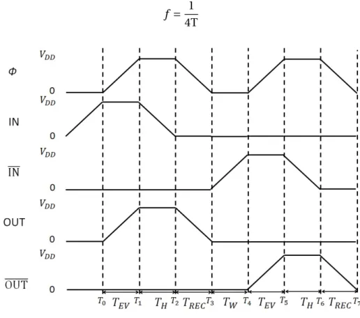
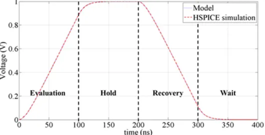
The power-clock signal which is shown in Fig.2.1.b consists of four phases: the evaluation, the hold, the recovery, and the waiting phase. In normal operating conditions, an adiabatic circuit running at the frequency f has a ramp time of T. The evaluation phase occurs between T0and T1, then the hold phase between T1 and T2. The recovery phase occurs
between T2and T3, and finally, the waiting phase is between T3and T4.
As the clock signal has 4 phases, an adiabatic circuit has to have 4 different power-clock signals. Two consecutive power-power-clocks have a 90◦phase shift. The input signal which is the output signal of the previous gate has to be in the hold phase when the power-clock signal is in the evaluation phase. Thus, in order to have the same ramp time T, each phase has the same duration then the frequency is as:
f = 1
4T (2.5)
Figure 2.2 – Representation of the different signals from an adiabatic buffer.
While the conventional logic uses voltage levels to create a logic000 or 010, the adiabatic logic is a pulse-based logic. For example, if the output signal stays at ground voltage VSS
for a whole period, then a logic000is created, whereas if the output signal is a 4-phase ramp (same as the power-clock signal) then a logic010is created also shown in Fig.2.2. Due to the presence of the output and its inverted signal, the activity factor of an adiabatic circuit is always one.
2.2 Challenges of the adiabatic logic using switches
In this section, we introduce the challenges of the adiabatic logic using switches. Most of adiabatic families are designed with CMOS or NEMS, and future switch-based adia-batic logic can be designed using CNTFET or VeSFET. Despite the chosen technology, every switch-based adiabatic logic has the same challenges: the threshold voltage or the pulling voltage for the MEMS and leakages.
2.2.1 The threshold voltage
A switch-based adiabatic logic is often composed as follow: a functional block and its com-plementary block, and two signal hold block, one for each output signal which are shown in Fig.2.3.a. Complementary inpput signal is the input of the output signal hold block and vice-versa. Then, the hold block has to be active when its input signal is ’0’. For example, the hold block can be a PMOS for CMOS based adiabatic logic.
During the recovery phase, the two input signals are at the waiting phase. It means that we can not rely on the functional block to ensure a conduction path between the output and the power-clock. Thus, the recovery is going through the hold block, in our example a PMOS.
Figure 2.3 – (a) Switch-based adiabatic logic, and (b) representation of the power-clock and output signals.
2.2. CHALLENGES OF THE ADIABATIC LOGIC USING SWITCHES 17
Every switch has a threshold voltage, to distinguish off- and on-state. As the hold block is active when its input is ’0’, the output signal is passing when its voltage is between VTHand
VDD. It means that during the recovery phase, there is a conduction path between
power-clock and output as long as the power-power-clock signal is higher than VTH. Thus, the stored
energy in the output can not be fully recovered. In Fig.2.3.b, the output signal is shown with respect to VTH. Moreover, the stored energy, which has not been recovered during the
recovery phase is lost at the next evaluation phase. Thus, we define the energy dissipation due to the threshold voltage, ETHas:
ETH=
1 2CV
2
TH (2.6)
As this threshold effect is not dependent of the ramp time, using Eq.(2.3) and Eq.(2.6), the minimum energy dissipation per cycle of a switch-based adiabatic logic is the threshold dissipation.
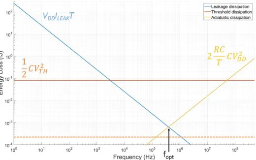
2.2.2 Adiabatic logic principle vs leakages
As we introduced in the previous subsection, the threshold voltage causes a non-adiabatic loss. Thus, we could consider to reduce VTHin order to increase the recovered energy.
How-ever, the threshold voltage is one key parameter of the switch leakages. Energy dissipation per cycle coming from the leakages is expressed as:
ELeak= VDDILeakT (2.7)
where ILeakis the gate leakage current.
The total energy dissipation coming from an adiabatic circuit is expressed as:
ETot= EAL+ ETH+ ELeak (2.8)
When VTHincreases, Il eak is decreasing. Thus, there is a trade-off between VTHand ILeak.
Fig.2.4shows the different types of energy dissipation as a function of the operating fre-quency defined in Eq.2.5. As ELeak is inversely proportional to the frequency, f, and EALis
proportional to f , there is an optimal frequency fopt where the leakage and the adiabatic
dissipation are equivalent. There are two cases: 1) The threshold dissipation is lower than the leakage dissipation at the optimal frequency, thus fop t is also the optimal frequency of
the gate. 2) The threshold dissipation is higher than the leakage dissipation, thus there is a range of frequencies, where the threshold dissipation is predominant, which are the op-timal frequencies of the gate. In order to highlight these two cases, the energy dissipation shown in Fig.2.4has been done with a gate resistance of 10kΩ and capacitance of 1f F, a supply voltage of 1V and two threshold voltages: 0.3V and 0.6V.
Figure 2.4 – Asymptotic representation of the different energy dissipation coming from an adiabatic logic gate as a function of the operating frequency.
In conclusion, the best switch for switch-based adiabatic logic is a switch with a low VTH
VDD in order to recover most of the energy, which is stored in the gates, and with no leakage in order to reach the lowest energy dissipation ETH.
2.3. ADIABATIC LOGIC FAMILIES 19
2.3 Adiabatic logic families
In this section, 7 different adiabatic logic families are presented. These logics are repre-sentative of the different types of adiabatic logic. Each of these families are considered as quasi-adiabatic logic families i.e. the energy stored in the gate cannot be fully recovered due to the threshold voltage effect during the recovery phase. We could also present full-adiabatic logic families which can fully recover the energy during the recovery phase. How-ever, due to the complexity of their implementation, these families have not been taken into consideration as a load for the power-clock study.
2.3.1 Positive Feedback Adiabatic Logic
Positive Feedback Adiabatic Logic, PFAL, is one of the most widely used adiabatic logic family [57,58]. It is supplied by a 4-phase ramp power-clock. Thus, the frequency is as defined in Eq.(2.5).
Figure 2.5 – (a) PFAL buffer, and (b) representation of the power-clock and output signals.
In Fig.2.5.a, a PFAL buffer is shown. The functional block is in parallel with a PMOS, which ensures the hold phase. Each PMOS are driven by the other output signal i.eout put drives
the PMOS connected to the output and vice versa. The role of the NMOS connected to VSS
is to discharge the energy which has not been recovered during the evaluation phase. In Fig.2.5.b, power-clock and output signals are shown. If the buffer input is ’1’, then the output copies the power-clock. Else, the output remains at VSS.
PFAL logic costs more area than classic logic. Indeed, hold block are composed of 4 sistors, it needs the same number of transistors to create the function, plus additional tran-sistors for the complementary function.
2.3.2 Clocked Adiabatic Logic
Clocked Adiabatic Logic, CAL, is a 4-phase power-clock adiabatic family where the gates can be disconnected from the power-clock [59]. As the activity factor of an adiabatic gate is always 1, disconnecting the not-needed gate will decrease the adiabatic energy dissipation and the threshold dissipation.
Figure 2.6 – (a) CAL buffer, and (b) representation of the power-clock and output signals.
In Fig.2.6.a, a CAL buffer is shown. There is an additional signal CX which connects the functional blocks. The main difference with PFAL is that the functional block connects the complementary output to VSSinstead of connecting the output to the power-clock.
In Fig.2.6.b, power-clock, CX and output signals are shown. If CX is ’0’, then output and
out put remain at VSS. Else, it acts as a PFAL buffer.
CAL logic costs more area than PFAL logic due to the two additional NMOS needed to dis-connect the gate. Moreover, CX signal is not an adiabatic signal, thus, the energy dissipa-tion to charge and discharge CX NMOS is CVDD2 : disconnecting gates too frequently might not save energy.
2.3.3 Two Phase Adiabatic Static Clock Logic
Two Phase Adiabatic Static Clock Logic, 2PASCL, is a two-phase power-clock adiabatic logic family [60]. It has two main advantages: as a two-phase power-clock family, for the same adiabatic dissipation Eq.(2.3), the frequency doubles; and the complementary input is not needed, i.e. the activity factor could not be 1.
In order to have a two-phase power-clock adiabatic logic without complementary signal, each gate needs two different power-clock signals (Fig.2.7), a positive power-clock which
2.3. ADIABATIC LOGIC FAMILIES 21
voltage is betweenVDD
2 and VDD, and a negative power-clock which voltage is between VDD
2
and VSS. The next gate positive (or negative) power-clock has a 180◦ phase shift with the
positive (resp. negative) power-clock. In total, there are 4 different power-clocks.
Figure 2.7 – (a) 2PASCL inverter, and (b) representation of the power-clock and output signals.
In Fig.2.7.a, a 2PASCL inverter is shown. There are the functional block and two additional hold signal MOS which are connected to the different power-clock.
In Fig.2.7.b, power-clock and output signals are shown. If the input is ’0’, then the output copies the positive power-clock, else it remains at VSS. As the signal is recovered only from
VDDto VDD2 every time the input changes, there is a non-adiabatic dissipation of 18CVDD2 . It
means that for high activity factor, 2PASCL can dissipate more energy than PFAL or CAL. As there is no complementary signal, 2PASCL costs less area than the two previous fami-lies but it is also more sensitive to the noise coming from the inputs signals and the two different power clocks.
2.3.4 Pass-transistor Adiabatic Logic
Pass-transistor Adiabatic Logic, PAL, is a two-phase power-clock adiabatic family [61]. In Fig.2.8.a, a PAL buffer is shown. There are the functional and its complementary func-tional blocks and two hold signal PMOS. The difference with a PFAL logic is that there are no NMOS to discharge the outputs, instead there are two power-clocks. The positive clock which is used to charge and discharge the outputs and the negative power-clock which is used to fully discharge the outputs.
next gate power-clock is the negative (resp. positive) current gate power-clock. A PAL cir-cuit has only 2 power-clocks.
Figure 2.8 – (a) PAL buffer, and (b) representation of the power-clock and output signals.
In Fig.2.8.b, power-clock and output signals are shown. If the input is ’0’, then the output remains at VSS, else, the input copies the positive power-clock.
PAL logic costs less area than PFAL logic but as it has two different power-clock signals and no hold phase, the noise sensitivity is increased.
2.3.5 Latched Pass-transistor Adiabatic Logic
Latched Pass-transistor Adiabatic Logic, LPAL, is a two-phase power-clock adiabatic family [59] where the gate can be disabled. It is the equivalent of the CAL family for the PAL. In Fig.2.9.a, a LPAL buffer is shown. It is the architecture of a PAL buffer plus one NMOS and one PMOS. The aim of these additional MOS is to connect or disconnect the gate to the power-clocks. Two more signal mode and mod e are needed to drive these MOS. In Fig.2.8.b, power-clock and output signals are shown. If mode is ’1’, the LPAL buffer acts as a PAL buffer. Else, the output are idle. It means that the output voltages will stay at VDD
or VSSuntil the gate is reconnected.
LPAL gate costs more area than a PAL gate and the same area as a PFAL gate due to the two extra MOS. As the CAL, mode andmod e are not adiabatic signals which mean that every
2.3. ADIABATIC LOGIC FAMILIES 23
Figure 2.9 – (a) LPAL buffer, and (b) representation of the power-clock and output signals.
2.3.6 Single Rail Adiabatic Dynamic Logic
Single Rail Adiabatic Dynamic Logic, SRADL, is a 4-phase NEMS-based adiabatic logic fam-ily [52]. The 4 phases differ from the CMOS-based adiabatic families. The evaluation phase is a pre-charge phase, it charges the output if needed. The hold phase is still a hold phase, the output signal remains at VDD while the input is transitioning. The recovery phase is
an evaluation phase, the input is evaluated while the power-clock is ramping down. The waiting phase is an idle phase, the output is maintained. As the 4 phases are different, the state ’0’ and ’1’ are also different. A ’0’ (resp. ’1’) state is when the idle phase is at VDD(resp.
VSS).
In Fig.2.10.a, a SRADL inverter is shown. It is composed of one NEMS. Output signal is held thanks to the second electrode of the NEMS. In order to hold the signal, a bias voltage, VB,
has to be applied to this electrode.
In Fig.2.10.b, power-clock and output signals are shown. If the input is ’1’, the output volt-age should be at VDD. Then, if the previous input was ’1’, the output is already at VDD, thus
there is no charging during the evaluation phase. Else, the output signal ramps up to VDD.
If the input is ’0’, the output should copy the power-clock. However, if the previous state was ’1’, the output is non-adiabatically discharged before copying the power-clock.