HAL Id: hal-00166761
https://hal.archives-ouvertes.fr/hal-00166761
Submitted on 9 Aug 2007
HAL is a multi-disciplinary open access
archive for the deposit and dissemination of
sci-entific research documents, whether they are
pub-lished or not. The documents may come from
teaching and research institutions in France or
L’archive ouverte pluridisciplinaire HAL, est
destinée au dépôt et à la diffusion de documents
scientifiques de niveau recherche, publiés ou non,
émanant des établissements d’enseignement et de
recherche français ou étrangers, des laboratoires
Dispersion Impact on Ballistic CNTFET n+-i-n+
Performances
Patricia Desgreys, J. Gomes da Silva, D. Robert
To cite this version:
Patricia Desgreys, J. Gomes da Silva, D. Robert. Dispersion Impact on Ballistic CNTFET n+-i-n+
Performances. ENS 2006, Dec 2006, Paris, France. pp.37-42. �hal-00166761�
DISPERSION IMPACT ON BALLISTIC CNTFET N+-I-N+ PERFORMANCES
Patricia Desgreys, Jefferson Gomes Da Silva, Dorothée Robert
LTCI – CNRS 5818 – GET-Télécom Paris
46 rue Barrault
75634 Paris Cedex 13 - France
ABSTRACT
The designs integrating the promising carbon nanotube transistors (CNTFET) will have to take into account the constraints implied by the strong dispersion inherent to nanotube manufacturing. This paper proposes to characterize the main CNTFET performances: on-current Ion, Ion/Ioff ratio and inverse sub-threshold slope S
according to the dispersion on the nanotube diameter. For this purpose, we use a compact model suitable for testing several diameter values.
1. INTRODUCTION
The carbon nanotubes belong to the fullerenes family which is a carbon allotropic variety. Since their discovery in 1985, their remarkable structure and their properties have been studied and recently, carbon nanotube field effect transistors have attracted a great deal of attention as possible building blocks of a future nanoelectronics due to their unique structural and electronic properties.
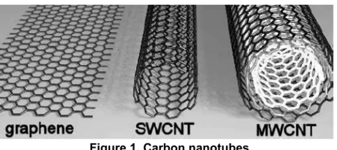
Figure 1. Carbon nanotubes.
A carbon nanotube can be seen like a graphite sheet rolled up on itself with a diameter typically between 1 and 5 nm. The nanotube can be a metal or a semiconductor according to its chirality, characterized by the chirality vector (n, m). Because only semiconductor nanotubes are appropriate for transistors implementation, we initially consider semiconductors single walled nanotubes obtained by free growth. The assumed chirality is often the zigzag one (n, 0) which ensures the semiconductor character provided that n is not a multiple of three. It results from
this geometry a strong 1D quantum confinement around the circular direction of the tube which takes part in the good electronic properties of the nanotubes: high carrier mobility, low leakage current, important on state current relatively to the applied voltages and low inverse sub-threshold slope. These properties allow us to consider the design of high-speed and high performances electronic circuits.
The manufacturing processes progress continually: one of the most advanced is the Chemical Vapor Deposition technique (CVD). However, there is still a strong spreading on the obtained diameters and the control or the selection of the diameters and/or the chiralities remain complex operations. Finally small semiconductors nanotubes are easier to manufacture with accuracy.
Figure 2. CNTFET geometry and key parameters.
The central part of a CNTFET is an intrinsic (i) semiconductor tube surrounded with or posed on a combination insulator plus gate; this assembly does not have specific n or p behavior but presents a total ambivalent behavior according to the voltage applied to the gate. The three key parameters which govern the CNTFET operation are:
• the length: we consider low length tubes (L<15nm) so that transport in the nanotube is ballistic that corresponds to the statistical absence of collisions and thus to the maximum carrier speed.
• the diameter : the current delivered by the transistor according to the voltages which are applied to it strongly depends on the nanotube’s diameter which fixes the energy of the bandgap Eg and the number of the implied sub-bands.
• the nature of the contacts at each extremity of the intrinsic tube: the current is controlled by the
L d h Grille ZrO2 ZrO2 Grille L d h
Authors
Title. Cut at approx. 70 characters if it is too long....
transmission of the carriers through the contacts. The two types mostly considered, are schottky contacts metal-i-metal and doped nanotubes n+-i-n+; in principle, the second one exhibits superior device characteristics (better off state and better on state) [1] ,[2].
Now, the improvement of the CNTFET must be coupled with the development of circuit compatible models so that the possibilities of these new components can be explored at the system level. In this context, we present our work on compact modeling and simulation of the ballistic CNTFET for several diameters. This model will allow to test electronic architectures taking into account component dispersion.
Part 2 details the compact model used and our contribution to the widening of this model to any value of d ranging between 1 and 5 nm. Part 3 shows simulation results obtained from a MATLAB implementation of this model and part 4 studies the impact of diameter, carbon-carbon bonding energy and oxide dielectric constant dispersions on the transistor static performances.
2. MODEL PRESENTATION 2.1. 1D ballistic model
Ballistic doped drain/source CNTFET operates like a conventional MOSFET with a barrier height modulation and there is no tunnelling barrier. Its physical structure is an intrinsic CNT with n+ doped nanotubes as a source and drain. A coaxial gate is placed around the intrinsic part of the nanotube and separated by an oxide. The model exposed here is in a large part extracted from the paper [3]. It is based on the works of the most advanced research group with Datta and Lundstrom from Purdue University and this model is close to underlying physics.
The gate voltage VG induces charge QCNT and
potential ΨS in the CNTFET channel. It also modulates
the top barrier of the energy band between the source and the drain. As the source-drain barrier is lowered, current flows between the source and the drain. For ballistic transport, all scattering mechanisms can be neglected. The current will remain constant throughout the channel and we may compute it at the top of the energy band, at the channel beginning.
2.2. Model equations
The relation between ΨS and VG is given by:
S S ( ) ( ) CNT S G G Sp Dp p INS INS Q e V V n n C C ψ = − = − ⋅
∑
ψ + ψ (1) nSp and nDp are the carrier’s densities in the sub-bandp and coming respectively from the source and the drain.
The calculation of these quantities requires the knowledge of the potential ΨS. 0 ( , ) , S p i ip p i b n N F i S D i K T ψ µ ξ ξ − ∆ − = ∆ = = (2)
∆p is the energy of the bottom of the sub-band p
conduction band. 0 2 2 0 ( , ) 1 exp( ) b N F x y dz z y y x K T +∞ = + − + − ⋅
∫
(3) 2 2 ( p) p z= E+ ∆ − ∆ 0 4 3 b K T N V b π Π = (4)VΠ is the carbon-carbon bonding energy and b the
C-C bonding distance. Then, the knowledge of the potential ΨS allows the calculation of the drain source current
according to the Landauer formula:
[
]
4 ln(1 exp( )) ln(1 exp( )) b DS s D p eK T I h ξ ξ =∑
+ − + (5)The difficulty is that the equations (1) and (2) must be self consistently solved. However F(x, y) does not have an analytical solution. A possibility is then to approach this equation by the two following functions (valid for ∆p <0.5 eV): 0 2 exp( ), fo 0 = , f 0 5.3 p 10 p 1 0.34 p 1 n A r N B C or with A C and B ξ ξ ξ ξ = < + ≥ = = − ∆ + ∆ + = ∆ + (6)
With this approach, we can numerically solve the model equations set and find a relation between VG and
ΨS. In this resolution, the nanotube’s diameter d is implied
in the calculation of the bottom energy of the first conduction sub-band ∆1 (7), in the determination of the
number of sub-bands necessary for the current calculation (8) and in the expression of the insulator capacity CINS (9)
or (10). 1 0.43 [ ] V b d d nm Π⋅ ∆ = = (= Eg/2) (7)
( )
1 6 3 1 4 p p p − − −∆ = ∆ (in the vicinity of EF) (8)
If the nanotube is posed on an oxide plane of height h, of permittivity εox, the capacity per length unit is
expressed by [4]:
(
0)
2 ln 2 2 / ox INS C h d d πε ε = + (9)If the intrinsic nanotube is surrounded by a coaxial gate, both separated by an oxide of thickness h, the gate influence is more important (traditional cylindrical structure):
(
0)
2 ln 2 / ox INS C h d d πε ε = + (10)The equations were solved in a particular case of diameter and value of insulator capacitance. The results extracted from [3] and reported in figure 3, show that there is an empirical approximate relation between potential VG and ΨS: GS 1 GS 1 GS 1 0, pour V (V - ), pour V GS S V ψ α − = < ∆ = ∆ ≥ ∆ (11) 2 0 1VDS 2VDS α α= +α +α (12)
Figure 3. VG-ΨS in function of VG for two values of VDS for
d=3nm and CINS=17 pF/cm [3].
This approximation is interesting because it allows to quickly calculate the current in the transistor starting from the voltages applied to the gate and the drain (by taking the source as reference) and the data of the three empirical parameters α0, α1 and α2.
2.3. Automatic determination of parameters α
αα
α0, αααα1 and αααα2
From there, our work focused on the development of a MATLAB program implementing the automatic calculation of the values α0, α1 and α2. The program
CMVD (Compact Model for Variable Diameter) inputs are the transistor geometry, the oxide nature and thickness and it delivers α0, α1 and α2 in function of d in the range
from 1 to 5 nm. The MATLAB program solves the equations for a vector of VGS values and for three values
of VDS. Initially, a great number of VGS were considered
and α was the slope of least squares straight line. This phase of analysis allow to check that the linear behaviour was well observed as on figure 3 for other values of d and CINS. So we simplified the program considering only two
values of VGS for the determination of α : VGS =0 and VGS
=0.8V. The set of values obtained can be introduced into a compact model of ballistic transistor CNTFET n+-i-n+ implementing the equations (2), (5), (7), (8), (11) and (12). We can thus quickly perform simulations for several values of the diameter and study the impact of dispersion on the first architectures based on CNTFET.
Figure 4 shows the values obtained for a coaxial grid with h=3nm and εox=25. The values of these parameters
alpha are the results of numerical approximations: they do not have any physical meaning and this explains their abrupt variations. At this stage, a polynomial approach to obtain relations α0(d), α1(d), and α2(d), can’t be done with
accuracy. Thus either the main program of CNTFET-based circuit simulation calculates itself the alpha values or they are provided by tables in a circuit simulator.
Figure 4. αααα0, αααα1 and αααα2 in function of d for a coaxial gate
with h= 3 nm and εεεεox =25 (εεεεox = 18 – 40 for ZrO2).
Figure 5. IDS in function of VDS for d=1nm, h=2nm and
εεεεox=25 (a) Physical simulation results (b) Matlab CMVD
simulations. (b)
Authors
Title. Cut at approx. 70 characters if it is too long....
3. SIMULATION RESULTS
In this part, we present our first simulation results of the static characteristics for the ballistic transistor CNTFET n+-i-n+. These characteristics are obtained with our program in MATLAB. The aim is to compare them with the curves available in the literature. The publications of measurement results on CNTFET n+-i-n+ structures are nearly non-existent and the curves found in the literature are rather the results of numerical simulations from physical equations (1D Poisson equation and Schrodinger equation are self consistently solved).
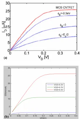
3.1. Simulation Id(VD) for VG=0.4V with d=1nm
The curves shown in figure 5(a) are extracted from the article [1] whose aim is to show that MOS like CNTFET has better performances than SB CNTFET. A CMVD Matlab simulation was done with the same assumptions: coaxial gate with h=2nm, εox=25 and d=1nm. Results are
reported in figure 5(b) and we note a good accordance between the two curves concerning the MOS like CNTFET with VGS=0.4V above conduction threshold.
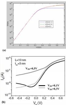
3.2. Simulation for d=1.4nm, h=3nm and εεεεox =25
Figure 6. IDS in function of VGS for d=1.4nm, h=3nm and
εεεεox=25 (a) Matlab CMVD simulations (b) Physical simulation
results.
The curves of the figure 6(b) are extracted from [2] and they are the results of numerical simulations from physical equations. We compare to CMVD Matlab simulation, figure 6(a), obtained in the same bias conditions and with the same assumptions on geometry. For VDS equal to 0.1V or 0.3V and VGS>0, the curves are
comparable. But our model seems to give better performances:
Parameter\Model CMVD Physical Current Ion several 10µA 10 µA
Inverse sub-threshold slope S
60 mV/dec 100 mV/dec
Tableau 1. Performances obtained with two types of modelling.
The performances obtained with the compact model correspond to a highest limit of the totally ballistic CNTFET. In particular, the compact model does not take into account the length of the nanotube. For VDS=0.5V,
the curves don’t match because there is another phenomenon not taken into account in our model. There is a flux of holes from the drain due to band to band tunneling (BTBT) and the off state is degraded.
4. DISPERSION IMPACT
4.1. Dispersion due to the diameter variations When the CNTFETs are manufactured, there is a great dispersion on the obtained diameters. For example, for a required diameter of 1.4 nm, we obtain a collection of nanotubes between 1.2 and 1.6 nm. The object of this part is to characterize resulting dispersion on the main characteristics of the CNTFET. The currents at the one and off state correspond respectively to VGS=0.7V and
VGS=0.1V, the inverse sub-threshold slope S is the
minimal inverse slope observed.
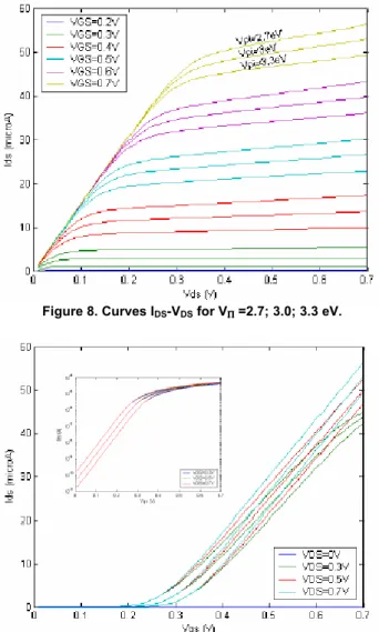
Figure 7. IDS in function of VGS for d=1.2nm, 1.4nm and
1.6nm, h=3nm and εεεεox=25.
VDS=0,1V
VDS=0,3V
VDS=0,5V
According to the results shown on figure 7, we note that the sub-threshold slope is not modified by a diameter spreading. On the other hand, the current levels change: numerical values are reported on table 2. It shows that there is a limited dispersion on the Ion current of
approximately 10%; on the other hand, the Ion/Ioff ratio is
very sensitive to diameter spreading with a factor 30 between the minimal value and the maximum value.
Parameter\diam. 1.2nm 1.4nm 1.6nm Current Ion 37µA 42µA 45µA
Ratio Ion/Ioff 379.10 3
55.103 12.103 Tableau 2. Simulated performances for several diameter values for VDS=0.3V.
A compromise should be found between the different required performances: a small diameter leads to a low off-state current and a high Ion/Ioff ratio while a large
diameter leads to a high on-state current. And it is however difficult to control the diameter of the nanotube at the time of its manufacture in order to obtain the optimal value of 1.4nm.
Others physical parameters values vary in a wide range when nanotubes are manufactured. In the two following parts, we propose to study the impact of the variations of the Carbon-Carbon (C-C) bonding energy VΠ and of the oxide dielectric constant εεεεox. The studied
transistor has the following characteristics:
• nanotube diameter of 1.4nm corresponding to the chirality (15;5)
• coaxial geometry: the nanotube is surrounded by the gate
• gate oxide thickness of 3 nm
• oxide dielectric constant of 25 (plus or minus 10) • C-C bonding energy of 3eV (plus or minus
0.3eV)
4.2. Dispersion due to the C-C bonding energy
C-C bonding energy depends, amongst others things, of nanotube geometry, of temperature and also of the possible topological defects. For example, the network of hexagons can contain pentagon-heptagon pairs leading to changes of the nanotube diameter and of the electronic behaviour around the Fermi level.
So we studied the impact of VΠ variations around
3eV. We plotted IDS-VGS and IDS-VDS curves for several
values of VΠ and we determinated resulting variations on
static performances of CNTFET.
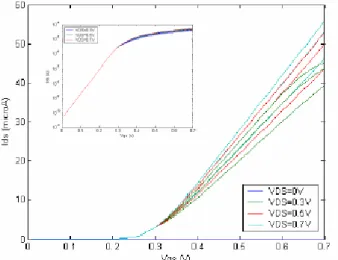
As seen in the figures 8, 9 and 10, the static performances are modified: the on current decreases by 1.1 and the off current decreases by a factor 10 when VΠ
increases from 2.7 to 3.3 eV, which induces threshold
voltage and ION/IOFF ratio increases. This last is multiplied
by 8 when VΠ moves from 2.7eV to 3.3 eV.
Figure 8. Curves IDS-VDS for VΠΠΠΠ =2.7; 3.0; 3.3 eV.
Figure 9. Curves IDS-VGS for VΠΠΠΠ =2.7; 3.0; 3.3 eV with linear scale and logarithmic scale in the inset.
Authors
Title. Cut at approx. 70 characters if it is too long....
4.3. Dispersion due to the oxide dielectric constant An oxide often used in the transistors for its great relative permittivity is the zirconium oxide also called zircon (ZrO2). Its permittivity can vary to a significant degree, between 15 and 35. By studying dispersion using a Matlab routine, one obtains the following curves:
Figure 11. Curves IDS-VDS for εεεεr =15; 25; 35.
On these curves giving IDS in function of VDS, one
realizes that the on current increases with εr. At VDS = 0,5
V and VGS = 0,7 V, for εr varying from 15 to 35, the
current ION moves from 44 µA to 53 µA, that represents an
increase of approximately 20 %.
Figure 12. Curves IDS-VGS for εεεεr =15; 25; 35 with linear scale
and logarithmic scale in the inset.
The curves IDS in function of VGS in logarithmic scale
show that the off current and the inverse sub-threshold slope are not modified. The linear scale show the current fluctuations at the on state previously noted, and the voltage threshold does not vary.
5. CONCLUSIONS
The compact modelling of the ballistic CNTFET whose source and drain are in doped nanotube is interesting because it corresponds to the most powerful transistor with nanotube. The model, based on a surface potential integration, is already exploitable provided that its validity range is well defined. In particular, the model is valid for low applied voltages VG in order to not populate the
sub-bands of energy higher than 0.5eV. We added in our model implementation a module of automatic calculation for the parameters α0, α1 and α2 depending on the
nanotube diameter in order to study the influence of dispersions on the CNTFET performances. The continuation of our work will both address the model improvement: extension of the validity field for the static model and addition of the dynamic behaviour [5] and the study of the dispersion influence on analogical and mixed architectures.
6. ACKNOWLEDGEMENT
The authors thank the partners of project NANOSYS: http://nanosys.ief.u-psud.fr/
This project is financed by the CNRS within the framework of an Inciting Joint Action Nanosciences.
7. REFERENCES
[1] J. Guo, A. Javey, H. Dai, S.Datta et M. Lundstrom, "Predicted Performance Advantages of Carbon Nanotube Transistors with Doped Nanotubes as Source/Drain", eprint ARXIV:cond-mat/0309039, Sept. 2003.
[2] J. Knoch, S. Mantl et J. Appenzeller, "Comparison of transport properties in carbon nanotube field-effect transistors with Schottky contacts and doped source/drain contacts", Solid-State Electronics available online at www.sciencedirect.com, Aug. 2004.
[3] A. Raychowdhury, S. Mukhopadhyay et K. Roy, "A circuit-compatible model of ballistic carbon nanotube field effect transistors", IEEE Trans. on Computer-Aided Design of ICS, vol. 23, n°10, Oct. 2004.
[4] P. Avouris, R. Martel, V. Derycke et J. Appenzeller, "Carbon Nanotube Transistors and Logic Circuits ", Physica B, vol. 323, p. 6-14, 2002.
[5] S. Hasan, S. Salahuddin, M. Vaidyanathan et M. A. Alam, "High-frequency Performance Projections for ballistic Carbon-Nanotube Transistors", IEEE Trans. on Nanotech., vol. 5, no 1, January 2006