O
pen
A
rchive
T
OULOUSE
A
rchive
O
uverte (
OATAO
)
OATAO is an open access repository that collects the work of Toulouse researchers and
makes it freely available over the web where possible.
This is an author-deposited version published in :
http://oatao.univ-toulouse.fr/
Eprints ID : 17326
To link to this article : DOI : 10.1038/srep37699
URL :
http://dx.doi.org/10.1038/srep37699
To cite this version :
Kumar, Sunil and Maury, Francis and
Bahlawane, Naoufal Electrical Switching in Semiconductor-Metal
Self-Assembled VO2 Disordered Metamaterial Coatings. (2016)
Scientific Reports, vol. 6. pp. 37699.
Any correspondence concerning this service should be sent to the repository
administrator:
[email protected]
Electrical Switching in
Semiconductor-Metal
Self-Assembled VO
!
Disordered
Metamaterial Coatings
Sunil Kumar", Francis Maury! & Naoufal Bahlawane"
As a strongly correlated metal oxide, VO! inspires several highly technological applications. The challenging reliable wafer-scale synthesis of high quality polycrystalline VO! coatings is demonstrated #$%&'%()%*+,)$-%+./+$*+-0%#1%*20%#3).+*)/0%4)$*05)$-%#1%6207)6+889%/+:#5%.0:#4)*0.%;<!%=874>%?2)4% +::5#+62%504@8*4%)$%=874%A)*2%+%407)6#$.@6*#5B70*+8%*5+$4)*)#$%C(D?E%F@+8)*9%+::5#+62)$-%*2+*%#1%*20% epitaxial counterpart. SMT occurs with an abrupt electrical resistivity change exceeding three orders of magnitude with a narrow hysteresis width. Spatially resolved infrared and Raman analyses evidence the self-assembly of VO!%.)4#5.050.%70*+7+*05)+8G%6#7:504)$-%7#$#68)$)6%CD"%+$.%D!E%+$.%5@*)80%CHE% .#7+)$4G%+*%*20%*5+$4)*)#$%*07:05+*@50%50-)#$>%?20%D!%70.)+*)#$%#1%*20%D"BH%*5+$4)*)#$%)4%4:+*)+889% 6#$=$0.%+$.%508+*0.%*#%*20%8#6+8)I0.%4*5+)$B4*+J)8)I+*)#$%#1%*20%D!%:2+40>%?20%:5040$60%#1%*20%D!%:2+40% is supposed to play a role as a minor semiconducting phase far above the SMT temperature. In terms of application, we show that the VO! disordered self-assembly of M and R phases is highly stable and can be thermally triggered with high precision using short heating or cooling pulses with adjusted strengths. Such a control enables an accurate and tunable thermal control of the electrical switching.
The property of exhibiting phase transitions in strongly correlated metal oxides has opened up new applica-tion possibilities. Vanadium dioxide (VO2) has seen a particular interest owing to its Semiconductor to Metal
Transition (SMT) occurring at a temperature (Tc) of 67 °C1. VO2 undergoes a first order phase transition from a
highly resistive semiconducting monoclinic (M1) phase to a metallic rutile (R) phase with an effective change of electrical resistivity of 3–4 orders of magnitude within a narrow range of temperature2–4. This change in electrical
properties is accompanied by a remarkable optical transition, where the material shows thermochromic behavior in the infrared (IR) region. VO2 effectively reflects the IR radiation in the high temperature rutile phase while
being IR transparent at the low temperature monoclinic phase5–8. Such unique combination of properties marks
it as a crucial material of study not only for developing intelligent thermal, resistive and optical switches9–15, but
also from the fundamental point of view.
Obtaining high quality VO2 films, essential for high technological applications, remains a challenge as
vana-dium forms multiple stable oxides like V2O3, V2O5 and V6O1316. Hence, it is crucial to control the growth
condi-tions to a high degree of precision to obtain pure single-phase films. Polycrystalline and epitaxial films have been grown by various deposition techniques including Sol gel17, Pulsed Laser Deposition (PLD)4, Molecular Beam
Epitaxy (MBE)18, Atomic Layer Deposition (ALD)19, Sputtering20, and Chemical Vapor Deposition (CVD)21–23.
Epitaxial films grow on pre-treated and appropriately oriented Al2O3 or TiO2 substrates or buffer layers24–26. The
SMT-relevant indicators of the VO2 films quality are the amplitude of resistivity change and hysteresis width.
Ideally, VO2 films show 3–4 orders of magnitude resistivity change with a narrow hysteresis width of ∆ T~ 3–4 K.
Bulk single crystal offers slightly higher amplitude of resistivity change but is susceptible to breakdown after few cycles of switching between semiconducting and metallic phases27. Although, polycrystalline thin films
with-stand frequent cycling, they usually feature broad hysteresis and small amplitudes of resistivity change, due to the presence of high density of grain boundaries and grain-boundary defects23,28,29. Sintering as-grown VO
2 films to
decrease the density of grain boundaries is not conceivable for practical applications due to the high melting point
!"#$%&'(#)*+,-./0/#/%+(1+230%-3%+4-5+6%37-(8(*9+:",26;<+=+4>%-#%+5%.+?4#/.@A(#)-%4#$+"@BCDE+F.37@.#)@G8H%//%+
Luxembourg. EI,J,KG6<+FL2,GIF6@B+488M%+FN+K(-.(<+C!OCO+6(#8(#.%<+A)4-3%N+I())%.P(-5%-3%+4-5+)%Q#%./.+1()+
of this phase (1970 °C). The depression of the melting point, usually observed in nano-crystalline materials30 is
unlikely to reduce the sintering temperature to a reasonable range. Epitaxial VO2 films attracted a considerable
attention owing to their improved morphological advantages and SMT quality. Nevertheless, cost, process condi-tions, ease of synthesis, morphological control and industrial integration remain limiting challenges for epitaxial growth of VO2. Hence, it is worth investigating ways to grow polycrystalline VO2 films without specific buffer
layers, yet still matching the performance of epitaxial or single crystal VO2.
The synthesis of high quality, electronic grade, wafer-scale VO2 films by MOCVD is achieved involving an
oxidative sintering step. The investigation of the electrical and optical properties across the SMT reveals the self-assembly of a VO2–disordered metamaterial in which the coalescence and confinement of metallic domains
are highly controllable.
Results and Discussion
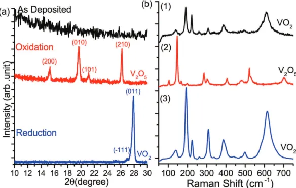
K4B.0:#4)*0.%=874>% The as-grown films using cyclohexane as a liquid carrier (step 1) are XRD-amorphous (Fig. 1a), which contrasts with the crystalline VO2 films obtained with ethanol at this temperature range23. On the
other hand, cyclohexane is thermally more stable than ethanol at 600 °C31. For instance, the pyrolysis of ethanol in
the temperature range 576–624 °C produces essentially methane, hydrogen and oxygen containing compounds as acetaldehyde and carbon monoxide32. In contrast to cyclohexane, ethanol is able to participate into the deposition
chemistry as a potential source of oxygen. It is worth mentioning that the as-grown films represent the VO2
char-acteristic Raman signature (Fig. 1b) but do not feature any obvious sudden change of electrical resistivity upon heating. It is therefore necessary to apply post-deposition treatments to improve the crystallinity of VO2 films and
decrease the density of the grain boundaries.
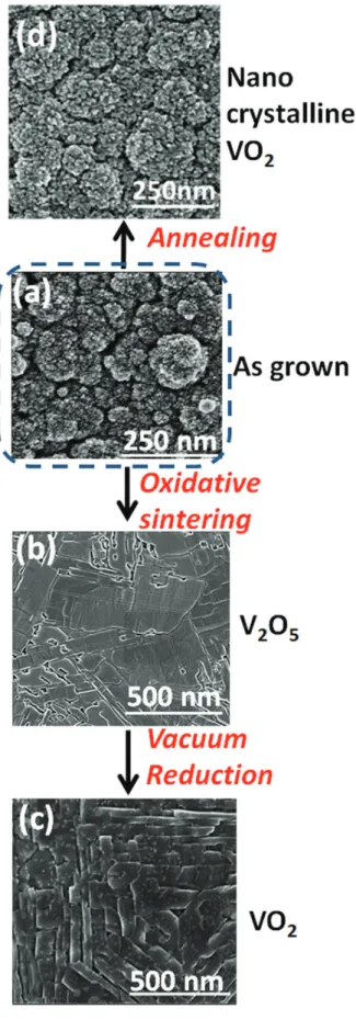
Post deposition thermal treatment. Two approaches were implemented to induce the sintering of VO2 films.
Annealing under vacuum in the absence of oxygen was performed at 600 °C directly in the deposition chamber. As this temperature is far below the melting point (1970 °C) of VO2, no significant sintering took place as shown
in Fig. 2(a–d). The second approach involves the conversion of VO2 to V2O5, that exhibits a lower melting point
(690 °C), prior sintering. This approach proves to be successful as displayed in Fig. 2(a,b). The conversion of VO2
to V2O5 was performed under the O2 partial pressure of 0.01 mbar. The XRD analysis, supplementary information
(S1), shows the occurrence of the VO2 – V2O5 conversion already at 400 °C. Fixing the temperature at 600 °C was
essentially implemented to induce an efficient sintering over a short period (1 h) and to simplify this multi-step process by keeping the substrate temperature constant.
The sintered V2O5 films undergo reduction to VO2 at the same temperature in the absence of oxygen as shown
in Figs 1 and 2. The surface micrographs, Fig. 2a–c, display the evolution of the film microstructure at the various steps of the process from porous nano grains to large and well-shaped domains. Upon reduction under vacuum, V2O5 releases oxygen without significantly affecting the obtained dense morphology (Fig. 2b,c). An extended
treatment under these conditions is expected to yield V2O333.
Figure 1. XRD patterns (a) and Raman spectra (b) of (1) as-grown film, (2) pure phase orthorhombic V2O5 (PDF no-750457) obtained after oxidation and (3) monoclinic VO2 M1 phase (PDF no-03-065-2358)
obtained upon V2O5 annealing under vacuum. The average crystallite size of V2O5 and VO2 is 22 nm and 27 nm
Figure 2. Scanning electron micrographs showing the evolution of film morphology at different stages of film processing from (a) the as-grown amorphous vanadium oxide film, (b) sintered V2O5 film to a (c) sintered VO2
by vacuum reduction. 4 hours annealing of VO2 at 600 °C under vacuum induces a marginal morphological
XRD and Raman scattering, Fig. 1, indicate the nano-crystalline nature of the as-grown VO2 films that are
XRD-amorphous but feature the characteristic VO2 Raman peaks. The oxidative sintering step yields an
orthor-hombic V2O5 that converts into crystalline VO2 (M1) after further annealing under vacuum. Raman spectrum of
the crystalline VO2 features an enhanced scattering intensity.
Film properties. Temperature-programmed X- ray diffraction was carried from room temperature up to 130 °C. Contour plots shown in Fig. 3 point towards an abrupt change of the diffractogram during heating and cooling cycles. Figure 3(a) shows the phase transition of VO2 in the 50–80 °C range whereas Fig. 3(b) presents a closer
look at the changes taking place near the structural phase transition in the 61–70 °C range. The peak at 2θ = 27.9° corresponding to (011), vanishes abruptly at 65–66 °C in the heating cycle. Above this temperature a diffraction peak at 2θ = 27.6° is suddenly detected. The reverse transition occurs at 63–64 °C upon cooling, which reveals a narrow hysteresis width of ~1–2 K. Further detailed X-ray diffraction data can be found in the supplementary section (Figure S2).
The optical reflectivity and thermal imaging were acquired as a function of temperature for 500 nm-thick VO2
films. The wavelength-dependent total hemispherical reflections in the near infrared region (NIR) are displayed in Fig. 4 across the SMT. The thermochromic behavior is clearly shown by an abrupt increase of the reflection
Figure 3. Contour plots of X-ray diffraction during the structural phase transition occurring during heating and cooling stages in the ranges: 50 to 80 °C (a) and 61–70 °C (b).
from e.g. 18% to 55% at λ = 2300 nm by increasing the temperature. Figure 4(b) shows the reflection hysteresis curve at this wavelength. The observed sharp transition and narrow hysteresis, which agree with the XRD results, are relevant assets for energy efficient glazing and static solar control applications10,12,34,35.
Based on the spectroscopic measurements it is clear that the monoclinic and rutile phases of VO2 feature a
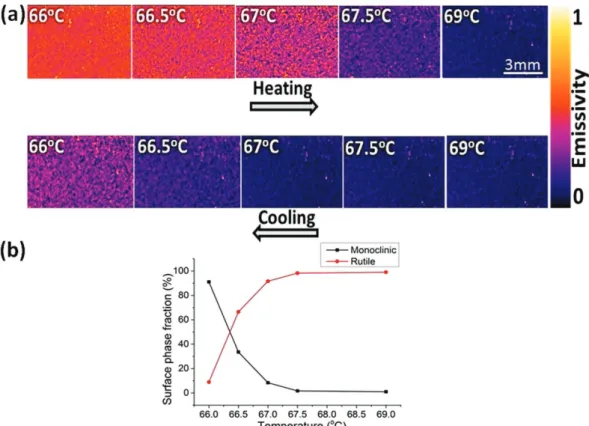
contrasting thermal emissivity. This contrast was represented in the NIR imaging to spatially resolve the phase transition across the SMT. The surface temperature is captured using a neighboring coated silicon with a thick (4–5 µ m) carbon nanotube layer which acts as a perfect black body.
NIR images in Fig. 5a display the evolution of the rutile metallic domains (low emissivity) with increasing temperature across the transition. These domains grow rapidly in size with a small increase in temperature until coalescence. Similar to temperature dependent XRD patterns and NIR reflection behavior, we notice a difference of ∆ T = 1–2 K between the heating and cooling stages, which confirms the small width of the hysteresis curve. The fraction and distribution of the metallic domains at 67–67.5 °C during the heating stage are equivalent to these at 66–66.5 °C in the cooling stage.
In a finite range of temperature (66–69 °C), both semiconducting and metallic phases with contrasting electri-cal and optielectri-cal properties co-exist. One of the early descriptions of VO2 in this range was proposed by H. S. Choi
et al.36 which implemented the corresponding model to simulate the electrical conduction behavior. Later
the same region of phase co-existence was also referred to as “monoclinic and correlated metal” (MCM)37
and “strongly correlated metal”38. The most recent description of this transition state of VO
2 is “disordered
metamaterial”39,40.
Yun Zhang et al.41 report on disordered metal nanoparticles (MNP) in a dielectric matrix, yet still featuring
near perfect metamaterial absorption behavior. Authors successfully show that the order is not necessary to attain controllable metamaterials. Thus VO2 in a finite range of temperature features essentially the same kind of
phys-ical features as the aforementioned MNP in a dielectric matrix, which strengthens the recent identification of vanadium oxide transition state as “disordered metamaterial”.
The dominance of the metallic phase, Fig. 5(a), at 66.5 °C contrasts greatly between the heating and cooling stages. Upon heating, the film is overwhelmingly composed of monoclinic semiconducting phase, whereas, it shows mainly a rutile metallic phase upon cooling. Hence, the self-assembled disordered metamaterial in this temperature range features an appealing modular optical and electrical properties with high thermal sensitivity. The persisting small bright spots in the IR images correspond to surface defects as heterogeneities in surface topography (roughness, micron and submicron thickness, to name some) that influences the IR emissivity42.
Figure 4. Temperature-dependent infrared reflectivity in the NIR region: Reflection spectra in the NIR upon heating (a) and the variation in reflection across the transition temperature (b) displayed for the arbitrary selected wavelength λ = 2300 nm.
The fraction of each phase changes abruptly, Fig. 5b, and the rutile domains grow in size and coalesce to form the majority phase at the transition temperature. The semiconducting and metallic domains co-exist and a small thermal excitation can result in large changes in terms of the self-assembly and the dominance of one phase over the other. The major change occurs essentially in a temperature window of ∆ T = 1 K. On reaching up to 69 °C the film is completely dominated by the R phase, but there is still a tiny fraction of M phase.
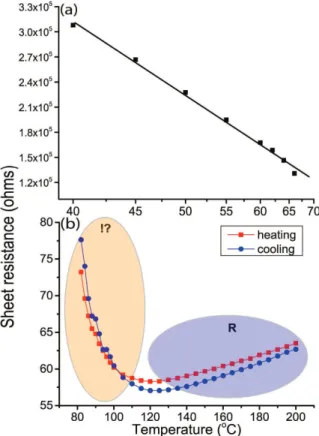
Electrical resistivity was measured as a function of temperature, Fig. 6, for a 500 nm thick film on a Si substrate with its native oxide. The SMT induces an electrical resistivity change exceeding 3 orders of magnitude in the temperature range from 60 to 75 °C. The ratio of sheet resistances R(30 °C)/R(100 °C) gives a value of 0.66 104
(see Fig. 7). The SMT occurs at 67 °C in the heating cycle and the reverse phase transition occurs at 64 °C indicat-ing a hysteresis width of 3 K.
Electrical resistance of the film is a macroscopic property that essentially takes into account the percola-tion between the metallic domains or the kinetics of their formapercola-tion, growth and coalescence. The collective behavior of the film is therefore not representative of the intrinsic microscopic SMT. In the microscopic regime,
Figure 5. (a) Thermal imaging of VO2 film near the phase transition showing the formation of small metallic
clusters as purple spots that grow in size with temperature. (b) The fraction of monoclinic and rutile phases calculated from the change of color in the thermal images during the cooling stage.
isolated metallic domains appear almost instantaneously throughout the film at a much lower temperature (a video is provided as supplementary materials: Figure S3). Besides the formation of new rutile nuclei upon the increase of temperature, the existing domains grow and coalesce43, forming electrically conductive paths by
percolation. It is worth to note that the resistivity of VO2 depends on the coalescence of the metallic domains
rather than their apparition. Therefore, the observed hysteresis for the electrical resistivity should be related to the temperature-dependent kinetics of coalescence or confinement of the metallic domains. The here observed hysteresis width, ∆ T = 3 K, contrasts with the obtained width, ∆ T = 1–2 K, from XRD (Fig. 3), IR reflection (Fig. 4) and thermal imaging (Fig. 5) measurements. The hysteresis in the last cases reflects rather the phase pre-dominance and not the coalescence of the metallic rutile domains.
Further expanding on the electrical properties of the film, we can distinguish the electrical behavior of VO2
into two states, namely a high resistance semiconducting and low resistance metallic region at low and high temperatures respectively. Figure 7a exhibits the expected semiconducting behavior observed below 65 °C where the electrical resistivity decreases with temperature due to the thermal activation of charge carriers. The deduced temperature coefficient of resistance (TCR) and activation energy in the semiconducting region, − 2.6% K−1 and
0.3 eV respectively, agree with values reported for VOx films44–46. A linear increase of the electrical resistance,
Fig. 7b, is observed with temperature above 120 °C indicating the metallic nature with a TCR of + 0.17% K−1 that
concurs with the reported values of common metals and alloys47. Interestingly films feature a metal behavior with
positive TCR only starting at 120 °C, which is far above the SMT temperature.
The electrical resistance continues to decrease above the SMT with temperature, as displayed in Fig. 7b. This hints at the persistence of a semiconducting-like behavior due to competing contribution of the residual semi-conducting phase resulting in a negative coefficient of resistance above the SMT. The occurrence of this behavior equally during the heating and the cooling stages, Fig. 7b, indicates its intrinsic nature. This has been noticed by Zhang et al.48 upon the investigation of the electrical properties of single VO
2 nanobeam within the 70–110 °C
temperature range. Authors could evidence the coexistence of M2 and R phases in this temperature range, and show their comparable electrical resistivity49. Although it seems to be overlooked, the negative TCR above SMT is
visible in results displayed in several reports29,44,49. Jones et al.50 have reported the potential presence of M2 phase
along with R at temperatures significantly higher than the SMT.
Regarding the M2 phase of VO2, Ji et al.51 have reported its presence in epitaxial VO2 and noticed a remarkable
impact of the film’s strain on its dominance and stabilization temperature. Kim et al.37 have interestingly
con-cluded that VO2 undergoes a two-step (M1-M2-R) conversion during the electrically driven transition, which is
in line with static lattice calculations that predict an intermediate phase with a Peierls distortion when approach-ing the phase transition between M1 and the rutile phases52,53. A strong surface-induced stress stabilizes the M2
phase, which is assumed to mediate the transition50,54.
Figure 7. Electrical resistance in semiconducting monoclinic (M) and metallic rutile (R) phases of the VO2 film
in the temperature ranges: (a) 40–65 °C and (b) 80–200 °C. Notice the further decrease in resistance long after the SMT with temperature in the cooling and heating stages.
The presence of M2 would indeed clarify the observed semiconductor behavior after the first order phase transition at 70 °C. Thermal imaging, Fig. 5, does not allow distinguishing M1 from M2 phase because of their presumably similar emissivity values. Raman scattering, however, enables distinguishing these two phases via a significant Ag band shift from 620 cm−1 in M1 to 650 cm−1 in M251. The Raman spectrum of the rutile metallic
phase is devoid of any peaks. Temperature-programmed Raman spectroscopy was implemented to investigate the eventual formation of the M2 phase through the SMT. As displayed in the supplementary information doc-ument, Figure S4, the M2 intermediate phase could be detected, but not systematically even at micrometer dis-tances on the same sample. This seemingly unreliable detection of the M2 phase hints at its localized formation. This observation would agree with the assumption of Ji et al.51 that the formation of M2 phase is likely related
to the presence of tensile stress. It is noteworthy that reports addressing the detection of M2 phase implement high-resolution X-ray diffraction, tip enhanced Raman spectroscopy and localized strain modulation of single crystal nanobeams37,54,55.
Unlike nanobeams, such a stress might be randomly localized in polycrystalline films. Not detecting the M2 phase with XRD (Fig. 3), where the signal is averaged over an area of several square millimeters, indicates that M2 is a minor phase in the entire investigated temperature range.
Therefore, Raman mapping was performed at 67.5 °C for both wavenumbers (M2:650 cm−1 and M1:620 cm−1),
Fig. 8a, to spatially localize the distribution of M1, M2 and R phases. This enables the spatial mapping of polycrys-talline VO2 surface to visualize the random distribution of different phases. Each pixel corresponds to a 1 × 1 µ m2
analysis area. The red dots in Fig. 8a represent M1 phase, whereas the green and yellow dots represent M2 and M1 + M2 domains respectively. The black background illustrates the presence of the R phase of VO2. The spectra
of the aforementioned colored points in the Raman map are displayed in Fig. 8b. Hence, Raman mapping evi-dences clearly the self-assembly of a disordered M1-M2-R metamaterial at the transition temperature. It is worth mentioning that the presence of M2 phase was not evidenced above 70 °C, which is likely due to the excessive dominance of the metallic rutile phase. The entire SEM micrograph, Fig. 2, depicts a certain number of crys-tals and grain boundaries in an area that nearly corresponds to 1 × 1 µ m2, which is the size of a single pixel in
Fig. 8. This means that every single pixel (Fig. 8) contains a large number of grains/crystals and grain boundaries. Therefore, correlating the detection of M2 phase with morphological features such as grain boundary seems unlikely.
Based on the Raman mapping recorded at 67.5 °C, Fig. 8a, and the temperature-programmed Raman meas-urement, Figure S4 in the supplementary information, it could be shown that thermally driven phase transition in polycrystalline VO2 film involves indeed the formation of the M2 phase but in confined locations. It is assumed
that localized strain in these confined areas meets conditions where M2 significantly forms as intermediate phase. It is noteworthy that the film was maintained at this state at 67.5 °C in air for extended periods (100 hrs) with-out any apparent degradation or drift of one state to another. Therefore, the disordered VO2-metamaterial phase
is quite stable and robust, which is an asset to its potential implementation in practical applications.
Vanadium oxide film as a thermally controlled electrical switch. As noticed during the investigation of the spatial phase distribution within VO2, the metamaterial phase is surprisingly stable over extended periods. Therefore, it
Figure 8. (a) Raman surface mapping of the M1, M2, M1 + M2 and R phases as measured at 67.5 °C (each dot correspond to 1 × 1 µ m2 analysis area) and (b) Raman spectra corresponding to the color-coded used in the
is virtually possible to stabilize the system at any point within the hysteresis curve by adjusting the temperature. A practical application of this feature could be a thermally activated electrical switch, which might operate by the supply of short heating and cooling pulses with small amplitudes ∆ T. These pulses bring the metamaterial to cycle between resistive “Off ” and conductive “On” states while keeping the same background temperature around the SMT value.
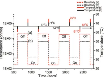
Experimental thermal switching behavior of VO2 is displayed in Fig. 9. At the background temperature 67 °C
the VO2 films feature the disordered metamaterial structure. This temperature is applied using a heating stage
while monitoring the electrical resistance. The highly resistive semiconducting state is considered as an “off ” state. A 3 seconds heating pulse ∆ T drives the coalescence of the metallic rutile domains in the metamaterial, a state that is retained after the back stabilization of the temperature at 67 °C. This behavior originates from the difference between the forward and backward transition temperatures due to hysteresis width as illustrated schematically in Fig. 10. In order to switch the metamaterial back to the “off ” state, a cooling pulse for a short
Figure 9. Thermal switching behavior of the VO2 disordered metamaterial. The “off ” and “on” states are determined by the sudden drop or increase in electrical resistance as a consequence of small changes in the temperature given in the form of thermal activation pulses.
Figure 10. Schematic representation of the thermal switching process based on the hysteresis curve. The impact of adopting two different amplitudes of the thermal activation is illustrated in (i) and (ii). c → a → b: cooling pulse; b → d → c: heating pulse.
duration induces the shrinkage and confinement of the metallic domains. Consequently, the metamaterial fea-tures a resistive semiconducting behavior even when it stabilized back at 67 °C. Hence, short thermal activation pulses are reliably implemented for abrupt manipulation of the electrical properties of VO2 in the metamaterial
state. The amplitude of the thermal pulse activation has a direct impact on the response of VO2 metamaterial as
shown in Figs 9 and 10.
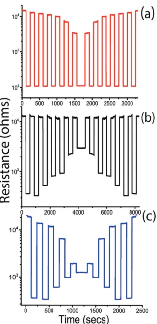
Using high strength of the thermal activation pulse as shown in Fig. 10(i) allows the “on” and “off ” states of the system at points (b) and (d) respectively, thus taking a high benefit of the resistivity change. Whereas a weaker thermal activation pulse as shown in Fig. 10(ii) restricts the amplitude of switching. This enables programing the metamaterial to follow virtually any particular switching pattern. Few such examples are experimentally per-formed and the results are displayed in Fig. 11. Adjusting the strength of the heating and/or cooling pulses allows manipulating the resistance-switching pattern. This degree of flexibility proves the robustness and reliability of this thermally triggered VO2 electrical switching metamaterial.
It is worth noting that attaining high switching amplitude while implementing a small thermal activation requires a sharp transition with a minimal hysteresis width. The narrow hysteresis, ∆ T = 3 K, obtained in this study is equivalent to single crystal or epitaxial films and is ideal for high performance applications25,27. The
self-assembled VO2 disordered metamaterial films operate optimally even after extensive and extended use,
which makes it an attractive candidate for highly demanding applications. The attractiveness of such metamate-rial will substantially enhance, provided a reliable approach is developed for the tuning of the SMT temperature without scarifying its quality in terms of amplitude, sharpness and hysteresis width.
Figure 11. Temperature-programmed resistance switching of the metamaterial via the adjustment of heating (a), cooling (b) or both heating and cooling (c) activation pulses.
Conclusions
Indigenous oxidative sintering approach was implemented in this study to induce an efficient densification of the grown VO2 film. This multistep process was performed in the same CVD reactor without intermediate handling
and air exposure of the samples. The resulting films feature SMT characteristics that match those of epitaxial or bulk VO2 in terms of sharpness and width of the hysteresis. This development paves the way towards the
explo-ration and understanding the behavior of this material. Spatially resolved phase analysis using Raman mapping within the transition regime reveals the self-assembly of VO2 disordered metamaterial that exhibit an outstanding
long-term stability. The formation of locally confined M2 intermediate phase during the transition was attributed to the presence of localized strain. The disordered metamaterial was thermally activated to tune the degree of coalescence/confinement of the metallic domains with high precision. Such a control enables a highly accurate and tunable thermal triggering of the electrical switching.
Methods
Films of vanadium oxide were deposited on silicon substrates using direct liquid injection MOCVD (MC200 from AnnealSys), which is a stagnation point-flow warm-walled reactor. Cyclohexane solution containing 5 × 10⁻³ mol/l
of vanadium (V) oxy-tri-isopropoxide was used as a single-source precursor, which was maintained under nitrogen atmosphere at room temperature before its injection into the evaporation chamber at a frequency of 2 Hz and an adjusted opening time to reach a feeding rate of 1 g/min. The pressure and temperature of the evaporation chamber were maintained at 0.6 mbar and 200 °C during deposition respectively, whereas the walls of the reactor were maintained at 200 °C. During the growth, 500 sccm of nitrogen carrier gas was introduced alongside the precursor injection and the total pressure of the reactor was automatically regulated at 0.6 mbar. The substrate is maintained at 600 °C during the 2 hours of deposition and the subsequent heat treatments.
In a second step, an hour long annealing was performed at 600 °C right after the deposition under oxygen par-tial pressure of 1 × 10⁻² mbar. The sample is then further subjected to annealing at the same temperature under
vacuum (~0.6 mbar) acting as a reducing atmosphere for 4 hours, after which the chamber is allowed to cool down. All depositions were carried out on 4-inch silicon wafers without removing the upper native oxide layer that might act as a barrier. Samples were later cut into smaller pieces for analysis purposes. Uniform, high quality VO2 films were observed throughout the wafers in a homogeneous manner.
L2+5+6*05)I+*)#$>% X-ray diffraction (XRD), Bruker D8, with CuKα as the X-ray source, was used to identify the crystalline phases of vanadium oxide. Data were collected in the θ − 2θ (locked couple) mode from 2θ of 20° to 60° with a step size of 0.02°.
Film thickness was measured using an Alpha step d-500 profilometer from KLA-Tencor and FEI Helios Nanolab 650
™
, Scanning Electron Microscope (SEM). Surface morphology was inspected by SEM at a working distance of 4 mm with an operating voltage of 25 kV.Raman spectroscopy was performed using an InVia Raman spectrometer from Renishaw with a 532 nm laser. In situ temperature-dependent Raman measurements were performed at ambient air with a Linkam TMS heating stage using fixed heating and cooling ramp at 5 °C/min.
The electrical resistivity was measured using four-point probe measurements in Van der Pauw config-uration. Infrared image analysis was conducted using the FLIR X6580SC thermal camera operating in the 1.5–5.1 µ m spectral range with an accurate recording at a frequency of 355 Hz in a full 640 × 512 resolution. Temperature-dependent measurements were performed by placing the sample on a heating stage and cycling the temperature form 40 °C to 80 °C while a thermocouple was placed on the sample to measure the surface temper-ature. The ramp was fixed at 5 °C/min in the transition range.
References
1. Morin, F. J. Oxides Which Show a Metal-to-Insulator Transition at the Neel Temperature. Physical Review Letters 3, 34–36 (1959). 2. Nag, J. & Haglund, R. F. Jr. Synthesis of vanadium dioxide thin films and nanoparticles. J Phys Condens Matter 20, 264016 (2008). 3. Vernardou, D., Pemble, M. & Sheel, D. Vanadium oxides prepared by liquid injection MOCVD using vanadyl acetylacetonate.
Surface and Coatings Technology 188–189, 250254 (2004).
4. Lee, S., Meyer, T., Park, S., Egami, T. & Lee, H. Growth control of the oxidation state in vanadium oxide thin films. Appl Phys Lett
105, 223515 (2014).
5. Liu, D., Zheng, W., Cheng, H. & Liu, H. Thermochromic VO2 Thin Film Prepared by Post Annealing Treatment of V2O5 Thin Film.
Adv Mat Res 79–82, 747–750 (2009).
6. Liu, D., Cheng, H., Zheng, W. & Zhang, C. Infrared thermochromic properties of VO2 thin films prepared through aqueous sol-gel
process. J Wuhan Univ Technology-mater Sci Ed 27, 861–865 (2012).
7. Castro, M., Ferreira, C. & Avillez, R. Vanadium oxide thin films produced by magnetron sputtering from a V2O5 target at room
temperature. Infrared Phys Techn 60, 103–107 (2013).
8. Vernardou, D. et al. A study of the electrochemical performance of vanadium oxide thin films grown by atmospheric pressure chemical vapour deposition. Sol Energ Mat Sol C 95, 2842–2847 (2011).
9. Kam, K. & Cheetham, A. Thermochromic VO2 nanorods and other vanadium oxides nanostructures. Mater Res Bull 41, 1015–1021
(2006).
10. Batista, C., Ribeiro, R. & Teixeira, V. Synthesis and characterization of VO2-based thermochromic thin films for energy-efficient
windows. Nanoscale Res Lett 6, 301 (2011).
11. Saeli, M., Piccirillo, C., Parkin, I., Ridley, I. & Binions, R. Nano-composite thermochromic thin films and their application in energy-efficient glazing. Solar Energy Materials and Solar Cells 94, 141–151 (2010).
12. Kamalisarvestani, Saidur, Mekhilef & Javadi, F. S. Performance, materials and coating technologies of thermochromic thin films on smart windows. Renewable and Sustainable Energy Reviews 26, 353–364 (2013).
13. Zhang, Z. et al. Thermochromic VO2 thin films: solution-based processing, improved optical properties, and lowered phase
transformation temperature. Langmuir 26, 10738–44 (2010).
14. Perucchi, A., Baldassarre, L., Postorino, P. & Lupi, S. Optical properties across the insulator to metal transitions in vanadium oxide compounds. Journal of Physics: Condensed Matter 21, 323202 (2009).
16. Bahlawane, N. & Lenoble, D. Vanadium Oxide Compounds: Structure, Properties, and Growth from the Gas Phase. Chemical Vapor Deposition 20, 299–311 (2014).
17. Guzman, G., Morineau, R. & Livage, J. Synthesis of vanadium dioxide thin films from vanadium alkoxides. Mater Res Bull 29, 509–515 (1994).
18. Gao, W., Wang, C. M., Wang, H. Q., Henrich, V. E. & Altman, E. I. Growth and surface structure of vanadium oxide on anatase (001). Surface science 2–3, 201–213 (2004).
19. Peter, A. P. et al. Metal Insulator Transition in ALD VO2 Ultrathin Films and Nanoparticles: Morphological Control. Adv Funct
Mater 25, 679–686 (2015).
20. Cazzanelli, E., Mariotto, G., Passerini, S., Smyrl, W. H. & Gorenstein, A. Raman and XPS characterization of vanadium oxide thin films deposited by reactive RF sputtering. Solar energy materials and solar cells 56, no. 3 249–258 (1999).
21. Mantoux, A., Groult, H., Balnois, E., Doppelt, P. & Gueroudji, L. Vanadium Oxide Films Synthesized by CVD and Used as Positive Electrodes in Secondary Lithium Batteries. J Electrochem Soc 151, A368 (2004).
22. Crociani, L., Carta, G., Natali, M., Rigato, V. & Rossetto, G. MOCVD of Vanadium Oxide Films with a Novel Vanadium(III) Precursor. Chem Vapor Depos 17, 6–8 (2011).
23. Kumar, S., Lenoble, D., Maury, F. & Bahlawane, N. Synthesis of vanadium oxide films with controlled morphologies: Impact on the metal–insulator transition behaviour. Phys Status Solidi 212, 1582–1587 (2015).
24. Martens, K., Aetukuri, N., Jeong, J., Samant, M. & Parkin, S. Improved metal-insulator-transition characteristics of ultrathin VO2
epitaxial films by optimized surface preparation of rutile TiO2 substrates. Appl Phys Lett 104, 081918 (2014).
25. Ji, Y. D., Pan, T. S., Bi, Z., Liang, W. Z. & Zhang, Y. Epitaxial growth and metal-insulator transition of vanadium oxide thin films with controllable phases. Appl. Phys. Lett. 101, 071902 (2012).
26. Muraoka, Y. & Hiroi, Z. Metal-insulator transition of VO2 thin films grown on TiO2 (001) and (110) substrates. Applied physics letters 80.4, 583–585 (2002).
27. Mansingh, A., Ramadhar, Singh & Krupanidhi, S. B. Electrical switching in single crystal VO2. Solid-State Electronics 23.6, 649–654
(1980).
28. Klimov, V. A. et al. Hysteresis loop construction for the metal-semiconductor phase transition in vanadium dioxide films. Technical Physics 47, no. 9 1134–1139 (2002).
29. Rampelberg, G. et al. In situ X-ray diffraction study of the controlled oxidation and reduction in the V–O system for the synthesis of VO2 and V2O3 thin films. Journal of Materials Chemistry C 3.43, 11357–11365 (2015).
30. Dreizin, E. L., Allen, D. J. & Glumac, N. G. Depression of melting point for protective aluminum oxide films. Chemical Physics Letters 618, 63–65 (2015).
31. Billaud, Francis, Marc Duret, Khalid Elyahyaoui & Francois, Baronnet. Survey of recent cyclohexane pyrolysis literature and stoichiometric analysis of cyclohexane decomposition. Industrial & Engineering Chemistry Research 30, no. 7: 1469–1478 (1991). 32. Barnard, J. A. & Hughes, H. The pyrolysis of ethanol. Transactions of the Faraday Society (1960).
33. Su, Dang Sheng & Robert, Schlögl. Thermal decomposition of divanadium pentoxide V2O5: Towards a nanocrystalline V2O3 phase.
Catalysis letters 83.3-4, 115–119 (2002).
34. Seeboth, Arno, Schneider, Johannes & Andre, Patzak. Materials for intelligent sun protecting glazing. Solar energy materials and solar cells 60.3, 263–277 (2000).
35. Parkin, Ivan P. & Troy D. Manning. Intelligent thermochromic windows. J. Chem. Educ 83.3, 393 (2006).
36. Choi, H. S., Ahn, J. S., Jung, J. H., Noh, T. W. & Kim, D. H. Mid-infrared properties of a VO2 film near the metal-insulator transition.
Physical Review B 54, no. 7 4621 (1996).
37. Kim, B.-J. et al. Micrometer x-ray diffraction study of VO2 films: Separation between metal-insulator transition and structural phase
transition. Phys Rev B 77 (2008).
38. Qazilbash, M. et al. Mott Transition in VO2 Revealed by Infrared Spectroscopy and Nano-Imaging. Science 318, 1750–1753 (2007).
39. Kats, M. A. et al. Vanadium dioxide as a natural disordered metamaterial: perfect thermal emission and large broadband negative differential thermal emittance” Physical Review X 3.4, 041004 (2013).
40. Kats, M. A. et al. Ultra-thin perfect absorber employing a tunable phase change material. Applied Physics Letters 101, no. 22 221101 (2012).
41. Zhang, Y. et al. Vapor-deposited amorphous metamaterials as visible near-perfect absorbers with random non-prefabricated metal nanoparticles. Scientific reports 4 (2014).
42. Maury, F. & Duminica, F.-D. Diagnostic in TCOs CVD processes by IR pyrometry. Thin Solid Films 515.24, 8619–8623 (2007). 43. Madan, H., Jerry, M., Pogrebnyakov, A., Mayer, T. & Datta, S. Quantitative Mapping of Phase Coexistence in Mott-Peierls Insulator
during Electronic and Thermally Driven Phase Transition. Acs Nano 9, 2009–2017 (2015).
44. Venkatasubramanian, C., Horn, M. W. & Ashok, S. Ion implantation studies on VOx films prepared by pulsed dc reactive sputtering.
Nuclear Instruments and Methods in Physics Research Section B: Beam Interactions with Materials and Atoms 267, 1476–1479 (2009). 45. Han, Y.-H. et al. Fabrication of vanadium oxide thin film with high-temperature coefficient of resistance using V2O5/V/V2O5
multi-layers for uncooled microbolometers. Thin Solid Films 425.1, 260–264 (2003).
46. Ko, Changhyun & Ramanathan, Shriram Observation of electric field-assisted phase transition in thin film vanadium oxide in a metal-oxide-semiconductor device geometry. Applied Physics Letters 93.25, 2101 (2008).
47. Weast, R. C. Handbook of chemistry and physics. The American Journal of the Medical Sciences 257, 423 (1969).
48. Zhang, S., Chou, J. & Lauhon, L. Direct correlation of structural domain formation with the metal insulator transition in a VO2
nanobeam. Nano Lett 9, 4527–32 (2009).
49. Zhang, H.-T. et al. Wafer-scale growth of VO2 thin films using a combinatorial approach. Nature Communications 6, 8475 (2015).
50. Jones, A., Berweger, S., Wei, J., Cobden, D. & Raschke, M. Nano-optical investigations of the metal-insulator phase behavior of individual VO2 microcrystals. Nano letters 10, 1574–81 (2010).
51. Ji, Y. et al. Role of microstructures on the M1-M2 phase transition in epitaxial VO2 thin films. Scientific reports 4854 (2014).
52. Pouget, J. P. et al. Dimerization of a linear Heisenberg chain in the insulating phases of V1− xCrxO2. Physical Review B 10.5, 1801
(1974).
53. Whittaker, L., Patridge, C. & Banerjee, S. Microscopic and Nanoscale Perspective of the Metal− Insulator Phase Transitions of VO2
Some New Twists to an Old Tale. J Phys Chem Lett 2, 745–758 (2011).
54. Sohn, J. I. et al. Surface-stress-induced Mott transition and nature of associated spatial phase transition in single crystalline VO2
nanowires. Nano Lett. 9, 3392–7 (2009).
55. Kim, M.-W. et al. Substrate-mediated strain effect on the role of thermal heating and electric field on metal-insulator transition in vanadium dioxide nanobeams. Scientific reports 5 (2015).
K6,$#A80.-070$*4
The authors would like to acknowledge Luxembourg Institute of Science and Technology (LIST) for providing the financial support for this work.
Author Contributions
S.K. performed the synthesis and characterization of the coatings under the supervision of N.B., S.K. and N.B. wrote the manuscript, and all authors iteratively discussed the results and provided comments.
Additional Information
Supplementary information accompanies this paper at http://www.nature.com/srep
Competing financial interests: The authors declare no competing financial interests.
How to cite this article: Kumar, S. et al. Electrical Switching in Semiconductor-Metal Self-Assembled VO2