HAL Id: pastel-00843104
https://pastel.archives-ouvertes.fr/pastel-00843104
Submitted on 10 Jul 2013
HAL is a multi-disciplinary open access
archive for the deposit and dissemination of sci-entific research documents, whether they are pub-lished or not. The documents may come from teaching and research institutions in France or abroad, or from public or private research centers.
L’archive ouverte pluridisciplinaire HAL, est destinée au dépôt et à la diffusion de documents scientifiques de niveau recherche, publiés ou non, émanant des établissements d’enseignement et de recherche français ou étrangers, des laboratoires publics ou privés.
Nanocomposite coatings based on quaternary
metalnitrogen
Michael Walock
To cite this version:
Michael Walock. Nanocomposite coatings based on quaternary metalnitrogen. Autre. Ecole nationale supérieure d’arts et métiers - ENSAM; University of Alabama at Birmingham, 2012. Français. �NNT : 2012ENAM0037�. �pastel-00843104�
Doctorat ParisTech
T H È S E
en cotutelle internationale
pour obtenir le grade de docteur délivré par
l’École Nationale Supérieure d'Arts et Métiers
Spécialité “Mécanique et Matériaux”
et
pour obtenir le grade de PhD délivre par
University of Alabama at Birmingham
Spécialité “Physics”
!École doctorale n° 432 : Sciences des Métiers de l’Ingénieur
2012-ENAM-0037
T
H
È
S
E
JuryM. Nicolas MARTIN, Professeur, FEMTO-ST, ENSMM Besancon Président M. Luc IMHOFF, Professeur, ICB, U-Bourgogne Rapporteur M. Mark L. WEAVER, Professor, Dept. of Metallurgical & Materials Engineering, U-Alabama Rapporteur M. S. Aaron CATLEDGE, Assistant Professor, Dept. of Physics, UAB Examinateur Mme. Corinne NOUVEAU, Maitre de Conférences-HDR, LaBoMaP, A & M ParisTech-Cluny Examinateur M. Andrei V. STANISHEVSKY, Associate Professor, Dept. of Physics, UAB Examinateur
M. Yogesh K. VOHRA, Professor, Dept. of Physics, UAB Examinateur présentée et soutenue publiquement par
Michael J. WALOCK
le 1 novembre 2012
Nanocomposite coatings based on quaternary
metal-nitrogen and nanocarbon systems
Copyright by Michael J. Walock
Indeed, what is there that does not appear marvelous when it comes to our knowledge for the first time? How many things, too, are looked upon as quite impossible until they have been actually effected?
NANOCOMPOSITE COATINGS BASED ON QUATERNARY METAL-NITROGEN AND NANOCARBON SYSTEMS
MICHAEL J. WALOCK PHYSICS
ABSTRACT
For this project, CrN-WC coatings are investigated as a hybrid hard and tough material. The use of a hard-carbide with a corrosion-resistant nitride may produce tailored coatings with the desired combination of properties for use as a stand-alone protective coating, or as a basis for nanocrystalline diamond deposition. The work is divided into three stages. The initial study determined the viability of the CrN-WC system, and its use as an interlayer for nanocrystalline diamond. This successful study was followed by a variation of deposition conditions at low
deposition temperature. By varying the deposition parameters, the microstructure, chemical, mechanical, and tribological behavior may be optimized. While the system has relatively good adhesion to silicon substrates, its adhesion to steel was lacking. Additionally, the system showed lower than expected mechanical
properties. The final step increased the deposition temperature. The aim here was to increase adhesion and improve the mechanical properties. Prior results with other systems show consistent improvement of mechanical properties at elevated deposition temperatures. The high deposition temperature coatings showed marked improvement in various characteristics over their low deposition temperature
cousins.
ACKNOWLEDGEMENTS
For me, this has been a very long journey. First, I would like to thank my advisors, Andrei Stanishevsky and Corinne Nouveau. Not only have they been extremely generous with their invaluable time, comments, and suggestions, they are also directly responsible for initiating this unique opportunity of a co-tutelle
between the University of Alabama at Birmingham and Arts et M´etiers ParisTech. Next, I would like to thank Nicolas Martin for serving as president, Luc Imhoff and Mark Weaver for serving as reporters, and my examiners: Yogesh Vohra and S. Aaron Catledge. Their comments and suggestions have been a key
component of this work.
I would also like to thank the combined administrations of the University of Alabama at Birmingham and Arts et M´etiers ParisTech for their support of this tremendous opportunity. Specific thanks go out to G´erard Coffignal and Penny Whiteside.
While it would be impossible to thank everyone who has contributed and/or helped along the way, I would like to specifically thank Romaric Masset, Aur´elien Besnard, Denis Lagadrill´ere, Issam Rahil, Nasser Beliardouh, Ahcene Siad, Amel Zairi, Philippe Steyer, Fr´ed´eric Herbst, Ludovic Largeau, Philippe Perez, Franck S´en´equier, Rich Martens, Johnny Goodwin, Rob Holler, Dan Stockinger, Damian Batory, Marcin Go�l¸abczak, Jeff Montgomery, Jerry Sewell, and Yujiao Zou. All have provided immeasurable assistance with their time, suggestions, and experimental skills. And I cannot forget the assistance of Claude Roy, Florence Dumard, Carole Wahnoun, Christine Loudot, Nathalie Laroche, Hicham Ghossein, Catherine Dani´elou, Amanda Holt, and Mark Case.
Last, but far from least, I would like to thank my friends and family.
Especially, I would like to thank my immediate family: Steve, (in loving memory of) Karen, Christopher, Audrey, Eric, and Jennifer. I would have never made it this far without their undying love and support.
The project described in this dissertation was primarily supported by the U.S. National Science Foundation’s Materials World Network (DMR-08606521) and the French Regional Council of Burgundy. Additional funding for travel was
supported by the U.S. National Science Foundation (OISE-0854945, OISE-1027692). Instrumentation was supported via the U.S. National Science Foundation
(DMR-0922910, DMR-1040474) and by the U.S. National Institute of Arthritis and Musculoskeletal and Skin Diseases (R01AR056665). And finally, part of this work was performed at the Central Analytical Facility, which is supported by The University of Alabama.
TABLE OF CONTENTS DEDICATION . . . iii ABSTRACT . . . iv ACKNOWLEDGEMENTS . . . v LIST OF TABLES . . . x LIST OF FIGURES . . . xi
LIST OF ABBREVIATIONS . . . xviii
CHAPTER I. INTRODUCTION . . . 1
1.1 Overview . . . 1
1.2 Introduction to Protective Coatings . . . 2
1.3 Types of Protective Coatings . . . 2
1.3.1 Binary Compounds . . . 6
1.3.2 Ternary Coatings . . . 7
1.3.3 Structural modifications . . . 8
1.4 Materials selection for protective coatings . . . 15
1.5 CrN-WC material system . . . 16
II. METHODOLOGY . . . 18
2.1 Experimental Design . . . 18
2.2 Deposition . . . 19
2.2.1 Sputter Deposition . . . 19
2.2.2 Chemical Vapor Deposition . . . 24
2.2.3 Effects of Deposition Parameters on Film Structure 28 2.3 Characterization . . . 32
2.3.1 Atomic Force Microscopy . . . 32
2.3.2 Scanning Electron Microscopy . . . 33
2.3.3 Energy Dispersive X-ray Spectroscopy . . . 37
2.3.4 X-ray Diffraction . . . 38
2.3.5 Raman Spectroscopy . . . 43
2.3.7 Optical Profilometry . . . 51
2.3.8 Nanoindentation . . . 55
2.3.9 Scratch testing . . . 60
2.3.10 Corrosion . . . 62
III. RESULTS AND DISCUSSION . . . 65
3.1 Viability of the CrN-WC System . . . 65
3.1.1 Feasibility and Properties of CrN-WC Coatings . . . 65
3.1.2 Nanocrystalline Diamond Deposition on CrN-WC . 71 3.1.3 Summary of the Viability Study . . . 75
3.2 Variation of Deposition Conditions of CrN-WC Films at Low Deposition Temperature . . . 76
3.2.1 Fixed Sputtering Power . . . 77
3.2.2 Fixed Gas Mixture . . . 88
3.2.3 Summary for the low-temperature deposition of CrN-WC coatings . . . 103
3.3 Variation of Deposition Conditions of CrN-WC Films at High Deposition Temperature . . . 106
3.3.1 Thin films at Variable Temperature . . . 109
3.3.2 Nanocrystalline Diamond Deposition on CrN-WC Thin Films . . . 121
3.3.3 Coatings at High Temperature . . . 125
3.3.4 Summary for the high-temperature deposition of CrN-WC coatings . . . 141
IV. CONCLUSIONS AND PERSPECTIVES . . . 145
4.1 Summary of the Viability Study . . . 145
4.2 Summary for the low-temperature deposition of CrN-WC coat-ings . . . 146
4.2.1 Varying the reactive gas mixture . . . 146
4.2.2 Varying the applied sputtering power . . . 148
4.3 Summary for the high-temperature deposition of CrN-WC coat-ings . . . 150
4.3.1 High-temperature CrN-WC thin films . . . 150
4.3.2 High-temperature CrN-WC coatings . . . 151
4.4 Perspectives . . . 154
4.4.1 Further tests on the current material: CrN-WC . . . 154
4.4.2 Improving the current material: CrN-WC . . . 156
4.4.3 Towards other materials of interest . . . 157
APPENDICES . . . 174
A. R´esum´e en fran¸cais . . . 174
A.1 Introduction . . . 175
A.2 M´ethodologie . . . 177
A.3 R´esultats et Discussion . . . 178
A.3.1 Etude de faisabilit´e . . . 178
A.3.2 D´epˆot de CrN-WC obtenus sans chauffage . . . 179
A.3.3 D´epˆots de CrN-WC obtenus en chauffant . . . 183
LIST OF TABLES Table
1.1 Properties of binary metallic hard materials [16]. . . 4 1.2 Properties of binary covalent and ionic hard materials [16]. . . 5 1.3 Properties of structurally modified protective coatings [62]. . . 14 2.1 Deposition conditions for growth of nanocrystalline-Diamond (nc-D)
coatings. . . 27 2.2 The extinction conditions and relationship between the lattice
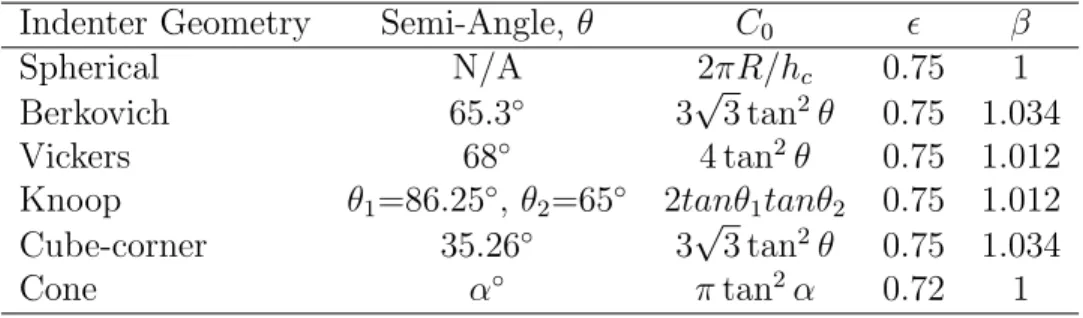
spac-ing and the diffraction plane for the different types of crystalline lattices. . . 42 2.3 Geometrically dependent values of the constant C0. . . 58
2.4 Experimental techniques and the studied sample properties. . . 64 3.1 Deposition conditions for the viability study of CrN-WC coatings.
For improved adhesion, a 170 nm Cr coating is deposited onto the bare substrates. . . 65 3.2 Deposition conditions for the low deposition temperature study of
CrN-WC coatings, with variable gas mixture. . . 77 3.3 Energy Dispersive X-ray Spectroscopy (EDS) results of the CrN-WC
coatings created by varying the gas mixture, deposited on Si. . . 78 3.4 Deposition conditions for the low deposition temperature study of
CrN-WC coatings, with fixed Ar/N2 gas mixture and deposited on Si. 89
3.5 EDS results of the CrN-WC coatings created by varying the Cr:W ratios, deposited on Si. . . 91 3.6 Deposition conditions for the high deposition temperature study of
CrN-WC coatings. . . 108 3.7 EDS results of the CrN-WC thin films created by varying the growth
temperature, deposited on Si. . . 110 3.8 Thickness of CrN-WC thin films created by varying the growth
tem-perature, deposited on Si. . . 117 3.9 EDS results of the CrN-WC coatings created by varying the growth
temperature, deposited on Si. . . 127 3.10 Scratch test results of the CrN-WC coatings, grown at high
temper-ature on Si substrates. . . 140 4.1 Possible deposition conditions for investigating the CrN-WC
coat-ing system. Only those coatcoat-ings marked (X) have been created and characterized. . . 157
LIST OF FIGURES Figure
1.1 Schematic diagram of a TiN/VN superlattice structure, based on the results of Helmersson, et al. [60]. The complete 2.5 µm coating consists of 480 layers of 2.6 nm thick TiN and 2.6 nm thick VN. . . 8 1.2 High-resolution transmission electron micrograph of TiN/SiN
nanocom-posite coating. The (111) and (200) lattice planes of TiN nanocrystals are clearly visible, due to their orientation with respect to the elec-tron beam. These nearly spherical crystallites are surrounded by an amorphous Si3N4 matrix [92]. . . 11
2.1 Schematic of the sputtering process. . . 20 2.2 A used 4-in Cr target which shows the characteristic racetrack of
magnetron sputtering, and the beginning of target ”burn-through,” i.e. the cracking observed in the lower part of the target resulting from extensive use. . . 21 2.3 The modified Nordiko 3500 sputtering system used for depositing the
CrN-WC coatings, located at Laboratoire Bourguignon des Mat´eriaux et Proc´ed´es (LaBoMaP), Cluny, France. The inset shows the interior of the chamber, and the arrangement of the substrate holder with respect to the two 4-in, confocally-arranged magnetron sputtering guns. . . 22 2.4 (a) The 8-in diameter substrate holder and (b) the 4-in× 4-in custom
substrate heater for the Nordiko vacuum system. These images are not to scale; when mounted, the substrate heater moves the samples about 1 cm closer to the sputtering guns. . . 23 2.5 Vacuum diagram of the modified Nordiko 3500 sputtering system. . 24 2.6 The 6 kW, 2.4 GHz Wavemat MPDR microwave-plasma chemical
va-por deposition system. This system is used to deposit nanocrystalline diamond films at University of Alabama at Birmingham (UAB), Birmingham, AL USA. The inset shows a typical plasma during de-position. . . 27 2.7 An extended version of the film structural zone diagram for
ener-getic depositions which includes plasma and ion effects on thin film growth [169]. The main axes are the generalized temperature T∗, the
normalized energy flux E∗, and the net thickness t∗. Zone boundaries
are gradual, and for illustration only. . . 30 2.8 Schematic drawing of (a) the typical Scanning Electron Microscope
2.9 Pictures of (a) a JEOL JSM-6400F [171] (Laboratoire Interdisci-plinaire Carnot de Bourgogne (ICB), Dijon, France), (b) a FEI Quanta 650 [172] (UAB, Birmingham, AL USA), and (c) a JEOL JSM-5900LV (LaBoMaP, Cluny, France). The JEOL JSM-JSM-5900LV is equipped with an Oxford INCA x-act EDS/Wavelength Dispersive X-ray Spec-troscopy (WDS) system. . . 36 2.10 Energy Dispersive X-ray Spectroscopy (EDS) spectrum from a
ce-mented carbide (WC-6 weight (wt.) %-Co) coating on Si. . . 38 2.11 Schematic drawing for meeting the Bragg condition. The wavefront
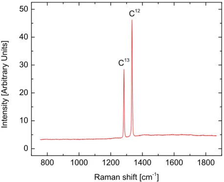
scattered from particles on the interior plane must travel an addi-tional path-length of 2d sin θ to remain in-phase with the scattered wavefronts from the external plane. . . 40 2.12 Raman spectrum from a single-crystal diamond with a coating of C13
diamond. . . 44 2.13 This Dilor XY Raman spectrometer, located at UAB, Birmingham,
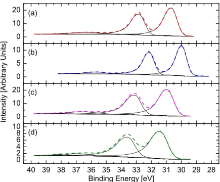
AL USA, uses a 532 nm, 300 mW laser as its source, which can be focused to a 100 µm, spot size. Different neutral density filters can be used to reduce the intensity of the light irradiating the sample. . 45 2.14 Schematic representation of the photoelectric effect. . . 46 2.15 (a) Survey scan of a CrN sample, deposited by Radio-Frequency (RF)
magnetron sputtering. (b) High-resolution scan of the N1s peak. For this high-resolution scan, solid lines are the deconvoluted peaks (identifying the relevant chemical states present), and the dashed lines are the original data. Both scans were taken after 15 minutes of sputter etching with Ar at 1 kV accelerating voltage. . . 47 2.16 This is the PHI5000 Versaprobe, with (a) load-lock, (b) Ar ion gun,
(c) hemispherical analyzer, (d) focused x-ray source, (e) dual x-ray source, and (f) variable-temperature sample stage. This system is located at UAB, Birmingham, AL USA . . . 50 2.17 (a) A schematic diagram of an optical interferometer. (b) An image
of interference fringes of a ruler, using a ZeMetrics profilometer [181]. 53 2.18 The Veeco-Wyko NT1100 optical profilometer, located at LaBoMaP,
Cluny, France. This unit is mounted on an air-table to reduce the effects of vibration. . . 54 2.19 A typical load-displacement curve from the fused silica calibration
standard. ”Loading” indicates the region of increasing load. ”Un-loading” is the region of decreasing load. The hysteresis between the two regions is ”WP,” the plastic work of indentation. . . 57
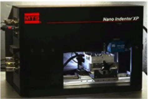
2.20 The NanoIndenter XP by MTS, located at UAB, Birmingham, AL USA. . . 60
2.21 A 5 mm scratch produced by progressive loading of 30 N on a Cr-WC coating on XC100 (AISI 1095) steel. Following the same path (from left to right) as the track, the first inset is an optical micrograph of the track at the first critical load, LC1. Next to this image is a profile
of the scratch scar. The shaded area is the coating thickness. This is followed by optical micrographs of the second critical load, LC2, and
the third critical load, LC3. . . 62
3.1 X-ray diffractograms of samples (a) WC, (b) Cr-WC, (c) WCN, and (d) CrN-WC deposited onto Si. Note, there is a 170 nm Cr buffer layer underneath the top coating. . . 66 3.2 C1s spectra from the (a) WC, (b) Cr-WC, (c) WCN, and (d)
CrN-WC samples. The solid lines are the deconvoluted peaks used for fitting the original data (dashed lines). . . 67 3.3 W4f spectra from the (a) WC, (b) Cr-WC, (c) WCN, and (d)
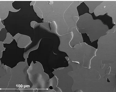
CrN-WC samples. The solid lines are the deconvoluted peaks used for fitting the original data (dashed lines). . . 67 3.4 High-Resolution Scanning Electron Microscope (HR-SEM) image of
the partially delaminated surface of a WC sample on Si. . . 68 3.5 Cr2p spectra from the (a) Cr-WC and (b) CrN-WC samples. The
solid lines are the deconvoluted peaks used for fitting the original data (dashed lines). . . 69 3.6 N1s spectra from the (a) WCN and (b) CrN-WC samples. The solid
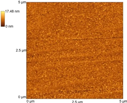
lines are the deconvoluted peaks used for fitting the original data (dashed lines). . . 69 3.7 Atomic Force Microscopy (AFM) micrograph of the CrN-WC sample
deposited on Si. . . 72 3.8 X-ray diffractogram of nc-D film on (a) WCN and (b) CrN-WC
coat-ings, deposited on Si. . . 73 3.9 Raman spectra from the nc-D coating with (a) WCN and (b)
CrN-WC samples acting as a base layer. The substrates are commercially-pure Ti discs. . . 74 3.10 HR-SEM image of the CrN-WC sample after nc-D deposition. The
inset shows an 5×5 µm2 AFM micrograph. . . . 75
3.11 W4f spectra from the CrN-WC samples (deposited on Si) with vary-ing gas mixture: (a) Ar/N2 = 40/60, (b) Ar/N2 = 60/40 , and (c)
Ar/N2 = 80/20. The solid lines are the deconvoluted peaks used for
fitting the original data (dashed lines). . . 80 3.12 C1s spectra from the CrN-WC samples (deposited on Si) with varying
gas mixture: (a) Ar/N2 = 40/60, (b) Ar/N2 = 60/40 , and (c) Ar/N2
= 80/20. The solid lines are the deconvoluted peaks used for fitting the original data (dashed lines). . . 80 3.13 Cr2p spectra from the CrN-WC samples (deposited on Si) with
vary-ing gas mixture: (a) Ar/N2 = 40/60, (b) Ar/N2 = 60/40 , and (c)
Ar/N2 = 80/20. The solid lines are the deconvoluted peaks used for
3.14 N1s spectra from the CrN-WC samples (deposited on Si) with varying gas mixture: (a) Ar/N2 = 40/60, (b) Ar/N2 = 60/40 , and (c) Ar/N2
= 80/20. The solid lines are the deconvoluted peaks used for fitting the original data (dashed lines). . . 81 3.15 O1s spectra from the CrN-WC samples (deposited on Si) with varying
gas mixture: (a) Ar/N2 = 40/60, (b) Ar/N2 = 60/40 , and (c) Ar/N2
= 80/20. The solid lines are the deconvoluted peaks used for fitting the original data (dashed lines). . . 82 3.16 X-ray diffractogram for the CrN-WC (deposited on Si) produced by
varying the gas mixture: (a) Ar/N2 = 40/60, (b) Ar/N2 = 60/40,
and (c) Ar/N2 = 80/20. . . 83
3.17 High-resolution scanning electron micrographs for the CrN-WC (de-posited on Si) produced by varying the gas mixture: (a) Ar/N2 =
40/60, (b) Ar/N2 = 60/40, and (c) Ar/N2 = 80/20. . . 84
3.18 Open circuit porosity results for CrN-WC coatings produced by vary-ing the gas composition. These measurements were taken for samples grown on XC100 steel. . . 86 3.19 Surface roughness parameters of CrN-WC coatings deposited on Si,
and grown with varying gas mixtures. . . 86 3.20 The (a) Young’s Modulus (E) and (b) Hardness (H) results from
the three CrN-WC coatings developed at various Ar/N2 ratios. To
avoid substrate effects, the values are appraised at 5 % of the coating thickness. . . 87 3.21 X-ray Diffraction (XRD) diffractogram of the CrN-WC samples
(de-posited on Si), with varying Cr:W ratios: (a) Cr:W = 4:1, (b) Cr:W = 3:1, (c) Cr:W = 2:1 (d) Cr:W = 1.5:1, and (e) Cr:W = 1:1. The remaining panel shows the Powder Diffraction File (PDF) peaks of cubic- (c-)WN, c-WC1−x, and c-CrN. . . 90
3.22 W4f spectra from the CrN-WC samples (deposited on Si) with vary-ing metal content: (a) Cr:W = 4:1, (b) Cr:W = 3:1 , (c) Cr:W = 2:1, (d) Cr:W = 1.5:1, and (e) Cr:W = 1:1 samples. The solid lines are the deconvoluted peaks used for fitting the original data (dashed lines). 92 3.23 C1s spectra from the CrN-WC samples (deposited on Si) with varying
metal content: (a) Cr:W = 4:1, (b) Cr:W = 3:1 , (c) Cr:W = 2:1, (d) Cr:W = 1.5:1, and (e) Cr:W = 1:1 samples. The solid lines are the deconvoluted peaks used for fitting the original data (dashed lines). 92 3.24 Cr2p spectra from the CrN-WC samples (deposited on Si) with
vary-ing metal content: (a) Cr:W = 4:1, (b) Cr:W = 3:1 , (c) Cr:W = 2:1, (d) Cr:W = 1.5:1, and (e) Cr:W = 1:1 samples. The solid lines are the deconvoluted peaks used for fitting the original data (dashed lines). 93 3.25 N1s spectra from the CrN-WC samples (deposited on Si) with varying
metal content: (a) Cr:W = 4:1, (b) Cr:W = 3:1 , (c) Cr:W = 2:1, (d) Cr:W = 1.5:1, and (e) Cr:W = 1:1 samples. The solid lines are the deconvoluted peaks used for fitting the original data (dashed lines). 93
3.26 O1s spectra from the CrN-WC samples (deposited on Si) with varying metal content: (a) Cr:W = 4:1, (b) Cr:W = 3:1 , (c) Cr:W = 2:1, (d) Cr:W = 1.5:1, and (e) Cr:W = 1:1 samples. The solid lines are the deconvoluted peaks used for fitting the original data (dashed lines). 94 3.27 Open circuit porosity of the CrN-WC coatings deposited at low
de-position temperature, and at fixed gas mixture; deposited on XC100 steel. . . 94 3.28 Optical micrographs of the post-electrochemical test (for open circuit
porosity) surfaces (deposited on XC100 steel): (a) Cr:W = 4:1, (b) Cr:W = 3:1, (c) Cr:W = 2:1, (d) Cr:W = 1.5:1, and (e) Cr:W = 1:1. 95 3.29 Surface topography and cross-sectional HR-SEM micrographs of the
(a) Cr:W = 4:1, (b) Cr:W = 3:1, (c) Cr:W = 2:1, (d) Cr:W = 1.5:1, and (e) Cr:W = 1:1 samples developed at a fixed gas mixture and deposited on Si. . . 96 3.30 Using a 5 × 5 µm2 scan, AFM determined the surface roughness of
the CrN-WC coatings developed at a fixed gas mixture and deposited on Si. . . 97 3.31 Nanoindentation results for the (a) Young’s modulus and (b)
Hard-ness for the CrN-WC coatings developed with a constant gas mixture and deposited on Si. . . 98 3.32 Compressive stress of CrN-WC samples deposited on Si, at low fixed
Ar/N2 ratio and low deposition temperature. . . 102
3.33 C1s spectra for the CrN-WC coatings deposited at various temper-ature. The spectra on the left are from the Cr:W = 0.5:1 samples, with (a) 400 ◦C, (b) 250 ◦C, (c) 180 ◦C, and (d) No External Heat-ing (NEH). Similarly, the spectra on the right are from the Cr:W = 3:1 samples, with (e) 390 ◦C, (f) 270 ◦C, (g) 170 ◦C, and (h) NEH. The solid lines are the deconvoluted peaks used for fitting the original data (dashed lines). . . 112 3.34 W4f spectra for the CrN-WC coatings deposited at various
temper-ature. The spectra on the left are from the Cr:W = 0.5:1 samples, with (a) 400 ◦C, (b) 250 ◦C, (c) 180 ◦C, and (d) NEH. Similarly,
the spectra on the right are from the Cr:W = 3:1 samples, with (e) 390 ◦C, (f) 270 ◦C, (g) 170◦C, and (h) NEH. The solid lines are the deconvoluted peaks used for fitting the original data (dashed lines). 113 3.35 Cr2p spectra for the CrN-WC coatings deposited at various
temper-ature. The spectra on the left are from the Cr:W = 0.5:1 samples, with (a) 400 ◦C, (b) 250 ◦C, (c) 180 ◦C, and (d) NEH. Similarly,
the spectra on the right are from the Cr:W = 3:1 samples, with (e) 390 ◦C, (f) 270 ◦C, (g) 170◦C, and (h) NEH. The solid lines are the deconvoluted peaks used for fitting the original data (dashed lines). 113
3.36 N1s spectra for the CrN-WC coatings deposited at various temper-ature. The spectra on the left are from the Cr:W = 0.5:1 samples, with (a) 400 ◦C, (b) 250 ◦C, (c) 180 ◦C, and (d) NEH. Similarly, the spectra on the right are from the Cr:W = 3:1 samples, with (e) 390 ◦C, (f) 270 ◦C, (g) 170◦C, and (h) NEH. The solid lines are the
deconvoluted peaks used for fitting the original data (dashed lines). 114 3.37 O1s spectra for the CrN-WC coatings deposited at various
temper-ature. The spectra on the left are from the Cr:W = 0.5:1 samples, with (a) 400 ◦C, (b) 250 ◦C, (c) 180 ◦C, and (d) NEH. Similarly, the spectra on the right are from the Cr:W = 3:1 samples, with (e) 390 ◦C, (f) 270 ◦C, (g) 170◦C, and (h) NEH. The solid lines are the
deconvoluted peaks used for fitting the original data (dashed lines). 114 3.38 XRD spectra of the CrN-WC thin films deposited at different growth
temperatures onto Si substrates. The low-Cr content samples were deposited at (a) 400 ◦C, (b) 250 ◦C, (c) 180 ◦C, and (d) NEH. The corresponding high-Cr content samples are (e) 390◦C, (f) 270◦C, (g) 170 ◦C, and (h) No External Heating (NEH). . . 116
3.39 HR-SEM micrographs of the CrN-WC surfaces (with insets of the cross-sections), deposited at different growth temperatures onto Si substrates. The low-Cr content samples were deposited at (a) 400
◦C, (b) 250◦C, (c) 180 ◦C, and (d) NEH. The corresponding high-Cr
content samples are (e) 390 ◦C, (f) 270 ◦C, (g) 170 ◦C, and (h) No External Heating (NEH). . . 118 3.40 Surface roughness parameters of the CrN-WC thin films, as measured
across a 5 x 5 µm2 area by AFM. . . 119
3.41 Stress results obtained by wafer curvature for the CrN-WC thin films deposited at various temperatures. . . 120 3.42 Mechanical property results from nanoindentation of the CrN-WC
thin films. Panels (a) and (b) show the E for the low-Cr and high-Cr, respectively. Similarly, panels (c) and (d) are the H results for the low-Cr and high-Cr thin films, respectively. To avoid substrate effects, the Hardness and Young’s Modulus are evaluated at 5 % of the sample thickness. . . 121 3.43 All CrN-WC thin films were subjected to Microwave Plasma
Chemi-cal Vapor Deposition (MPCVD) of nc-D. However, only the high-Cr sample grown at (a) 390◦C, (b) 270◦C, and (c) NEH show any
appre-ciable nc-D growth. These HR-SEM micrographs were taken using the FEI Quanta 650, at low- (left) and high-magnification (right). . 123 3.44 Raman spectroscopy results from nc-D coatings grown on three
high-Cr content samples: (a) 390 ◦C, (b) 270 ◦C, and (c) No External Heating (NEH). . . 124 3.45 X-ray diffractogram for the constituent coatings of the CrN-WC
3.46 X-ray diffractogram for the CrN-WC system, grown at high temper-ature. The panels are Cr:W = (a) 1.4:1, (b) 1.1:1, (c) 0.75:1, (d) 0.74:1, (e) 0.5:1, and (e) 0.34:1. . . 130 3.47 Relative intensities of the (111) and (200) peaks against the
compo-sition of the CrN-WC coatings, deposited at high-temperature. . . . 131 3.48 HR-SEM micrographs of the constituent coatings: (a) CrN, (b) WC,
and (c) WCN. Moving across, from left to right, the samples’ mi-crostructure is revealed via secondary electron images of the surface topography and the cross-section. An additional back-scattered im-age further illuminates the sample cross-sections. . . 132 3.49 Stress within the constituent films. The CrN coating shows tensile
stress, while the stress within the WC and WCN coatings is compres-sive. . . 133 3.50 HR-SEM micrographs of the high-Cr content CrN-WC coatings, with
Cr:W = (a) 1.4:1, (b) 1.1:1, and (c) 0.75:1. Moving across, from left to right, the samples’ microstructure is revealed via secondary electron images of the surface topography and the cross-section. An additional back-scattered image further illuminates the sample cross-sections. . 135 3.51 HR-SEM micrographs of the low-Cr content CrN-WC coatings, with
Cr:W = (a) 0.74:1, (b) 0.5:1, and (c) 0.34:1. Moving across, from left to right, the samples’ microstructure is revealed via secondary electron images of the surface topography and the cross-section. An additional back-scattered image further illuminates the sample cross-sections. . . 136 3.52 Stress within the CrN-WC coatings. While all six coatings show
com-pressive stress, there is no clear trend between stress and composition.137 3.53 (a) Young’s Modulus and (b) Hardness results for the constituent
coatings deposited at high temperature. In order to avoid substrate effects, H and E were evaluated at 5 % of the total coating thickness. 138 3.54 (a) Young’s Modulus and (b) Hardness results for the CrN-WC
coat-ings deposited at high temperature. In order to avoid substrate ef-fects, H and E were evaluated at 5 % of the total coating thickness. 139 3.55 Scratch hardness for the high-temperature coatings. This calculation
LIST OF ABBREVIATIONS
a-
amorphous-AC Alternating-Current at. atomic
AFM Atomic Force Microscopy bcc body-centered cubic
bct body-centered tetragonal c-
cubic-CSM Constant Stiffness Mode CVD Chemical Vapor Deposition DC Direct-Current
DFT Density-Functional Theory DLC Diamond-Like Carbon E Young’s Modulus
EBSD Electron Back-Scatter Diffraction EDS Energy Dispersive X-ray Spectroscopy EM Electromagnetic
ESCA Electron Spectroscopy for Chemical Analysis fcc face-centered cubic
FEG Field Emission Gun FoV Field of View
FWHM Full-Width Half-Maximum h-
hexagonal-H hexagonal-Hardness
Hs Scratch Hardness
hcp hexagonal close packed
HIPIMS HIgh Power Impulse Magnetron Sputtering HR-SEM High-Resolution Scanning Electron Microscope HR-TEM High-Resolution Transmission Electron Microscope HW-CVD Hot-Wire Chemical Vapor Deposition
ICB Laboratoire Interdisciplinaire Carnot de Bourgogne ICDD International Center for Diffraction Data
IB-MS Ion Beam-Magnetron Sputtering
LaBoMaP Laboratoire Bourguignon des Mat´eriaux et Proc´ed´es LPCVD Low-Pressure Chemical Vapor Deposition
MDT Movchan-Demchishin-Thornton
MPCVD Microwave Plasma Chemical Vapor Deposition nc-
nanocrystalline-nc-D nanocrystalline-Diamond NEH No External Heating PDF Powder Diffraction File
PEMS Plasma-Enhanced Magnetron Sputtering PSI Phase Shift Interferometry
PVD Physical Vapor Deposition Ra Average Roughness
RRM S Root Mean Square Roughness
RF Radio-Frequency
SCE Saturated Calomel Electrode SEM Scanning Electron Microscope UHV Ultra-High Vacuum
UHV-CVD Ultra-High Vacuum Chemical Vapor Deposition UMS Unbalanced Magnetron Sputtering
UAB University of Alabama at Birmingham UPS Ultraviolet Photoelectron Spectroscopy VSI Vertical Scanning Interferometry
WDS Wavelength Dispersive X-ray Spectroscopy wt. weight
XRD X-ray Diffraction
CHAPTER I INTRODUCTION 1.1 Overview
Since the early Stone Age [1], cutting tools have been ubiquitous elements within society. They have played a key role in our development as a species and as a civilization [2]. While stone and bone tools remained the state of the art for well over 3 million years, man continuously sought to improve on these early devices. For example, handles were added to improve the ease of use, effectiveness, and
efficiency [3, 4]. Firing of stone tools increased their durability [5]. However, around 8000 years ago and the advent of the early Bronze Age, metallurgy was
developed [6, 7] . Starting with copper, followed shortly by bronze, man was able to harness the power of metal tools for the first time. This stage of development lasted throughout the dynastic periods of Egypt.
However, around 1800 BC, ironworking began in earnest [8, 9]. The development of steel followed [10]. However, early steel making processes were difficult and expensive. Steel did not become ubiquitous until the Bessemer process was introduced in the middle of the 19th century [11]. Improvements in the
steel-making process rapidly developed, along with the introduction of more exotic compounds, such as cemented carbides. However, even these modern tools show the same defects as our early hand-axes: they wear out and can be expensive to replace.
1.2 Introduction to Protective Coatings
Tool wear and corrosion are surface-driven processes. Therefore, there are two available methods to extend tool-life: development of new bulk materials for the body of the tool and/or develop surface protection schemes, such as coatings. By applying a surface-treatment, such as a protective coating, the tool’s wear
properties can be tailored for specific operating environments. However, the means for producing consistent and economical surface treatments were lacking. Not until the 1960’s, with the development of physical vapor deposition techniques, did scientists began developing effective wear-resistant coatings which significantly improved tool lifetime over prior techniques [12–15].
1.3 Types of Protective Coatings
Protective coatings for tools can be classified into three categories, dependent on the nature of their bonds: metallic, covalent, and ionic. Metallic compounds share their conduction electrons. Effectively, an electron gas is distributed across the substance, shared by the positively charged nuclei located at the lattice sites. Typically, metallic bonding leads to high electrical and thermal conductivity, high boiling points, ductile, and luster. And, since the bonding is not directional,
metallic compounds are usually very ductile. Table 1.1 lists some relevant protective coatings with metallic bonding.
Covalent bonds are the localized version of metallic bonding. Here, electrons are shared between neighboring atoms rather than the whole lattice. For example, H2 is covalently bonded1. A stable balance between attractive and repulsive forces
allows the two atoms to share their electrons. Due to the strength of this bond, covalent compounds tend to be very strong, with high melting points. However, the directional nature of this bond lends to a characteristic brittleness. And the lack of
delocalized electrons result in low electrical and thermal conductivities. Table 1.2 lists some relevant covalent coatings used as protective coatings.
Ionic materials are the result the electrostatic attractive of opposite charges. A prime example is table salt, NaCl. This is formed by the combination of a sodium cation (positively-charged ion) and chloride anion (negatively-charged ion). Purely ionic bonds cannot exist, there is always some amount of covalent bonding between the ions. Bonds are considered primarily ionic when their character dominates the material. Generally, this occurs with a large difference in the electronegativities2 of the relevant atoms. Table 1.2 lists some ionic compounds and properties which are relevant to the protective coating industry.
The most successful protective coatings are typically metallic in nature. The nature of the bonding is probably the main reason for the success of the metallic coatings. Most tools are made out of materials with similar bonding structure: metals. While it is possible to manufacture adherent covalent and/or ionic protective coatings, it is typically easier (and less costly) to produce metallic coatings on metal substrates.
T ab le 1. 1: P ro p er ti es of b ina ry m et al li c h ar d m at er ia ls [1 6]. P h as e D en si ty M el ti n g P oi n t Ha rd n es s Y ou n g’ s M o d u lu s H 3 /E 2 (g/c m 3 )( ◦ C) (GP a) (GP a) (GP a) Ti B2 4.50 3225 30 560 0.086 Ti C 4. 93 3067 28 470 0. 099 Ti N 5. 40 2950 21 590 0. 027 ZrB 2 6.11 3245 23 540 0.042 ZrC 6. 63 3445 25. 6 400 0. 105 ZrN 7. 32 2982 16 510 0. 016 VB 2 5.05 2750 21.5 510 0.038 VC 5. 41 26 48 29 43 0 0. 13 VN 6. 11 21 77 15 .6 46 0 0. 01 8 Nb B2 6.98 3040 26 630 0.044 Nb C 7. 78 36 13 18 58 0 0. 01 7 Nb N 8. 43 22 04 14 48 0 0. 01 2 Ta B2 12.58 3040 21 680 0.02 T aC 14 .4 8 39 85 15 .5 56 0 0. 01 2 Cr B2 5.58 2188 22.5 540 0.04 Cr 3 C2 6.68 1810 21.5 400 0.06 Cr N 6. 12 1050 11 400 0. 008 Mo 2 B5 7.45 2140 23.5 670 0.03 Mo 2 C9 .1 8 25 17 16 .6 54 0 0. 01 6 W 2 B5 13.03 2365 27 770 0.033 WC 15 .7 2 27 76 23 .5 72 0 0. 02 2 LaB 6 4. 73 27 70 25 .3 (4 00 ) 0.1 0
T ab le 1. 2: P ro p er ti es of b in ar y co va le n t an d io n ic h ar d m at er ia ls [1 6] . P h as e D en si ty M el ti n g P oi n t Ha rd n es s Y ou n g’ s M o d u lu s H 3 /E 2 (g/c m 3 )( ◦ C) (GP a) (GP a) (GP a) Covalent B4 C2 .5 2 24 50 40 44 1 0. 33 c-BC 3. 48 2730 ∼ 50 660 0.29 Diamond 3.52 3800 ∼ 100 1050 0.91 B2 .3 4 21 00 35 47 0 0. 19 Al B12 2.58 2150 26 430 0.095 SiC 3.22 2760 26 480 0.076 SiB 6 2.43 1900 23 330 0.11 Si3 N4 3.19 1900 17.2 210 0.115 Al N 3. 26 22 50 12 .3 35 0 0. 01 5 Ionic Al 2 O3 3.98 2047 21 400 0.058 Al 2 Ti O5 3.68 1894 ... 13 ... Ti O2 4.25 1867 11 205 0.032 ZrO 2 5.76 2677 12 190 0.048 Hf O2 10.2 2900 7.8 ... ... Th O2 10.0 3300 9.5 240 0.015 BeO 3. 03 2550 15 390 0. 022 MgO 3. 77 2827 7. 5 320 0. 004
1.3.1 Binary Compounds
In addition to the nature of the bonding, protective coatings can be grouped according to the number of elements: binary compounds are formed from two elements, ternary compounds add a third element, quaternary compounds add a fourth element, and so on. Binary compounds have been very successful as
protective coatings on a wide variety of tools. One of the most successful has been TiN, a metallic compound. TiN coatings have relatively good mechanical properties (H ∼ 31 GPa; E ∼ 550 GPa [17]), and decent corrosion resistance, with the added bonus of an attractive, goldish color. However, thermal stability may be an issue, with possible oxidation at temperatures as low as 500◦C [18].
Another successful binary coating has been another metallic compound, CrN. It is a very good barrier to corrosion [19–22], and these coatings prevent oxidation, up to∼ 700 ◦C. And thick CrN coatings have demonstrated low wear [23]. However,
these films have the drawback of low hardness, (∼ 11 GPa [16]). CrN films tend to form with a porous, columnar structure [24–27]. This tends to not only lower their hardness, but it also reduces their usefulness as corrosion and oxidation inhibitors. The microstructure can be improved with higher growth temperatures, resulting in improved mechanical properties [28]. With regards to the corrosion resistance, one solution is the application of a metal buffer layer between the substrate and the CrN film. This has shown to improve both the oxidation and corrosion resistance of CrN films [20, 29, 30].
With its high melting point and high hardness [31], tungsten carbide (metallic) has played a prominent role in the tool industry since the beginning of the last century. However, its most stable form, hexagonal- (h-)WC, tends to be brittle and is easily damaged [32]. Further development was facilitated with the formulation of a composite: tungsten carbide grains embedded in a metal matrix (usually, cobalt). This cemented-WC has excellent hardness, strength, and fracture
toughness. Unfortunately, both WC and cemented-WC suffer from low thermal stability. At temperatures as low as 500 ◦C for WC and 600 ◦C for cemented-WC
oxidization and strength deterioration begins to occur [31, 33]. In addition, the prominent wear mechanism for cemented-WC seems to be preferential removal of the relatively soft metal [34–36], which negates the improved ductility of the material.
With its excellent mechanical, chemical, physical, and electronic properties, tungsten nitride has found use in a wide variety of applications. It has proven to be an effective diffusion barrier in microelectronics , preventing the formation of copper silicides up to 600 ◦C [37]. Tungsten nitride has also shown to be useful in the
catalytic conversion of nitrous oxide [38]. As a protective coating, tungsten nitride has excellent wear properties up to 300 ◦C [39]. Unfortunately, this very low
oxidation temperature limits the use of tungsten nitride in mechanical applications.
1.3.2 Ternary Coatings
While some of these binary coating systems are still in wide use, further technological advances in materials are necessary to further improve the efficiency and durability of protective coatings. Tertiary solid solutions were the next step in development, and have proven to be very successful. By adding a third element to the traditional binary compounds, researchers have started to tailor the coating properties to the application. There are many good examples of this, such as W-Al-C [40, 41], W-Al-N [42], Cr-W-N [43–45], Cr-Al-N [46], Cr-Si-N [47], Cr-Mo-N [48], Ti-C-N [49–51], and Ti-Al-N [52–55].
For example, adding Al to CrN improves both the hardness and the thermal stability of CrN [56]. Using Si in lieu of Al, further improves the hardness, with the advantage of lower friction [57, 58]. For the TiN system, adding aluminum can increase the thermal stability to 800 ◦C [18, 59], and depending on the amount of the Al, the mechanical properties can be improved, with low Al-content systems
show the greatest improvement in hardness, at 42 GPa, but with high modulus ∼ 520 GPa. Adding aluminum can drop the hardness to 29 GPa, but the system becomes more ductile, with E ∼ 325 GPa [54].
1.3.3 Structural modifications 1.3.3.1 Superlattices
Figure 1.1: Schematic diagram of a TiN/VN superlattice structure, based on the results of Helmersson, et al. [60]. The complete 2.5 µm coating consists of 480 layers of 2.6 nm thick TiN and 2.6 nm thick VN.
Another effort to improve traditional coatings is with superlattices.
Superlattices consist of thin coatings, in a repeated bilayer. As shown in Fig. 1.1, a typical example is a 2.5 µm TiN/VN coating, with 480 bilayers of 2.6 nm thick TiN and 2.6 nm thick VN layers [60]. The resulting mechanical properties are
significantly higher than the properties of the constituent layers, see Table 1.3. Another example is AlN/CrN. Single layer AlN and CrN films have measured hardnesses of 16.2 GPa and 26.7 GPa, respectively. However, when combined in a superlattice structure (with bilayer period of 3.8 nm), the composite H is 40 GPa. This is significantly higher than the H calculated by rule-of-mixtures, 21.5 GPa [61].
Of course, the obvious question is why; what mechanisms are at play? There are several models that offer insight into the mechanisms at play. There are several competing models for this behavior. One is based on dislocation blocking. If the
dislocation line energies (which are proportional to the Young’s moduli of the
coatings) are significantly different, dislocations propagation over the interface is not energetically favorable [75, 76]. Additionally, for maximum enhancement, it is
necessary for thin component layers with minimal interface width; this limits dislocation motion within the layers [77]. While this model has done particularly well in describing the hardness enhancement [78, 79], dislocation blocking may not be the only mechanism at play.
Another possible mechanism for hardness enhancement is strain [80], due to lattice mismatch. Here, the blocking of dislocation propagation is the result of the interface structure. In most superlattice structures, the component materials will have lattice mismatch. However, epitaxial growth can still be accomplished via one of two different mechanisms: (a) lattice matching via strain, leading to coherent interfaces, or (b) an incoherent interface, with significant defects. In either case, the free energy of the system is increased. As the bilayer thickness is decreased,
coherent interfaces are more favorable. The resulting increase in the strain field inhibits dislocation propagation [81].
However, there is a limit to this increase. Below a critical thickness,
interdiffusion begins to play a significant role, and interfaces begin to blur. With the loss of sharp interfaces, the strain is relaxed. Lower strain equals improved
dislocation propagation, and decreased hardness. As the bilayer thickness is increased, incoherent interfaces become more favorable, leading to lower strain. However, it is generally agreed that strain-blocking is a small effect compared to dislocation-blocking [82]. As such, it may only be prominent in superlattice systems with structural transformations [61, 83, 84], or relatively small differences in elastic moduli.
In summary, the key to hardness enhancement in superlattices are clean interfaces, with small bilayer thicknesses (5 ∼ 10 nm). Unfortunately, these
requirements are the primary limiting factors on the use of superlattices in the tool industry. For example, research-scale machines can accurately produce these
highly-technical films, industrial-scale processes may not have the accuracy to do so over the course of time. Inconsistency in the bilayer period can significantly affect the overall mechanical properties of the coatings. Additionally, the interfaces need to be clean and sharp. Unfortunately, in many industrial uses, tools suffer heating. Heating leads to diffusion, and blurring of the interfaces.
1.3.3.2 Nanocomposite films
Nanocomposites are an improvement on the idea of superlattices. In a typical composite, there are at least two materials with little or no solubility
between the constituent phases. When the crystallite sizes shrink to less than 10-20 nm, the system is now considered a nanocomposite (see Fig. 1.2). For example, single crystal diamond films are superhard, but have low toughness. In addition, its high crystallinity may lead to high surface roughness. To overcome these difficulties, a nanocomposite of graphitic C and diamond is formed:
nanocrystalline-Diamond (nc-D)3.
The combination of multiple phases, with nanoscale crystallites, leads to changes in the dislocation behavior. In traditional materials, dislocation nucleation and movement occurs primarily within the grains. This process leads to a building up of dislocations at the grain boundary (a.k.a. pile-up), which increases the stress field at the boundary. Upon reaching a critical point, the stress field is relieved by the movement of the dislocations through the grain boundaries, and into other grains. In nanostructured materials, such as nanocrystalline- (nc-)metals or
nanocomposites, the reduced grain-size limits dislocation nucleation and movement. In turn, this limits the pile-up of dislocations at grain boundaries. As a result, the
3However, adhesion is still an issue. Typically, significant surface modification is necessary for
Figure 1.2: High-resolution transmission electron micrograph of TiN/SiN nanocom-posite coating. The (111) and (200) lattice planes of TiN nanocrystals are clearly visible, due to their orientation with respect to the electron beam. These nearly spherical crystallites are surrounded by an amorphous Si3N4 matrix [92].
critical stress becomes unattainable and dislocation movement stalls. This is known as Hall-Petch hardening [93, 94], and can be analytically described by a simple relationship
H = H0 + kd−1/2 (1.1)
where H is the measured film hardness H0 is the intrinsic hardness of the bulk
material, k is a material-based constant, and d is the grain size4.
This relationship has been found to hold true down to ∼ 10-20 nm [96, 97]. However, further decreases in the grain size results in a decrease in the system hardness [98]. This is probably due to a combination of diffusional creep [99], grain-boundary sliding (i.e. nucleation and movement of dislocations within the
4The original Hall-Petch relationship described the effects of decreasing grain size on the yield
stress, σy. However, modern usage relates the effects of grain size on the Hardness (H). This is
grain boundaries) [100], and triple-junction effects [101].
Nanocomposites consist of at least two immiscible phases. This miscibility gap permits the formation of a nanocomposite, rather than a solid solution, via spinodal decomposition. Spinodal decomposition is a thermodynamically-driven phase transformative process. Effectively, thermodynamics forces a decomposition from a metastable phase to the stable constituent phases. For example, according to ab initio Density-Functional Theory (DFT) calculations, c-Ti1−xAlxN is only stable
above 4010 ◦C which is higher than the melting temperatures of either TiN or AlN [102]. At lower temperatures (of either deposition or annealing), the system separates into TiN and AlN phases. This precipitation into the constituent phases increases the mechanical properties of the system; there are more obstacles to dislocation movement.
While there have been reports of nanocomposites formed from multiple nc-phases [103] and from nc-phase/metal [104, 105], the typical system has a
crystalline phase imbedded in an amorphous matrix. The crystallite sizes (i.e. grain sizes) have a wide range, from 1 ∼ 30 nm. This range seems a bit counterintuitive, due to the transition range from Hall-Petch hardening to softening, i.e. grains 10 ∼ 20 nm. However, the main processes for the transition are diffusional creep and/or grain boundary shear. If these can be avoided, the transition to softening may never occur, and the hardness enhancement due to grain size reduction would continue unhindered [106].
This seems to be confirmed by ab initio calculations by Hao et al. [107] and Zhang et al. [108, 109]. They clearly demonstrate that the maximum enhancement occurs with a single atomic layer for the amorphous- (a-)matrix of a nanocomposite. The addition of a second atomic layer in the matrix would significantly reduce the hardness.
a-Si3N4 matrix. This combination has shown a hardness greater than
diamond [110–115], with excellent thermal stability. Table 1.3 lists some examples of nanocomposites. Some nanocomposites may not reach superhardness, but are considered supertough, such as nc-TiC/a-C [116–119] and nc-WC/a-C [120–122]. However, these films suffer from low thermal stability [123].
T ab le 1. 3: P ro p er ti es of st ru ct ur al ly m o d ifi ed p ro te ct iv e co at in gs [6 2] . Mat er ial H (GP a) E (GP a) H 3 /E 2 Com m en ts B ulk Diamond 100 1050 0.91 Boron 35 470 0. 19 [63] Sapphire 30 441 0.14 [64] A mor phous Diamond-Lik e C arb on (DLC ) 65 550 0.91 [65] a-C > 59 > 395 ∼ 1. 3 P ro d u ce d b y ca tho d ic ar c [6 6] N ano cr ystal line n c-Zr C 23 32 5 0. 12 Tgr o w th =2 90 ◦ C; d = ∼ 3.5 nm [67] Sup er lattic e C rN/ WN 31 20 0 0. 71 B il ay er p er io d = 24 n m [6 8] C rN/ C rC 21 19 8 0. 24 B il ay er p er io d = 5. 4 n m [6 9] N ano comp osite n c-T iN/ a-S i3 N4 48 ∼ 565 ∼ 0.34 [70] n c-T iN/ a-B N 69 58 5 0. 96 [7 1] n c-T iAl N/ a-Al N 47 40 2 0. 64 [5 3] n c-W 2 N/ a-S i3 N4 51 560 0.42 [70–72] n c-Mo 2 C/a-( C + Mo 2 N) 49 44 0 0. 61 [7 3] n c-W C/ a-Cu 3 N4 1 39 6 0. 41 [7 4]
1.4 Materials selection for protective coatings
The future of protective coatings seems to lie with nanostructured materials, either superlattices or nanocomposites. And given the wide variety of materials, and the number of possible combinations, it would be useful to describe the desired material properties for a new protective coating. For superlattices, the desired material phases should:
• be immiscible. This allow for sharp interfaces, with little interdiffusion (i.e. no alloy formation in an interfacial phase).
• have a large difference in the elastic moduli for enhanced dislocation-blocking. • have similar lattice spacing for epitaxial growth. However, an exact match is
unnecessary (and may be detrimental) because the strain field from induced lattice matching will contribute to the hardness enhancement5.
• have a bilayer period within the sweet spot, ∼ 5-10 nm. This will assist the dislocation-blocking of the elastic moduli difference by limiting the total number of dislocations possible within the individual layers. Additionally, this size limit increases the strain field which also contributes to the enhancement. For nanocomposites, the desired material combination are very similar and the phases should:
• be immiscible. This allow for good phase segregation in the nanocomposite, with little interdiffusion (i.e. no alloy formation).
• have a large difference in the elastic moduli. Dislocation-blocking is key to hardness enhancement.
5Crystal structure match may be unnecessary. During epitaxial growth, some systems, such as
• have nanocrystalline grains, with very thin grain boundaries (to prevent diffusional creep and grain boundary sliding).
Up until now, the vast majority of research in nanostructured coatings has been on nitride/nitride [126–129], nitride/metal [130–133], nitride/a-C [134, 135], carbide/metal [136], and carbide/a-C [137, 138] combinations. There have been few publications on carbide/nitride nanostructured systems [74, 139, 140]. Here, the goal of this research is the deposition and characterization of a nanocomposite coating system based on a carbide/nitride combination.
1.5 CrN-WC material system
Going back to Section 1.3.1, CrN and WC are both excellent materials as binary coatings. Both systems offer excellent corrosion protection in acidic media, which may be useful in coating wood-cutting tools [141–144]. Additionally, the two materials have similar thermal stability/oxidation resistance. While the oxidation temperature is too low for metal-cutting operations (tool faces may reach ≥ 800
◦C), it should be sufficient for many wood-cutting operations (tool faces may be ≤
500 ◦C) [145, 146].
In addition to their potential use in wood-cutting, there is interest in using CrN-WC coatings as an interlayer for nc-D deposition. In many cases, significant chemical or physical pretreatments are necessary for adherent
nanocrystalline-Diamond growth. Unfortunately, these processes can be difficult, time-consuming, and dangerous. Another possible method is the use of interlayers rather than physical seeding or chemical etching. However, if a soft material is used, it may weaken the overall mechanical properties of the system. Therefore, it is desirable to form interlayers with reasonable mechanical properties of their own. One possibility is a nanocomposite system. As stated in Section 1.3.3.2,
proper constituents, the coatings may be suitable interlayers for subsequent nc-D deposition. Both CrN [147, 148] and WC [149–151] are suitable for adherent nc-D growth. But, will these materials combine to form a suitable nanocomposite?
CrN and WC would form a quaternary component coating. The literature on these types of coatings is relatively limited, and the phase diagram is non-existent. However, there is evidence of a miscibility gap in the Cr-W system below 1677
◦C [152]. However, when either carbon or nitrogen are added to the system, the
solubility improves. Cr-W-N is available across a wide range of temperatures and compositions [43–45, 153, 154]. Cr-W-C is significantly more limited, with very little diffusibility of Cr in WC [155]. In other words, this system does not quite meet the immiscibility requirement of Sec. 1.3.3.2, but it is pretty close.
Referring to the second requirement for successful nanocomposites, CrN and WC do have a large difference in the elastic moduli. And while the exact numbers depend on the deposition conditions, Table 1.1 gives WC an E ∼ 720 GPa and CrN an E ∼ 400 GPa. This is similar to the elastic moduli difference of other successful nanocomposite systems, such as TiN/SiN (590 GPa for TiN; 210 GPa for Si3N4)
and TiN/AlN (590 GPa for TiN; 350 GPa for AlN) [16]. And as for the remaining requirement, nc-grains, with very thin grain boundaries, are completely possible with the appropriate growth conditions.
Therefore, it is reasonable to expect some amount of success in the following goals:
• the deposition CrN-WC nanocomposite coatings with good mechanical properties;
• the deposition of adherent nc-D coatings on CrN-WC, without additional surface treatments.
CHAPTER II METHODOLOGY 2.1 Experimental Design
This project consisted of three phases to investigate the optimal parameters for hard, protective coatings based on CrN-WC. In the summer of 2009, a study was conducted to determine the viability of the system: were hard, adherent CrN-WC coatings possible, and would nanocrystalline-Diamond (nc-D) grow on these
coatings without additional pre-treatment? This successful study was followed by a variation of deposition conditions at low deposition temperature. By varying the deposition parameters, the microstructure and relevant chemical, mechanical, and tribological behavior may be optimized and controlled. While moderately successful as tribological coatings, CrN-WC coatings (deposited at low temperature) suffered from adhesion problems and lower than expected mechanical properties.
The final step increased the deposition temperature. The aim here was to increase adhesion, and assist with the spinodal phase segregation - leading to improved mechanical properties. Prior results with other multi-phase systems, as noted in Section 1.3.3.2, show consistent improvement of mechanical properties at elevated deposition temperatures. These high deposition temperature coatings showed marked improvement in chemical, mechanical, and tribological properties over their low deposition temperature cousins.
At each stage of the project, the properties of the CrN-WC coatings were thoroughly investigated. The surface topography was measured with AFM and HR-SEM; internal structure was imaged with cross-sectional HR-SEM. XRD
yielded the crystallographic structure. Chemical composition was evaluated with EDS, Raman spectroscopy, and X-ray Photoelectron Spectroscopy (XPS). Optical profilometry measured wafer curvature; combining this with the Stoney equation, stress is determined. The mechanical and tribological properties were investigated with nanoindentation, scratch testing, and pin-on-disc tribometry.
2.2 Deposition
2.2.1 Sputter Deposition
Sputtering is a simple, effective Physical Vapor Deposition (PVD) technique to deposit a vast array of coating materials. It was developed in the 1960s (based on work from the Second World War). In this technique, inert gas (argon is the most common) is injected into a high vacuum chamber at low pressure. The gas particles interact with free electrons within the chamber. As a result, a small portion of the gas becomes ionized. This ionized gas is attracted to a negatively biased ”target” material. The resulting momentum transfer from the impact releases material from the target. The released material has a finite probability of depositing onto any interior surface of the chamber, as shown in Fig. 2.1. Depending on the placement of a substrate holder, significant amounts of material can be deposited, leading to the formation of coatings on any substrates mounted on the holder.
Unfortunately, with a standard Direct-Current (DC) power supply, the technique was limited to conducting materials. During sputtering, dielectric materials would develop a positive surface charge. The result is a significant decrease in the number of impinging gas ions; eventually, the surface charge would be large enough to stop ions from impacting the target surface1. No impacts, no
sputtering. However, by applying an RF power signal, or through pulsing a DC 1This applies to conducting targets in a reactive gas environment as well. During the sputtering
process, some amount of chemical reactions will take place on the target surface, leading to the formation of dielectric compounds on the surface of a conductor.
Figure 2.1: Schematic of the sputtering process.
signal, the surface charge can be eliminated. This expands the sputtering technique to dielectric materials. Additionally, mixing the reactive gases in with the inert gas has further broadened the capabilities of sputtering systems [156].
Other improvements to the basic sputtering process have improved gas ionization, and/or increased the energy of the gas ions. For example, in magnetron sputtering, a set of permanent magnets are placed behind the target material. The magnetic field lines trap free electrons in the vacuum chamber (see Fig. 2.1). When gas is injected, there is a higher probability of an ionization event [157, 158]. While this increases the deposition rate over traditional sputtering, there is a drawback. The use of a magnetic field to trap the electrons increases the impacts along the field lines. As such, only a fraction of the target material is utilized before the target material is completely removed from the ”racetrack” formed by the impacts along the field lines. This characteristic dimple can be seen in Fig. 2.2.
Figure 2.2: A used 4-in Cr target which shows the characteristic racetrack of mag-netron sputtering, and the beginning of target ”burn-through,” i.e. the cracking observed in the lower part of the target resulting from extensive use.
releases extra electrons into the chamber, with the same effect: increased gas ionization [159]. In HIgh Power Impulse Magnetron Sputtering (HIPIMS), a high power pulse is cycled on/off for a short amount of time, at a low duty cycle. A typical pulse of several kV·cm−2 for about 10 µs. To avoid target overheating
(subsequent melting), the pulses only occur during about 10 % of the entire deposition time. This high power pulsing leads to an increase in both the gas ionization and the energy of individual ions [160]. For both improvements, i.e. PEMS and HIPIMS, the increase in gas ionization leads to increased ion
bombardment of the substrates before and during the deposition process. As will be explained in Section 2.2.3, the increased ion bombardment leads to an increases in film density and adhesion.
In this project, a modified Nordiko 3500 sputtering system (see Fig. 2.3) was used to deposit the CrN-WC coatings in all phases. The original Nordiko 3500 used a single 4-in planar magnetron sputtering source, with RF electronics (1.25 kW,
Figure 2.3: The modified Nordiko 3500 sputtering system used for depositing the CrN-WC coatings, located at LaBoMaP, Cluny, France. The inset shows the interior of the chamber, and the arrangement of the substrate holder with respect to the two 4-in, confocally-arranged magnetron sputtering guns.
13.56 MHz), to deposit a wide array of materials onto various substrate materials. Since its installation at the LaBoMaP, the system has undergone a major
modification with the installation of a second 4-in planar magnetron sputtering gun, see the inset of Fig. 2.3. This second gun is also powered by an RF source (1.25 kW, 13.56 MHz). The center of the substrate holder is 8 cm from the guns, see
Fig. 2.4(a). Substrate bias is provided by a 600 W DC power supply; sample heating can be achieved by attaching a custom-designed, 4-in × 4-in, 5 Ω (125W) resistive heater, see Fig. 2.4(b), to the 8-in diameter substrate holder. This is powered by a 1200 W, Alternating-Current (AC) power supply. Maximum temperature is 350 ◦C, as read by a shielded K-type thermocouple attached to the heater surface.
Rough vacuum is provided by an Alcatel 2063C rotary vane pump, with a peak speed of 18 L/s and an ultimate base pressure of 0.2 Pa. However, before reaching this pressure, cross-over for this system is set at 7 Pa; pressure is monitored by a DV-23 thermocouple gauge, marked TC-1 on Fig. 2.5. Here, the
Figure 2.4: (a) The 8-in diameter substrate holder and (b) the 4-in × 4-in custom substrate heater for the Nordiko vacuum system. These images are not to scale; when mounted, the substrate heater moves the samples about 1 cm closer to the sputtering guns.
main pumping is switched to a CryoTorr 8 cryogenic pump (peak N2 pumping speed
of 1500 L/s) via the valve marked HV in Fig 2.52. This pumping arrangement
reaches an ultimate base pressure of 2×10⁻⁵ Pa in approximately 6-8 hours.
Pressure from middle to high-vacuum is monitored by two cold cathode Penning gauges: an Alcatel CF2P gauge head, with an Alcatel FN121 controller, and a BOC Edwards CP25EK gauge head, with a BOC Edwards 505 controller. These are identified as PG1 and PG2, respectively, on Fig. 2.5.
Three separate gases can be individually controlled and injected into the chamber, through the mass flow controllers, marked MFC’s on Fig. 2.5, for both normal and reactive sputtering. During sputtering, pressure is monitored by a Barocell 655AB capacitance manometer with BOC Edwards ADD controller, identified as CM on Fig. 2.5. While most vacuum gauges are calibrated to N2, and
2Overtime, the cryogenic pump needs to be purged of gas molecules that have built up within the
pump. This regeneration is accomplished by isolating the both the cryopump and roughing pump from the main chamber via valves HV and RV, respectively. Once isolated, the cryopump is turned off, valve FV is opened, and the pump is allowed to come to room temperature. As the temperature increases, the adsorbed molecules are released and pumped away by the roughing pump.
Figure 2.5: Vacuum diagram of the modified Nordiko 3500 sputtering system.
need correction factors to accurately read the pressure of other gas species,
capacitance manometers are gas insensitive. These gauges will read the correct total pressure, regardless of the gas species within the chamber. To reduce gas
consumption during sputtering, the system pumping speed is reduced by a reduction valve, RedV on Fig. 2.5.
2.2.2 Chemical Vapor Deposition
With PVD, a physical target is used to generate the necessary adatoms for film growth. In Chemical Vapor Deposition (CVD), the ”targets” are volatile chemical precursors. While there are several types of CVD deposition tools, the process is effectively the same. A substrate is exposed to volatile chemical
precursors, which will either react and/or decompose on the sample surface to form the desired compound. The main differences between the different types of CVD are the operating pressures and the excitation sources.
Obviously, atmospheric CVD processes are carried out at, or near,
atmospheric pressures (∼ 101 kPa). Atmospheric processes offer the advantages of lower cost, due to the lack of vacuum equipment. A good example of this is
combustion CVD. Here, precursors are added to an open flame. The high temperature of the flame decomposes the precursor into highly reactive
intermediates. During this, the desired substrate is passed over the flame, and the intermediates condense on its surface to form the desired film. By optimizing the deposition parameters (i.e. flame, speed of substrate, substrate temperature, substrate-to-flame distance), high quality films, with a wide range of morphologies and optimized for a variety of applications can be easily grown [161–165].
Additionally, this technique can be highly conformal for very thin films.
Unfortunately, the number of suitable precursors limits this technique to only a few materials, mostly oxides.
Most modern processes in use are low-pressure (∼ 5 kPa) or Ultra-High Vacuum (UHV) (∼10−6 Pa). This allows for much more precise control over the
reaction chamber atmosphere, yielding higher quality films. Additionally, it opens the possibility to far more excitation sources, such as plasma-based sources. In turn, the additional excitation sources (and available energies) increase the number of available precursors for coating deposition. Low-Pressure Chemical Vapor Deposition (LPCVD) and Ultra-High Vacuum Chemical Vapor
Deposition (UHV-CVD) techniques are far more versatile than atmospheric techniques.
A good example is Hot-Wire Chemical Vapor Deposition (HW-CVD). This low-vacuum technique uses a hot-wire, or hot-filament3, to crack the precursor
molecules into reactive intermediates. It is simple to operate, very scalable, and can deposit a wide range of metals, semiconductors, and insulators. Additionally, a
3The main difference is the temperature of the heat source. In hot-wire CVD, the wire it typically
hot-wire can easily be added to most CVD systems for additional excitation. Another advantage to low vacuum processes is plasma production. Typical deposition plasmas have a low fractional ionization. As a result, free electrons within the gas maintain a high energy, on the order of several eV, and the vast majority of the gas remains near room temperature. The result is precursor dissociation, and free radical generation, at lower temperatures than would be possible with only thermal excitation. There are a wide variety of methods to generate plasmas: microwave, radio-frequency, electron cyclotron resonance, arc-discharge, and dc glow discharge.
A very common plasma deposition technique is MPCVD. With this technique, the plasma is generated with a microwave signal, electromagnetic radiation in the GHz range. With this plasma-excitation source, it is possible to reach high plasma densities with a high degree of spatial localization. While this spatial localization is very useful for deposition uniformity (within the plasma ball) and for use as a remote plasma source, it is not as easily scalable as other CVD techniques.
Nanocrystalline diamond (nc-D) deposition was accomplished with a
Wavemat MPDR microwave plasma chemical vapor deposition system, see Fig. 2.6. This 6 kW system operates at 2.4 GHz. Pumping is provided by a rotary vane pump, leading to a system base pressure of 1.3 Pa. Substrate heating is obtained from the plasma. Typical temperatures are approximately 800 ◦C for metal substrates and approximately 700 ◦C with semiconductor substrates. The temperature is measured with a two-color infrared pyrometer system4 [166].
Growth dynamics for nc-D are not the subject of this study. The main interest in using this system is to check the viability of growing nc-D coatings on CrN-WC, without additional surface treatments. As such, the deposition conditions
Figure 2.6: The 6 kW, 2.4 GHz Wavemat MPDR microwave-plasma chemical vapor deposition system. This system is used to deposit nanocrystalline diamond films at UAB, Birmingham, AL USA. The inset shows a typical plasma during deposition.
were not varied, and are reported in Table 2.1.
Table 2.1: Deposition conditions for growth of nanocrystalline-Diamond (nc-D) coat-ings.
Parameter Conditions
Working Pressure 5.3 kPa Gas mixture H2 84 % N2 1.5 % CH4 14.5 % Substrate Temperature 720 ◦C Deposition Time 7 h
![Figure 2.9: Pictures of (a) a JEOL JSM-6400F [171] (ICB, Dijon, France), (b) a FEI Quanta 650 [172] (UAB, Birmingham, AL USA), and (c) a JEOL JSM-5900LV (LaBoMaP, Cluny, France)](https://thumb-eu.123doks.com/thumbv2/123doknet/2991897.83274/57.918.177.800.653.807/figure-pictures-france-quanta-birmingham-labomap-cluny-france.webp)