Pépite | Transistors à effet tunnel vertical à hétérojonction AlGaSb/InAs pour électronique basse consommation
145
0
0
Texte intégral
(2) Thèse de Vinay Kumar Chinni, Lille 1, 2017. ii © 2017 Tous droits réservés.. lilliad.univ-lille.fr.
(3) Thèse de Vinay Kumar Chinni, Lille 1, 2017. ACKNOWLEDGEMENTS I express my sincere gratitude to Dr. Ludovic Desplanque, Dr. Mohammed Zaknoune, and Dr. Xavier Wallart for their invaluable guidance during the course of my PhD at IEMN. Their limitless patience and unconditional support have made my stay thoroughly enjoyable and cherishable for the rest of my life. In particular, I would always remember the guidance provided by Dr. Desplanque in making me understand the theory of Tunnel FET device, helping in device characterization and providing me epitaxial structures promptly. I am also equally grateful to Dr. Zaknoune, who, using all his experiences, helped me in fabricating the full-length TFET devices, a first of the kind that has been ever developed in the lab. Finally, without the overall guidance and support of Dr. Wallart, I would not have finished my thesis on time. I also take this opportunity to extend my sincere thanks to technical fraternity of IEMN clean room. Especially, Marc Francois and François Vaurette for training and helping me in lithography, Pascal Tilmant for providing me the necessary training for resists, Christophe Boyaval for training me in using SEM, Laurence Morgenroth for deposition of gate oxide in ALD systems, David Troadec for providing fib-stem images, Christiane Legrand for helping me in using the PECVD and ICP systems, and Dimitri Yareka for training me in using ICP SENTECH system. I owe special thanks to my dear friends Yoann Leachaux, Matej Pastorek, Sri Saran, Maria Fahed, Alexandre Bucamp, Alain Fadje, Salman Nadar, Mohammad Ridaou, Aurelien, and Mohammad Samnouni for inspiring me and providing me a wonderful atmosphere in IEMN laboratory. Outside the realm of IEMN, I am also grateful to my very good friends Betty, Remi, Gangadhar, Rakibul, Vikram, Diwakar, Satya, Ragavendra and Arun who all supported me emotionally and made my stay in Lille a memorable one.. Last but not the least, I would like to take this opportunity to thank my family for their constant encouragement, love, and sacrifice that had made this work possible.. iii © 2017 Tous droits réservés.. lilliad.univ-lille.fr.
(4) Thèse de Vinay Kumar Chinni, Lille 1, 2017. iv © 2017 Tous droits réservés.. lilliad.univ-lille.fr.
(5) Thèse de Vinay Kumar Chinni, Lille 1, 2017. Résumé Depuis environ une dizaine d’années, la poursuite de la miniaturisation des dispositifs microélectroniques silicium se heurte au problème de l’augmentation de la densité de puissance consommée dans les dispositifs car la réduction de la tension d’alimentation n’a pas suivi celle des dimensions. Cela est inhérent au mécanisme thermo-ionique d’injection des porteurs dans les transistors de type MOSFET et conduit à envisager un mécanisme d’injection des porteurs différent, basé sur l’effet tunnel. Pour être efficace, ce type d’injection doit s’accompagner de l’introduction de semi-conducteurs III-V à faible masse effective et petite bande interdite. Parmi ces derniers, l’hétérojonction (Al)GaSb/InAs semble prometteuse grâce à la faible masse effective des électrons dans InAs et à la possibilité de passer d’un alignement des bandes de type ‘échelon’ à ‘brisé’. Ce travail de thèse porte sur la fabrication de transistors à effet tunnel (TFETs) à base d’héterostructures (Al)GaSb/InAs élaborées par épitaxie par jets moléculaires. L’influence des paramètres matériaux et géométriques sur les performances du transistor a été évaluée à l’aide des simulations utilisant le logiciel Silvaco. Un procédé technologique complet de fabrication de diodes et transistors verticaux de taille nanométrique a ensuite été développé et a conduit à la réalisation d’un transistor vertical à effet tunnel sur substrat GaAs. La caractérisation électrique de ce dispositif a révélé un courant dans l’état ON de 433 μA/μm à VDS = VGS = 0.5 V. A basse température, une pente sous le seuil de 71 mV/décade et un rapport ON/OFF de 6 décades ont été obtenus. Ce compromis à l’état de l’art entre courant ON et capacité de commutation démontre que le TFET à base de l’hétérojonction (Al)GaSb/InAs pourrait constituer une alternative de choix pour les technologies futures après optimisation de l’empilement de grille.. v © 2017 Tous droits réservés.. lilliad.univ-lille.fr.
(6) Thèse de Vinay Kumar Chinni, Lille 1, 2017. vi © 2017 Tous droits réservés.. lilliad.univ-lille.fr.
(7) Thèse de Vinay Kumar Chinni, Lille 1, 2017. Abstract Silicon microelectronics is facing a power consumption crisis for around ten years since the scaling of the supply voltage has not followed that of the transistor dimensions. This is mainly due to the inherent limits of the silicon MOSFETs, based on the thermionic injection mechanism of the carriers. Going to a tunneling injection mechanism is therefore very appealing but, to be efficient, this should go along with the introduction of low effective mass and small bang gap III-V semiconductors. Among them, the (Al)GaSb/InAs heterojunction is very attractive due to the low electron effective mass in InAs and the ability to tune the band alignment from staggered to broken gap which eventually results in large tunneling current densities. In this PhD work, the fabrication of tunnel field effect transistors (TFETs) based on AlGaSb/InAs heterostructures grown by molecular beam epitaxy is investigated. First the impact of the basic material and geometrical parameters on the device performances has been simulated using Silvaco TCAD software. A complete technological process for the fabrication of nanoscale vertical tunnel diodes and tunneling transistors has then been developed and has led to the achievement of a vertical TFET on a GaAs substrate. The electrical characterization of this device has been carried out exhibiting an ON-current of 433 μA/μm at VDS = VGS = 0.5 V. At low temperature, a subthreshold swing of 71 mV/decade and a 6 decade ON/OFF ratio at 0.1 V are demonstrated. This state-of-the-art trade-off between ON current and switching properties indicates that the (Al)GaSb/InAs TFET may be a valuable solution for beyond CMOS technology after further improvement of the gate stack process.. vii © 2017 Tous droits réservés.. lilliad.univ-lille.fr.
(8) Thèse de Vinay Kumar Chinni, Lille 1, 2017. viii © 2017 Tous droits réservés.. lilliad.univ-lille.fr.
(9) Thèse de Vinay Kumar Chinni, Lille 1, 2017. Table of Contents ACKNOWLEDGEMENTS .................................................................................................. iii Résumé.................................................................................................................................... v Abstract ................................................................................................................................ vii Table of Contents ...................................................................................................................ix List of Figures ..................................................................................................................... xiii Abbreviation List .................................................................................................................xix Introduction ............................................................................................................................. 1 Chapter 1 – Literature review ................................................................................................. 5 1.1 Subthreshold Swing of transistor: CMOS limit ............................................................ 5 1.2 Alternative small Swing devices: Subthreshold slope below 60mV/decade ................ 6 1.2.1 Impact-ionization MOSFET (I-MOS) .................................................................... 6 1.2.2 M/NEMFET (Micro/Nano-Electro-Mechanical FET) ........................................... 7 1.2.3 Ferroelectric gate dielectric FET ............................................................................ 9 1.3 Introduction to the Tunnel Field effect transistor ....................................................... 10 1.4 TFET State-of-the-art .................................................................................................. 14 1.4.1 Material systems ................................................................................................... 14 1.4.1a Si/SiGe TFETs .................................................................................................... 14 1.4.1b III-V TFETs ........................................................................................................ 14 Homo-junction TFETs................................................................................................... 15 Hetero-junction TFETs .................................................................................................. 16 1.4.2 TFET Device architectures ...................................................................................... 17 1.4.2a Vertical mesa ...................................................................................................... 17 1.4.2b TFETs with Tunneling Normal to the Gate ........................................................ 18 1.4.2c Nanowire TFETs ................................................................................................ 19 1.4.2d Lateral TFETs ..................................................................................................... 20 1.4.3 Overview of Heterojunction TFETs ......................................................................... 20 1.4.4 Complementary TFETs ............................................................................................ 22 Chapter 2: N-TFET device design and optimization ............................................................ 25 2.1 Simulation framework ................................................................................................. 26 2.2 Material Engineering ................................................................................................... 27 2.2.1 Comparison of Homojunction and Heterojunction TFETs .................................. 27 ix © 2017 Tous droits réservés.. lilliad.univ-lille.fr.
(10) Thèse de Vinay Kumar Chinni, Lille 1, 2017. 2.2.2 Tunneling barrier width (‘Al’ mole fraction impact in the AlxGa1-xSb/InAs system) ........................................................................................................................... 31 2.2.3 Impact of the source and drain region doping ...................................................... 32 2.3 Geometry Engineering ................................................................................................ 34 2.3.1 Gate dielectric and thickness ................................................................................ 34 2.3.2 Single & Double gate ........................................................................................... 35 2.3.3 Body thickness (Tbody) .......................................................................................... 36 2.3.4 Intrinsic channel length (L) .................................................................................. 38 2.3.5 Gate-Drain overlap ............................................................................................... 39 2.4 Beyond simulation ...................................................................................................... 41 2.4.1 Material Issues ...................................................................................................... 42 2.4.2 Technological Issues ............................................................................................ 44 Chapter 3: Fabrication process flow of Tunnel diodes and Tunnel FETs ............................ 47 3.1 Introduction ................................................................................................................. 47 3.2 Tunnel Diode processing............................................................................................. 48 3.2.1 Tunnel Diode Mask Layout .................................................................................. 48 3.2.2 Tunnel Diode Process Flow.................................................................................. 48 3.3 Tunnel Field Effect Transistor processing .................................................................. 50 3.3.1 Tunnel Field Effect Transistor Mask layout ......................................................... 50 3.3.2 Tunnel Field Effect Transistor Process Flow ....................................................... 51 3.4 Wet Chemical etching ................................................................................................. 52 3.4.1 Phosphoric acid based solution ............................................................................ 53 3.4.2 Citric acid based solution ..................................................................................... 54 3.4.3 Phosphoric and Citric acid based solutions .......................................................... 54 3.5 Gate Oxide deposition ................................................................................................. 56 3.5.1 Ammonia Treatment ............................................................................................. 58 3.5.2 Dilute HCl treatment ............................................................................................ 58 3.6 Dry etching of Oxide on Drain and Source regions .................................................... 59 3.7 Gate Patterning ............................................................................................................ 61 3.8 Source contact ............................................................................................................. 65 3.9 Insulation of devices ................................................................................................... 65 3.10 Large contact pads..................................................................................................... 68 3.10.1 Tunnel Diodes .................................................................................................... 68 x © 2017 Tous droits réservés.. lilliad.univ-lille.fr.
(11) Thèse de Vinay Kumar Chinni, Lille 1, 2017. Chapter 4: Results and Discussion........................................................................................ 73 4.1 Introduction ................................................................................................................. 73 4.2 Diode Results .............................................................................................................. 73 4.2.1 Interface Optimization .......................................................................................... 74 4.2.2 Comparison of Tunnel diodes with the literature ................................................. 80 4.2.3 Influence of the substrate (GaSb versus GaAs) .................................................... 81 4.3 TFET Results .............................................................................................................. 83 4.3.1 Electrical results of TFET-I (InAs0.91Sb0.09/Al0.4Ga0.6Sb) .................................... 84 4.3.2 Electrical results of TFET-II (InAs/Al0.4Ga0.6Sb) ................................................ 86 4.3.3 Electrical characterization of TFET-III (InAs/Al0.5Ga0.5Sb) ................................ 92 4.3.4 Low temperature measurements for TFET-III ..................................................... 96 4.4 Benchmarking ........................................................................................................... 100 Conclusion and Perspectives .............................................................................................. 101 References ........................................................................................................................... 103 Appendix ............................................................................................................................. 113 List of Publications ............................................................................................................. 125. xi © 2017 Tous droits réservés.. lilliad.univ-lille.fr.
(12) Thèse de Vinay Kumar Chinni, Lille 1, 2017. xii © 2017 Tous droits réservés.. lilliad.univ-lille.fr.
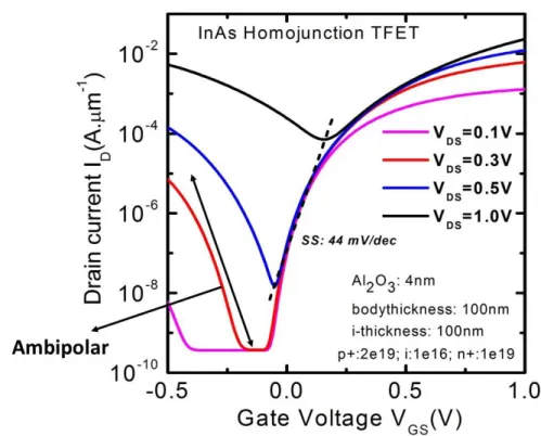
(13) Thèse de Vinay Kumar Chinni, Lille 1, 2017. List of Figures Figure 1: Scaling of transistor over the years following the famous Moore’s law, roughly doubling the number of transistors per chip for every 24 months [2]. ....................... 1 Figure 2: The trend of Power (W/chip) and supply voltage VDD Vs year of a CMOS technology node. (Source: IMEC [4]) ........................................................................ 2 Figure 3: I-V characteristics showing for the MOSFET (blue), TFET (green) in comparison with ideal (orange) I-V characteristics of a transistor................................................. 5 Figure 4: (a) Schematic of a typical I-MOS structure in which the gate only partially covers the right side of the intrinsic region. (b) Transfer characteristics IDS-VGS of Si and heterostructure SiGe I-MOS with a SS of less than 5 mV/dec for left n-channel IMOS and right p-channel I-MOS, where source was biased at 4.8V. The above device schematic and characteristics were taken from [7]. ........................................ 7 Figure 5: (a) Schematic showing the operation of cantilever based 3T NEMS switch with source, drain and gate terminals in the OFF state and ON state taken from [9]. (b) Schematic of 4T relay in OFF and ON states where the gate structure is actuated by VGB and (c) corresponding IDS-VGB of the 4T relay showing SS less than 1mV/decade taken from [11]. ..................................................................................... 8 Figure 6: A conventional FET structure with the gate insulator replaced by a ferroelectric insulator, this means channel see a larger voltage than the actual due to the negative capacitance. Next to the FET structure is the schematic showing the insulator (ferroelectric) capacitor and the semiconductor capacitor connected in series like in a MOSFET. The above picture is taken from [5]. .................................................... 10 Figure 7: (a), (b) Schematic of a three terminal TFET and MOSFET device structure, (c), (d) Scheme showing the barriers that carriers see for a TFET and MOSFET in Off state and (e),(f) Scheme showing the carrier injection mechanism of a TFET and MOSFET in On state [15]. ........................................................................................ 11 Figure 8: (a) Band-to-band-tunneling mechanism under reverse bias and (b) a triangular potential profile [16]. ................................................................................................ 12 Figure 9: Energy band cross section of a TFET showing a triangular barrier [18]. ............. 14 Figure 10: Schematics of heterojunctions. (a) straddling gap (type-I), (b) staggered gap (type-II), and (c) broken gap (type-III). .................................................................... 16 Figure 11: Cross-section schematics of a vertical mesa TFET fabricated by (a) the University of Texas [43], (b)Penn state [25], (c) Intel [30]. In the vertical mesa TFET, the gate is placed on the channel (i) sidewall of an etched mesa. ................. 17 Figure 12: Cross-section schematics of the AlxGa1-xSb/InAs based TFET fabricated at Notre dame University: (a) Air bridge structure with tunneling in-line with the gate field [37], (b) another design with heavily doped drain contact [41]. ...................... 18 Figure 13: Schematics and a SEM image of a fabricated nanowire processed in (a) bottomup approach (nanowire growth) [44], (b) top-down approach (digital dry-etch technique) [45]. Very small diameter has been achieved in both cases, but the quality and processing conditions are yet to be optimized. ...................................... 19 xiii © 2017 Tous droits réservés.. lilliad.univ-lille.fr.
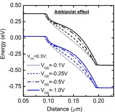
(14) Thèse de Vinay Kumar Chinni, Lille 1, 2017. Figure 14: Cross sectional schematic of a lateral TFET with the source regions formed by ‘Zn’ diffusion developed at (a) the University of Tokyo [28], (b) IMEC [29]......... 20 Figure 15: (a) Schematic of a complementary p-TFET and n-TFET on a common metamorphic buffer and TEM image [54]. (b) Schematic of a C-TFET inverter proposed in the context of the SAMBA project with the selective area epitaxial technology [52]. ........................................................................................................ 23 Figure 16: Device schematic of the double gate n-TFET used in this study. ....................... 26 Figure 17: (a) Flat band profiles for the proposed n-TFET for different ‘Al’ mole fraction of the AlXGa1-XSb/InAs heterojunction. (b) and (c) Energy band diagrams of the InAs/Al0.45Ga0.55Sb heterojunction (Ebeff is 40 meV ) in the OFF and ON states respectively [60]. ...................................................................................................... 27 Figure 18: (a) ID-VDS characteristics, (b) band alignment in reverse bias, (c) equilibrium, (d) peak point (Ip), (e) valley point (Iv), and (f) thermionic diffusion of the InAs homojunction TFET shown in Figure 15. ................................................................. 28 Figure 19: ID-VGS transfer curve of InAs homojunction TFET at a varying VDS. ................ 29 Figure 20: Band profiles showing the ambipolar effect with increasing gate voltage VGS... 30 Figure 21: (a) Simulated Drain current (ID) versus gate voltage (VGS) transfer characteristics of a two-sided gate InAs/AlGaSb Heterojunction TFET with an effective barrier (Ebeff) height of 55 meV and (b) Comparison showing the difference between a homojunction TFET and a heterojunction TFET and how heterojunction boosts ION. .................................................................................................................................. 31 Figure 22: ID-VGS curve for different effective barrier heights (Ebeff) at the InAs/AlXGa1-XSb heterojunction. .......................................................................................................... 32 Figure 23: (a) n-TFET simulated ID-VGS transfer curves for various source doping levels at a constant drain doping of 1 x 1018 cm-3 and (b) n-TFET simulated ID-VGS transfer curves for various drain doping levels at a constant source doping of 1 x 1019 cm-3. .................................................................................................................................. 33 Figure 24: Energy band variations at VGS =-0.25V and VDS = 0.5 V when increasing the source doping level while the drain doping one is kept constant at 1x1018 cm-3. ..... 34 Figure 25: Drain current (ID) versus gate voltage (VGS) transfer characteristics of a vertical two-sided gate InAs/Al0.25Ga0.75Sb Heterojunction TFET at VDS=0.5V with an effective oxide thickness (EOT) of 0.15 nm, 0.43 nm, 0.87 nm and 1.73 nm respectively. For all the devices the gate is aligned to the intrinsic channel thickness of 100 nm and the body thickness is 100nm. ............................................................ 35 Figure 26: n-TFET simulated ID-VGS transfer curves of an InAs/AlGaSb (Ebeff=170 meV) heterojunction TFET comparing the single gate and double gate configurations for two body thickness (Tbody) of 10 nm and 100 nm. .................................................... 36 Figure 27: n-TFET simulated ID-VGS transfer curve for different body thickness (Tbody) of 10 nm, 20 nm, 30 nm, 50 nm and 100 nm respectively while all other parameters of the devices are kept constant. ................................................................................... 37 Figure 28: Simulated energy band diagram at VGS = 1 V and VDS = 0.5 V across the channel, 10nm distance from the gate, for a two-sided gate n-TFET with a Tbody thicknesses of (a) 100 nm and (b) 20 nm respectively. ............................................ 38 xiv © 2017 Tous droits réservés.. lilliad.univ-lille.fr.
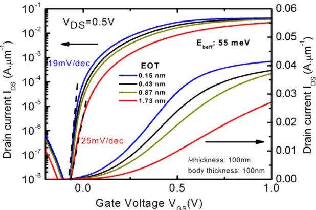
(15) Thèse de Vinay Kumar Chinni, Lille 1, 2017. Figure 29: n-TFET simulated ID-VGS transfer curves of an InAs/AlGaSb (Ebeff: 55meV) heterojunction TFET showing the influence of the intrinsic channel length. ........... 39 Figure 30: Schematic of (a) 40 nm gate underlapped to channel, (b) gate aligned to channel, and (c) 40 nm gate overlapped to drain. ................................................................... 40 Figure 31: (a) n-TFET simulated ID-VGS transfer curves of InAs/AlGaSb heterojunction TFET with different gate alignment with the channel, (b)-(d) Impact on the band profiles under the influence of gate induced electric field at the channel-drain junction. .................................................................................................................... 41 Figure 32: Cross section TEM image of InAs grown on GaSb showing dislocations originating from the interface due to the lattice mismatch between InAs and GaSb. Picture taken from [69]. ............................................................................................ 42 Figure 33: Schematics showing the SRH and TAT leakage mechanisms, taken from [71]. 43 Figure 34: Schematics showing the band-edges and band-tails [74] .................................... 44 Figure 35:Vertical electric field mapping inside the heterostructure for a V-shaped device at VDS=VGS=0.5V (a) or VDS=0.5V and VGS=-1V (c). Vertical electric field mapping inside the heterostructure for a Λ-shaped device at VDS=VGS=0.5V (b) or VDS=0.5V and VGS=-1V (d). The two shapes are reversed and exhibit a width of 80 nm at respectively the source to channel interface (for the V-shape) or channel to drain interface (for the Λ-shape). The band lines-up resulting from this electric field are extracted along a cutline near the InAs/Al2O3 interface (e and g) or along a cutline in the center of the mesa (f and h) for both kind of shape. ....................................... 46 Figure 36: Schematic of the Tunnel Diode and TFET structures used to explain the fabrication process. ................................................................................................... 48 Figure 37: TD process flow cross-sectional schematic. (a) Epitaxial structure. (b) Formation of the top contact. (c) Wet etching of the mesa. (d) Insulating the substrate with SiO2. (e) Contact window opening (via). (f) Bottom contact formation. ................. 50 Figure 38: TFET-EBL mask layout. Top view of the mask showing vertical and horizontal devices of different lengths. ...................................................................................... 51 Figure 39: TFET cross-sectional schematic and process flow steps. ................................... 52 Figure 40: Wet etched mesa profile using PABS solution along the [1-10] direction for a drain contact size of (a) 0.35μm and (b) 1 μm. ......................................................... 53 Figure 41: Wet etched mesa profile using CABS solution along the [1-10] direction for a 0.35μm drain contact size. ........................................................................................ 54 Figure 42: Wet etched mesa profile using PABS + CABS solutions oriented along (a) [110] and (b) [1-10]. ................................................................................................. 55 Figure 43: Wet etched mesa profiles obtained on different heterostructuress achieving a tunnel junction width of (a) 200nm (b) 50nm (c) 60 nm (d) 10nm. ......................... 56 Figure 44: Schematic representation of the atomic layer deposition (ALD) process. By alternating Trimethylaluminum (TMA) and H2O pulses, thin conformal Al2O3 films can be grown with atomic thickness resolution. ....................................................... 57 Figure 45: Dilute ammonia pre-treatment test. (a) SEM image showing the undercut at the tunnel junction. (b) STEM imaging showing the impact of the pre-treatment. ........ 58 Figure 46: Dilute HCl pre-treatment. .................................................................................... 59 xv © 2017 Tous droits réservés.. lilliad.univ-lille.fr.
(16) Thèse de Vinay Kumar Chinni, Lille 1, 2017. Figure 47: Cross-sectional STEM images showing the impact of using a HF solution to etch Al2O3 oxide. (a) Full device and (b) zoom under the gate. ....................................... 59 Figure 48: Process flow of window opening on source and drain areas to etch Al2O3, defined by Electron beam lithography (EBL). (a) Window opening defined by EBL. (b) Plasma etching using BCl3. (c) Lift-off............................................................... 60 Figure 49: Cross-sectional SEM image showing ‘Sb’ based material etch using BCl3 chemistry. .................................................................................................................. 60 Figure 50: (a) Cross-sectional SEM image showing that the gate metal is shorted with the drain contact when the sample is tilted to 600. (b) Top-view SEM image showing the metal residue around the corners of the gate metallization resulted from poorlift-off process. .......................................................................................................... 61 Figure 51: Schematic showing the optimized Process flow to metallize the gate at 600. (a) EBL exposure. (b) Resist Development. (c) Methanol/IPA treatment. (d) Metallization with a 600 tilt (zoom on the device region). ........................................ 62 Figure 52: SEM images of gate metallization for devices oriented in (a) [1-10] and (b) [110] and (c) top view showing the gate metallization and drain. ............................ 63 Figure 53: Cross-sectional STEM image of a fabricated vertical TFET device (a), (c) Ʌshape in [1-10] and (b), (d) V-shape in [110] direction. ........................................... 64 Figure 54: SEM image showing the source contact formation ............................................. 65 Figure 55: SEM images showing the etching of 650nm GaSb buffer using (a) a HF solution (b) a HCl solution and (c) under etching impact. ..................................................... 67 Figure 56: Wet mesa etching of GaSb buffer using a tartaric acid solution. (a), (b) cross section SEM image and (c) top view after mesa isolation. ....................................... 68 Figure 57: SEM images showing the via opening and post exposure bake to fabricate the air bridges. (a) After the EBL exposure without baking. (b) Round corners obtained after baking at 1700C. (c) Round corners at source and drain openings. ................. 69 Figure 58: SEM images showing cracks seen after developing ZEP. (a) Cracks obtained between drain and source. (b) Cracks obtained between drain and gate. ................. 70 Figure 59: (a), (b) and (c) SEM images taken after development of the second bridge lithography level. There are no cracks seen in ZEP with the optimized mask design. .................................................................................................................................. 71 Figure 60: SEM images of (a) channel. (b) Air bridge zoomed at drain contact. (c) Top view of the air-bridge. (d) Tilted view. ..................................................................... 72 Figure 61: Epitaxial structure and band diagram of TD-I. ................................................... 74 Figure 62: Epitaxial structure and band diagram of TD-II. .................................................. 75 Figure 63: Epitaxial structure and band diagram of TD-III. ................................................. 76 Figure 64: Epitaxial structure and band diagram of TD-IV.................................................. 76 Figure 65: (a) I-V curves showing the difference in peak and valley currents, (b) absolute conductance-voltage curves, measured IP (c) and IV (d) versus the tunnel junction area of the epitaxial structures shown in Figure 60-63. ............................................ 78 Figure 66: Epitaxial structure of TD-V and its band diagram generated using Silvaco TCAD tool. ............................................................................................................... 82 Figure 67: (a) I-V characteristics and (b) conductance slope of TD-V. ............................... 83 xvi © 2017 Tous droits réservés.. lilliad.univ-lille.fr.
(17) Thèse de Vinay Kumar Chinni, Lille 1, 2017. Figure 68: Epitaxial structure and band diagram of TFET-I. ............................................... 84 Figure 69: (a) Cross-sectional FIB-STEM image of Ʌ-shaped device fabricated on TFET-I epitaxial layer and (b) IDS-VDS characteristics of device in (a) at different gate voltages (VGS)(Inset: logscale). ................................................................................ 85 Figure 70: Epitaxial structure and band diagram of TFET-II. .............................................. 86 Figure 71: IDS-VDS characteristics of a (a) Ʌ-shaped device and (b) V-shaped device of area 0.25x4 μm2 at different gate voltages (VGS). Inset: FIB-Cross sectional image. ...... 88 Figure 72: (a), (b) IDS-VDS characteristics of the Ʌ-shaped device of area 0.25x2 μm2 and (c), (d) IDS-VDS characteristics of the V-shaped device of area 0.25x2 μm2............. 90 Figure 73: Drain current (ID) variation with the width of the tunnel junction (black curves, left axis) and resulting ratio between the On state and OFF state currents (red curve, right axis). ................................................................................................................. 92 Figure 74: Epitaxial structure and band diagram of TFET-III. ............................................. 93 Figure 75: Plot showing the variation of ION and IOFF w.r.t the width (W) of the tunnel junction for the V-shaped device at VDS=0.5V. ........................................................ 94 Figure 76: 300K IDS-VDS characteristics of the InAs/AlGaSb V-shape TFET in backward (a) and forward regime (b). (c) Transfer characteristics of the device for different VDS and corresponding gate current density, (d) Transconductance curve for VDS=0.5V (black squares) and transfer characteristics for VDS=0.5V in linear scale (red line). ................................................................................................................... 95 Figure 77: (a) Hysteresis observed in the transfer characteristics for the V-shaped device when the gate voltage is swept in two directions at VDS=0.5V. Inset: Top view SEM image showing the gate/source overlap. ................................................................... 96 Figure 78: Low temperature characterization of the device: (a) transfer characteristics versus temperature for VDS=0.1V and (b) Subthreshold slope versus drain current extracted from (a)...................................................................................................... 97 Figure 79 : Arrhenius plot of drain current for VGS=-2.2V showing that the OFF current is dominated at room temperature by a SRH generation-recombination mechanism in InAs (a). For VGS=-1.8V, a Poole-Frenkel (PF) mechanism can be deduced for low VDS (red points) whereas a BTBT phenomenon prevails for large VDS and T<150K (b). For VGS=0.5V (c) and VGS=0V (d), temperature independent drain current evidences a BTBT current domination. .................................................................... 98 Figure 80: 77K characterization of the device: (a) IDS-VDS, (b) transfer characteristics for VDS=0.1V to 0.5V. .................................................................................................... 99 Figure 81: (a) SEM image of 25nm mesa width and (b) FIB-STEM image of 40 nm mesa width defined dry plasma etch technique. .............................................................. 102. xvii © 2017 Tous droits réservés.. lilliad.univ-lille.fr.
(18) Thèse de Vinay Kumar Chinni, Lille 1, 2017. xviii © 2017 Tous droits réservés.. lilliad.univ-lille.fr.
(19) Thèse de Vinay Kumar Chinni, Lille 1, 2017. Abbreviation List ALD. Atomic Layer Deposition. BG. Broken-Gap Semiconductor. BGN. Band Gap Narrowing. BTBT. Band-to-Band Tunneling. CMOS. Complementary Metal Oxide Semiconductor. CNT. Carbon Nano-Tune. CVD. Chemical Vapor Deposition. DC. Direct Current. DOS. Density of States. DI. De-Ionized. EBL. Electron Beam Lithography. EOT. Equivalent Oxide Thickness. FG. Forming Gas. IC. Integrated Circuit. IPA. Isopropyl Alcohol. MBE. Molecular Beam Epitaxy. MOSFET. Metal-Oxide-Semiconductor Field-Effect Transistor. NDR. Negative Differential Resistance. NW. Nanowire. PMMA. Poly (Methyl Methacrylate). PVCR. Peak-to-Valley Current Ratio. RTA. Rapid Thermal Anneal. RIE. Reactive-Ion Etch. SEM. Scanning Electron Microscope. SOI. Silicon-on-Insulator. SRH. Shockley-Read-Hall. SS. Sub-threshold slope. TAT. Trap-Assisted Tunneling. TCAD. Technology Computer-Aided Design xix. © 2017 Tous droits réservés.. lilliad.univ-lille.fr.
(20) Thèse de Vinay Kumar Chinni, Lille 1, 2017. TDD. Threading Dislocation Density. TD. Tunnel diode. TEM. Transmission Electron Microscope. TFET. Tunnel Field-Effect Transistor. WKB. Wentzel-Kramers-Brillouin. xx © 2017 Tous droits réservés.. lilliad.univ-lille.fr.
(21) Thèse de Vinay Kumar Chinni, Lille 1, 2017. Introduction Historically, the most commonly used transistor in integrated circuits (ICs) is the Metal Oxide Semiconductor Field Effect Transistor (MOSFET), based on silicon technology. Complementary MOS (CMOS) circuits use a combination of p-type and n-type MOSFETs to implement digital circuits found in all electronic equipment. The three terminal MOSFET consisting in the gate, drain and source was first fabricated at BELL labs by D. Kahng and M.M. Atalla in 1960 [1] and commercially available in 1964.. Figure 1: Scaling of transistor over the years following the famous Moore’s law, roughly doubling the number of transistors per chip for every 24 months [2].. Scaling of CMOS has achieved an unprecedented success since its invention in 1960 at Bell labs. For more than five decades, MOSFET has been continuously scaled to improve the performances and to add functionalities to the IC. Over the last three decades transistor scaling followed Dennard’s voltage scaling principle, which states that all the device dimensions be scaled by 1/k factor while the doping of source and drain regions increased by a factor k [3]. As a result, MOSFET scaling improved the circuit speed and 1 © 2017 Tous droits réservés.. lilliad.univ-lille.fr.
(22) Thèse de Vinay Kumar Chinni, Lille 1, 2017. density along with the addition of more functionalities. With the scaling progressing at an exponential rate, more and more transistors in a given area have been added lowering the manufacturing cost per transistor. Figure 1 shows this trend. However, an emerging problem associated to the scaling of the supply voltage VDD has appeared. The graph in Figure 2 shows that VDD scaling did not follow the trend of Dennard’s scaling law with the. technology generation node. Indeed, scaling of VDD and of the threshold voltage VTH have adverse effects (decrease of the gate over drive and on the on-state current, decrease of the Ion/Ioff ratio) due to the carrier transport mechanism based on the thermionic emission principle, leading to limitations of the electrostatic control of the gate over the current flow. This non-scaled VDD leads to the power dissipation problem in the recent technology nodes. One way to address this power consumption problem without sacrificing performance is to increase the switching efficiency, which implies a subthreshold slope (SS) of the device steeper than 60 mV/dec at room temperature, which is a physical limit of the conventional MOSFETs.. Figure 2: The trend of Power (W/chip) and supply voltage VDD Vs year of a CMOS technology node. (Source: IMEC [4]). 2 © 2017 Tous droits réservés.. lilliad.univ-lille.fr.
(23) Thèse de Vinay Kumar Chinni, Lille 1, 2017. There are many alternatives to the MOSFETs to achieve steep SS, which are currently studied. The focus of this work will be on one of them: changing the thermionic injection mechanism of charges into the channel by a tunnel injection mechanism independent of the temperature. This is the working principle of the Tunnel Field Effect Transistor (TFET) in which the carrier transport mechanism is fundamentally different from that in MOSFET and for which a SS lower than 60mV/dec can be expected. The realization of a complete transistor involves many parameters and that is why, as a first step, we will investigate tunnel diodes (TDs) to evaluate material properties.. This manuscript is organized along four chapters. Chapter 1 provides the motivation for this work, based on the limitations currently being experienced by the MOSFETs in terms of SS. Possible post-MOSFET devices with lower values of swing are discussed and state-of-the-art on the TFETs fabricated within various material systems and architecture is presented. At the end we present the main objective of this work, which is to realize a vertical n-TFET in the AlGaSb/InAs material system. Chapter 2 presents the operation principles and basic simulation of TFET using the Silvaco software. The parameters such as materials, effective barrier height (Ebeff) at the tunnel junction, doping variations at source and drain, single and double gate configurations, channel body thickness, effective oxide thickness are varied to get a better insight into the device working. Chapter 3 details the fabrication process flow for diodes and TFETs that have been developed entirely in the framework of this study. Chapter 4 discusses the results obtained on the fabricated Tunnel diodes (TDs) and different TFET generations. Finally, the conclusion suggests some recommendations for future work.. 3 © 2017 Tous droits réservés.. lilliad.univ-lille.fr.
(24) Thèse de Vinay Kumar Chinni, Lille 1, 2017. 4 © 2017 Tous droits réservés.. lilliad.univ-lille.fr.
(25) Thèse de Vinay Kumar Chinni, Lille 1, 2017. Chapter 1 – Literature review 1.1 Subthreshold Swing of transistor: CMOS limit The conventional scaling in CMOS technology faced major problems for sub-50nm gate length (Lg), because the operation voltage reduction degrades the sub-threshold leakage current. Figure 3 illustrates that the transition from OFF-state to ON-state is not abrupt and IOFF is not zero in the subthreshold region (VGS < VTH). This leads to a leakage or subthreshold current in the OFF-state. In practice, low VTH is desirable to obtain high ON-current while reducing VDD, but high VTH is needed for low OFF-current. This subthreshold leakage effect slowed down the scaling of the threshold voltage and eventually supply voltage (VDD).. Figure 3: I-V characteristics showing for the MOSFET (blue), TFET (green) in comparison with ideal (orange) I-V characteristics of a transistor.. The subthreshold swing of a MOSFET is defined as the value of the gate voltage (VG) swing needed for one decade change of the drain current (ID), usually expressed in millivolts per decade (mV/dec). In Figure 3, the region below the drain current saturation is called subthreshold region. The subthreshold swing (SS) is the inverse of the subthreshold slope of log (ID) vs VGS and is expressed as [16]:. 5 © 2017 Tous droits réservés.. lilliad.univ-lille.fr.
(26) Thèse de Vinay Kumar Chinni, Lille 1, 2017. 𝑆𝑆 =. 𝐶𝑑𝑒𝑝 𝑑𝑉𝐺 𝑘𝐵 𝑇 = ln(10) (1 + ) 𝑑(𝑙𝑜𝑔10 𝐼𝐷 ) 𝑞 𝐶𝑜𝑥 = (ln(10). (1.1). 𝑘𝐵 𝑇 ) (𝑚) 𝑞. where 𝑘𝐵 is the Boltzmann constant, T is the temperature, Cdep is the depletion capacitance, Cox is the gate oxide capacitance and m is called the body factor. Due to the thermionic nature of the drain current, SS is always limited to 2.3𝑘𝐵 𝑇/𝑞 (=60 mV/decade) at room temperature. Since the SS is purely dependent on the transport mechanism of the carriers in the subthreshold regime, achieving steep SS lower than 60 mV/decade requires changing the way electrons flow in the device. This is the primary motivation behind Impactionization MOSFETS (IMOS), Micro/Nano-Electro-Mechanical FETs (NEMFETs) and Tunnel field effect transistors (TFETs) where the transport mechanism is different from classical silicon based MOSFETs. On the other hand, S. Salahudhin et al. [5] proposed a theory on the negative capacitance to increase the surface potential (m<1) in the channel with respect to what is possible in the MOSFET. 1.2 Alternative small Swing devices: Subthreshold slope below 60mV/decade 1.2.1 Impact-ionization MOSFET (I-MOS) Impact-ionization MOS (I-MOS) is one of the potential electronic device that employs avalanche breakdown to achieve a SS below 10 mV/decade. I-MOS is a gated p+i-n+ structure with a gate partially covering the intrinsic region as shown in Figure 4. Applying a positive gate bias greater than the threshold voltage (Vt) results in an increase of the charge carrier energy. Under the influence of the high electric field the atoms in the lattice are impacted thereby creating more electron-hole pairs. Avalanche breakdown occurs when each carrier produces an electron-hole pair. Since impact-ionization phenomenon is a strong function of the electric field, I-MOS can have a very small subthreshold swing and a high-on current [6].. 6 © 2017 Tous droits réservés.. lilliad.univ-lille.fr.
(27) Thèse de Vinay Kumar Chinni, Lille 1, 2017. (a). (b). Figure 4: (a) Schematic of a typical I-MOS structure in which the gate only partially covers the right side of the intrinsic region. (b) Transfer characteristics I DS-VGS of Si and heterostructure SiGe I-MOS with a SS of less than 5 mV/dec for left n-channel I-MOS and right p-channel I-MOS, where source was biased at 4.8V. The above device schematic and characteristics were taken from [7].. The biggest challenge for the I-MOS is the reduction of the breakdown voltage to enable further scaling of the supply voltage (VDD). Gopalakrishnan et al. proposed the use of low band gap materials such as Ge, to lower the breakdown voltage, but experimental demonstration is still lacking [8]. While the supply voltage of ‘Si’ I-MOS is still higher than for current MOSFETs, Y. Lechaux (Anode group) at IEMN is currently studying III-V based heterojunction I-MOS to lower the supply voltage. Since impact-ionization itself creates hot carriers, this is a matter of concern for repeatability and reliability because hot carriers can go under the gate (into the gate oxide) resulting in threshold voltage shifts and also SS increase of the device. Another major challenge for I-MOS using low band gap materials is the tunneling current. 1.2.2 M/NEMFET (Micro/Nano-Electro-Mechanical FET) Micro/Nano-electro-mechanical. (MEMS/NEMS). relays. utilize. electrostatic. actuation to switch the device from OFF to ON state. The switching behavior is very abrupt and believed to be an excellent choice where the reduction of static power is the main concern. While some MEMS switches are just 2-terminals (2T), which are easy to design 7 © 2017 Tous droits réservés.. lilliad.univ-lille.fr.
(28) Thèse de Vinay Kumar Chinni, Lille 1, 2017. and operate but are limited in terms of applications in circuits, others are 3-terminal (3T) devices. There are many designs available for the 3T relay switch. One of the design is to use a cantilever beam [9] electrostatically “pulled-in” and “pulled-out” as shown in Figure 5 (a). Another possibility is to use a typical MOSFET layout as developed by EPFL. Rhesa et al. [10] developed a 4-Terminal (4T) relay to address the shortcomings of 2T and 3T in circuits [11]. In 4T design as shown in Figure 5 (b), the actuated structure is the gate, whose position is controlled by the applied gate-to-body voltage (VGB), as opposed to the gate-to-source (VGS) in the 3T design.. 3-Terminal (3T) Relay. OFF STATE. ON STATE (a). 4-Terminal (4T) Relay. (b). (c). Figure 5: (a) Schematic showing the operation of cantilever based 3T NEMS switch with source, drain and gate terminals in the OFF state and ON state taken from [9]. (b) Schematic of 4T relay in OFF and ON states where the gate structure is actuated by VGB and (c) corresponding IDS-VGB of the 4T relay showing SS less than 1mV/decade taken from [11]. 8 © 2017 Tous droits réservés.. lilliad.univ-lille.fr.
(29) Thèse de Vinay Kumar Chinni, Lille 1, 2017. MEMS and NEMS are interesting because of their nearly zero leakage current in the OFF state, abrupt SS and very high ION. Their main disadvantages include speed and mechanical reliability where millions of switches should be electrostatically operated thousands or millions of times without failure and also high parasitic capacitance at high frequencies [12]. 1.2.3 Ferroelectric gate dielectric FET Another possibility to reduce the subthreshold swing below 60 mV/decade is by using a ferroelectric insulator in place of the conventional gate oxide insulator [5], because a ferroelectric insulator provides an effective negative capacitance (NC) which allows overcoming the Boltzmann limit. The negative capacitance phenomenon can be explained by considering the first term of the equation (1.1), which is denoted as m. 𝑚 =1+. 𝐶𝐷𝑒𝑝 𝐶𝑖𝑛𝑠. (1.2). The body-factor (m) is always larger than 1 in MOSFETs, because of the voltage divider rule in conventional capacitors. Thus SS cannot be less than 60 mV/decade in MOSFETs. However, if ‘m’ could be made less than one, that will lead to an overall SS less than 60 mV/decade [13]. To achieve this, a negative capacitance insulator (ferroelectric) is connected in series with the semiconductor capacitor as shown in Figure 6. However, these ferroelectric-gate transistors suffer from low field effect mobility and further research has to be conducted [14].. 9 © 2017 Tous droits réservés.. lilliad.univ-lille.fr.
(30) Thèse de Vinay Kumar Chinni, Lille 1, 2017. Figure 6: A conventional FET structure with the gate insulator replaced by a ferroelectric insulator, this means channel see a larger voltage than the actual due to the negative capacitance.. Next to the FET structure is the schematic showing the insulator. (ferroelectric) capacitor and the semiconductor capacitor connected in series like in a MOSFET. The above picture is taken from [5].. 1.3 Introduction to the Tunnel Field effect transistor The tunnel FET also called TFET, is also considered as a potential device for MOSFET replacement for low-power applications. As the carriers tunnel through the barrier, they offer a potential for steep subthreshold swing at a very low OFF state current. Since the tunneling takes place in a very small region of less than 5nm, the gate lengths can be scaled to a distance of tunneling barrier width, which is less than 5nm for III-V materials. The drain current in TFET is independent of the kT/q thermal factor unlike in MOSFET, which makes it possible to achieve subthreshold swing lower than 60 mV/dec. In theory, TFETs make use of band-to-band-tunneling (BTBT) to establish current flow. BTBT of carriers will occur when a heavily doped p-n junction is polarized under reverse bias and the electric field is high enough of the order of 106 V/cm. Under reverse bias, available electrons on the source (p) side tunnel through the narrow barrier and fill the available states in the conduction band of the drain (n) side resulting in a Zener current flow.. 10 © 2017 Tous droits réservés.. lilliad.univ-lille.fr.
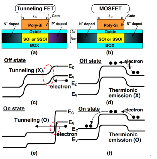
(31) Thèse de Vinay Kumar Chinni, Lille 1, 2017. .. Figure 7: (a), (b) Schematic of a three terminal TFET and MOSFET device structure, (c), (d) Scheme showing the barriers that carriers see for a TFET and MOSFET in Off state and (e),(f) Scheme showing the carrier injection mechanism of a TFET and MOSFET in On state [15].. So, TFETs are gated p+-i-n+ diodes operated in reverse bias with a gate aligned with the intrinsic zone. With almost similar 3-terminals like in an nMOSFET, an nTFET consists of a p+ -region as source, an i-region as channel, and a n+-region acting as the drain. Like in a MOSFET, the gate voltage (VGS) controls the charge in the channel by modulating the height of the barrier. In MOSFETs, charge carriers go over the barrier, while in TFETs they pass through the barrier as shown in Figure 7. When no VGS is applied, the tunneling barrier width is wide enough to impede carrier tunneling: this is the OFF-state. When a positive VGS is applied on the gate, the intrinsic zone bands are pushed down, and the tunneling 11 © 2017 Tous droits réservés.. lilliad.univ-lille.fr.
(32) Thèse de Vinay Kumar Chinni, Lille 1, 2017. barrier width starts to become thinner, thus allowing the majority charge carriers available on the source side to pass through it towards the empty states in the conduction band of the intrinsic zone. As VGS is further increased, the tunneling probability increases which results in a maximum tunneling current, defining the ON state of the TFET. For nTFET, the majority charge carriers are electrons, with the electrons passing from the p+ source to the ichannel and drained through the n+ drain. Conversely, for pTFET, n+ source allows for injection of holes into the channel. Negative VGS and VDS are applied to turn the pTFET ‘ON’. The principle of operation of a TFET is Zener tunneling. As shown in Figure 7 when a VGS is applied to the gate, the channel bands are pushed down, which reduces the tunneling barrier width and thus allowing the tunneling of carriers from source p+ side to the intrinsic region. The tunneling barrier width is the most important parameter that determines the tunneling current i.e. the drain current of the TFET ID. The tunneling of electrons is formally understood by the transmission tunneling probability of electron through a potential barrier. Careful examination of Figure 8(a) indicates that the potential barrier is of triangular shape as shown in Figure 8 (b).. (a). (b). Figure 8: (a) Band-to-band-tunneling mechanism under reverse bias and (b) a triangular potential profile [16].. 12 © 2017 Tous droits réservés.. lilliad.univ-lille.fr.
(33) Thèse de Vinay Kumar Chinni, Lille 1, 2017. The transmission tunneling probability across a triangular potential barrier can be analytically solved using the WKB (Wentzel-Kramers-Brillouin) approximation [17], which is obtained as 4√2𝑚∗. 𝑇𝑡 ≈ 𝑒𝑥𝑝 − (. 3𝑞ћ𝜀. 3 𝐸𝑔2. ). (1.3). where m* is the effective carrier mass, Eg is the band gap of the material, ε is the electric field at the junction. Equation 1.3 is a general expression for BTBT transmission. When it comes to the tunneling transistors, IBTBT (ID) can be obtained with the aid of Figure 9. In a tunneling transistor, at a constant VD and with the increase/decrease of the gate voltage (VG), the energetic difference (Δɸ) between the conduction band on one side and the valence band on the other side decreases/increases along with λ, since the slope of the energy bands are changed under the influence of the gate electric field. The electric field (ε) in Eq. 1.3 can be replaced with (Δɸ + Eg)/λ, which gives 4𝜆√2𝑚∗. 3 𝐸𝑔2. 𝐼𝐵𝑇𝐵𝑇 𝛼 𝑇𝑡 ≈ 𝑒𝑥𝑝 − ( ) 3𝑞ћ(𝛥ɸ + 𝐸𝑔 ). (1.4). Δɸ is the energy window over which tunneling takes place, Eg is the band gap of the material, λ is a tunneling screening length and m* is the effective carrier mass. From the above equation, two important material parameters allow increasing the transmission tunneling probability: a low carrier effective mass and a small semiconductor bandgap.. 13 © 2017 Tous droits réservés.. lilliad.univ-lille.fr.
(34) Thèse de Vinay Kumar Chinni, Lille 1, 2017. Figure 9: Energy band cross section of a TFET showing a triangular barrier [18].. 1.4 TFET State-of-the-art 1.4.1 Material systems 1.4.1a Si/SiGe TFETs The main objective of the TFET is to outperform CMOS transistors in terms of ION at low VDD with SS below 60 mV/decade and a large ION/IOFF ratio. The TFET with sub60mV/decade on Si was first experimentally demonstrated by Choi et al. with an OFFcurrent in the pA/μm range and an ON-current of 12.1 μA/μm [19]. It has been later showed that BTBT current is significantly enhanced by using strained Si [20] and SiGe [21], because the strain induced heterojunction reduces the band gap. Although significant improvements were seen using band gap engineered Si, SiGe [22], high-k metal gate stack, dopant segregated tunneling junctions [23] and nanowire scaling (NW) to improve electrostatics [24], the ON-current (without degrading the OFF-current) values obtained are far from the desired values compared to MOSFETs. The low ON-current in Si is attributed to the large and indirect band gap, which leads to a wide tunneling barrier for the carriers. 1.4.1b III-V TFETs Because of the limitation of Si-based TFETs to achieve large drive currents to compete with CMOS, III-V semiconductors have been considered due to their smaller and direct band gaps, low effective-mass and possibility of band alignment engineering to increase BTBT. To date, there have been many III-V combinations investigated using 14 © 2017 Tous droits réservés.. lilliad.univ-lille.fr.
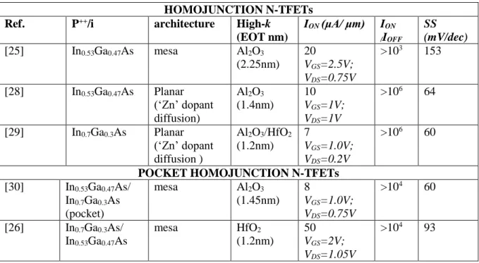
(35) Thèse de Vinay Kumar Chinni, Lille 1, 2017. different architectures. This section reviews the experimental III-V-based TFETs that had been already demonstrated by various groups. Homo-junction TFETs Homojunction TFETs consist of a similar semiconductor material for the source, channel and drain. The most experimentally demonstrated III-V homojunction TFET is based on the InxGa1-xAs ternary alloy with ‘x’ varying from 0.53 to 1 and the corresponding band gap (Eg) from 0.74 eV (x=0.53) to 0.35 eV (x=1). The first In0.53Ga0.47As TFET published by Mookerjea et al. with a vertical mesa structure, achieved an ON-current of 20 μA.μm-1 with a minimum SS (SSmin) of 150mV per decade [25]. Later Zhao et al. improved the ON-current to 50 μA.μm-1 with a SSmin around 90mV per decade by inserting an In0.7Ga0.3As (Eg = 0.59 eV) pocket at the source-channel interface [26], [27]. Recently, Noguchi et al. [28] and Alian et al. [29] achieved a SS of 60 mV per decade on planar InGaAs TFETs, which are the best SS achieved on III-V-based homo-junction TFETs. Table 1 summarizes some of the best experimental results in the literature based on III-V homojunctions. Table 1: III-V-based homojunction N-TFETs. Ref.. P++/i. [25]. In0.53Ga0.47As. [28]. In0.53Ga0.47As. [29]. In0.7Ga0.3As. [30]. In0.53Ga0.47As/ In0.7Ga0.3As (pocket) In0.7Ga0.3As/ In0.53Ga0.47As. [26]. HOMOJUNCTION N-TFETs architecture High-k ION (μA/ μm) (EOT nm) mesa Al2O3 20 (2.25nm) VGS=2.5V; VDS=0.75V Planar Al2O3 10 (‘Zn’ dopant (1.4nm) VGS=1V; diffusion) VDS=1V Planar Al2O3/HfO2 7 (‘Zn’ dopant (1.2nm) VGS=1.0V; diffusion ) VDS=0.2V POCKET HOMOJUNCTION N-TFETs mesa Al2O3 8 (1.45nm) VGS=1.0V; VDS=0.75V mesa HfO2 50 (1.2nm) VGS=2V; VDS=1.05V. ION /IOFF >103. SS (mV/dec) 153. >106. 64. >106. 60. >104. 60. >104. 93. 15 © 2017 Tous droits réservés.. lilliad.univ-lille.fr.
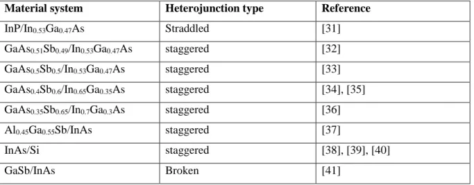
(36) Thèse de Vinay Kumar Chinni, Lille 1, 2017. From the Table 1, it is noteworthy that a thin intrinsic In0.7Ga0.3As as a pocket improves the tunneling probability and also SS compared to the homojunction TFET. Although, III-V homojunction TFETs with pockets exhibit lower SS and higher drive current compared to Si or even SiGe, the drive current has to be further improved to compete with standard CMOS. Hetero-junction TFETs Another strategy to further increase the ON-current is to use a heterostructure at the tunneling junction. Heterojunction, where the source material is different from the channel and drain, allows for a variety of tunnel barriers to be engineered. There are three types of band alignments possible with the heterojunction: Straddling gap (type I), staggered gap (type II) and broken gap (type III) (Figure 10). Different types of heterojunction TFETs fabricated by various groups are highlighted in Table 2. (a). (c). (b). Figure 10: Schematics of heterojunctions. (a) straddling gap (type-I), (b) staggered gap (type-II), and (c) broken gap (type-III).. Table 2: Types of Heterojunction band alignments formed using various material systems Material system. Heterojunction type. Reference. InP/In0.53Ga0.47As. Straddled. [31]. GaAs0.51Sb0.49/In0.53Ga0.47As. staggered. [32]. GaAs0.5Sb0.5/In0.53Ga0.47As. staggered. [33]. GaAs0.4Sb0.6/In0.65Ga0.35As. staggered. [34], [35]. GaAs0.35Sb0.65/In0.7Ga0.3As. staggered. [36]. Al0.45Ga0.55Sb/InAs. staggered. [37]. InAs/Si. staggered. [38], [39], [40]. GaSb/InAs. Broken. [41]. 16 © 2017 Tous droits réservés.. lilliad.univ-lille.fr.
(37) Thèse de Vinay Kumar Chinni, Lille 1, 2017. 1.4.2 TFET Device architectures Like for any other device, the electrical characteristics differ widely by the architecture and the fabrication methodologies used for the fabrication of TFETs. 1.4.2a Vertical mesa Vertical mesa design utilizes dry etching or wet chemical etching [27] or even both to define the channel mesa [25]. A single gate or a two-sided gate is placed on the mesa sidewall as shown in the schematics of Figure 11 to modulate the carriers inside the channel. In the vertical mesa design, the off-state leakage is caused by a Schockley-ReadHall generation-recombination current, so Mookerjea et al. proposed to scale the mesa dimensions to reduce the effect of defects in reverse bias [42].. (a). (b). (c). Figure 11: Cross-section schematics of a vertical mesa TFET fabricated by (a) the University of Texas [43], (b)Penn state [25], (c) Intel [30]. In the vertical mesa TFET, the gate is placed on the channel (i) sidewall of an etched mesa. The main challenge for the fabrication of vertical mesa TFETs is to perfectly align the gate on the channel region. The gate overlap or underlap can result in a reduced electrostatic control of the charges in the channel. 17 © 2017 Tous droits réservés.. lilliad.univ-lille.fr.
(38) Thèse de Vinay Kumar Chinni, Lille 1, 2017. 1.4.2b TFETs with Tunneling Normal to the Gate The University of Notre dame demonstrated a TFET with the gate electric field aligned to the tunneling direction. In this design a very thin top epitaxial layer is grown forming the drain and channel. The gate is placed on top of the n+ drain layer to modulate the tunneling junction. The source is then selectively wet etched to separate the source and the channel forming an air bridge underneath the channel as shown in Figure 12 (a). While the tunneling current maybe enhanced, this design has several disadvantages. There is a significant series resistance inherent to the design [37]. In order to mitigate the series resistance impact, another design named gate recess process (see Figure 12 (b)), demonstrated by Notre dame, involves a higher doped drain layer under the drain contact [41]. This approach achieved a record ON state-current of 180 μA/μm, however the SS is still limited by the interface trap density (Dit) at the oxide/semiconductor interface and trapassisted tunneling (TAT) at the tunneling junction. Moreover, this architecture does not allow easy gate down scaling.. (a). (b). Figure 12: Cross-section schematics of the AlxGa1-xSb/InAs based TFET fabricated at Notre dame University: (a) Air bridge structure with tunneling in-line with the gate field [37], (b) another design with heavily doped drain contact [41]. 18 © 2017 Tous droits réservés.. lilliad.univ-lille.fr.
(39) Thèse de Vinay Kumar Chinni, Lille 1, 2017. 1.4.2c Nanowire TFETs The vertical nanowire is an ideal geometry for TFET application since a wrapped gate-all-around (GAA) cylindrical nanowire channel allows the best electrostatic control of the carriers. The cross-section schematic of a recently fabricated vertical nanowire heterojunction TFET is shown in Figure 13. Nanowires are formed either by nanowiregrowth assisted by a catalyst [44], [39] or top-down approach using the digital dry etch technique [45].. (b). Figure 13: Schematics and a SEM image of a fabricated nanowire processed in (a) bottomup approach (nanowire growth) [44], (b) top-down approach (digital dry-etch technique) [45]. Very small diameter has been achieved in both cases, but the quality and processing conditions are yet to be optimized.. Both approaches exhibited an improved SS compared to the vertical mesa architecture because of the aggressively scaled dimensions. But from a manufacturing stand point the digital dry etch approach may be easier than the nanowire growth since the existing plasma tools in the industry can be easily adapted to the dry etch processing.. 19 © 2017 Tous droits réservés.. lilliad.univ-lille.fr.
(40) Thèse de Vinay Kumar Chinni, Lille 1, 2017. 1.4.2d Lateral TFETs From a cross-sectional point of view, the lateral TFET architecture is almost similar to the classical MOSFET ones due to its planar nature. For the InGaAs TFET fabricated by Noguchi et al. the source (p+) is formed by Zn-diffusion to form the defect-less p+/i tunnel junction [28]. With extremely steep doping profiles and a good quality tunneling interface, trap-assisted tunneling (TAT) is reduced which results in a steep SS. Figure 14 shows a schematic of the lateral TFET fabricated at the University of Tokyo and IMEC.. (a). (b). Figure 14: Cross sectional schematic of a lateral TFET with the source regions formed by ‘Zn’ diffusion developed at (a) the University of Tokyo [28], (b) IMEC [29].. 1.4.3 Overview of Heterojunction TFETs Table 3 shows that several heterojunction TFETs achieve a large ON state current over a gate swing of 0.5 V. The large ON state current, however, appeared at the stake of the ION/IOFF ratio. While the GaSb/InAs (Sb) material system is the best performing so far in terms of high ON state current at VDS=0.5 V, it exhibits an ION/IOFF ratio less than 103 in all 20 © 2017 Tous droits réservés.. lilliad.univ-lille.fr.
(41) Thèse de Vinay Kumar Chinni, Lille 1, 2017. the cases. The absence of steep SS less than 60 mV/dec is noteworthy, except in the work from Tomioka et al.[40] and is typically attributed to the high Dit at the semiconductorchannel/oxide interface and trap-assisted-tunneling (TAT). Mookerjea et al. reported that continued reduction of the mesa area and effective oxide thickness (EOT) can reduce the leakage effects and improve the SS [42]. This statement is confirmed in the case of nanowires: indeed Zhao et al. [45] and Memisevic et al. [44] fabricated a thin nanowire TFET with a diameter less than 20nm in two different approaches and achieved a SS close to 60 mV per decade. However, the ON state current is lower in this case. The experimental results show that further EOT and body thickness scaling within the InAs/AlxGa1-xSb material system allows for further improvement of the ON state current and lower SS and offers a promising perspective for replacing CMOS.. Table 3: Heterojunction TFETs. Ref. [46]. [47]. [41]. [48]. [34]. [49]. [35]. HETEOJUNCTION N-TFETs architecture High-k ION (μA/ μm) (EOT nm) InP/InxGa1-xAs Al2O3/HfO2 20 (x->1.0-0.53) (1.3nm) VGS=1V; VDS=0.5V Al0.4Ga0.6Sb/InAs Al2O3/HfO2 78 (1.6nm) VGS=0.5V; VDS=0.5V GaSb/InAs Al2O3/HfO2 180 (1.3nm) VGS=0.5V; VDS=0.5V GaSb/AlSb/InAs 10nm16 (quantum well) ZrO2 VGS=0.4V; VDS=0.4V GaAs0.35Sb0.65/ Mesa Al2O3/HfO2 135 In0.7Ga0.3As (1.75nm) VGS=2.0V; (High HetroJ) VDS=0.5V GaAs0.18Sb0.82/In0.9Ga mesa Al2O3/HfO2 740 (2nm) VGS=2.0V; 0.1As VDS=0.5V GaAs0.4Sb0.6/In0.65Ga0 mesa HfO2 130 (1.2nm) VGS=2.0V; .35As VDS=0.5V NANOWIRE HETEROJUNCTION N-TFETs diameter P++/i. ION/IOFF >106. SSmin (mV/dec) 93. >103. 125. >103. 200. 103. 194. >104. 169. 102. >500. >105. 105. 21 © 2017 Tous droits réservés.. lilliad.univ-lille.fr.
(42) Thèse de Vinay Kumar Chinni, Lille 1, 2017. [45]. InGaAs/InAs. [50]. GaSb/InAs (Sb). [51]. GaSb/InAs. [44]. GaSb/InAs. [40]. Si/InAs. 50nm (top-down approach) 70nm (bottom-up approach) 45nm (bottom-up approach) 20nm (bottom-up approach) 30nm (bottom-up approach). Al2O3 (1.2nm) Al2O3 (1.3nm) Al2O3/HfO2 (1.4nm) Al2O3/HfO2 (1.4nm) Hf0.8Al0.2Ox (1.4nm). 0.27 VGS=0.3V; VDS=0.3V 140 VGS=0.3V; VDS=0.5V 5 VGS=0.5V; VDS=0.5V 35 VGS=0.5V; VDS=0.5V 1 VGS=0.5V; VDS=1.0V. >102. 75. 102. 320. 102. 130. >102. 68. >106. 21. 1.4.4 Complementary TFETs While heterostructure TFETs offer the best alternative possibility for logic applications, the demonstration of low SS p-TFET integration results are lagging. Many challenges exist for the integration of complimentary TFET (C-TFET) on a ‘Si’ platform. Selective area growth epitaxial technology [52] or nanowire template growth [53] could be possible solutions to realize C-TFET on the same wafer. Recently, Pandey et al. demonstrated record performance of n-TFET and p-TFET on the same material system as shown in Figure 15 (a) [54] for the InGaAs/GaAsSb material system. Similar approach has been proposed within the ‘6.1Å’ family in the context of the ANR Samba project (Figure 15(b)).. 22 © 2017 Tous droits réservés.. lilliad.univ-lille.fr.
(43) Thèse de Vinay Kumar Chinni, Lille 1, 2017. (b). Figure 15: (a) Schematic of a complementary p-TFET and n-TFET on a common metamorphic buffer and TEM image [54]. (b) Schematic of a C-TFET inverter proposed in the context of the SAMBA project with the selective area epitaxial technology [52].. 1.5. Conclusion This chapter presented the reasons for searching small swing switches. The most important one is the continuous increase of power consumption in conventional CMOS technology. In this first chapter we have presented the most promising devices that are 23 © 2017 Tous droits réservés.. lilliad.univ-lille.fr.
(44) Thèse de Vinay Kumar Chinni, Lille 1, 2017. widely investigated. Among them, the tunnel field-effect transistor relies on the tunnel injection of carriers through the band gap at the source/channel interface. This mechanism being independent on the operating temperature, the TFET is a potential candidate for ultralow supply voltage (less than 0.5 V) electronics. The state-of-the art of TFET shows that, although Si or Ge-based devices can achieve a SS lower than 60 mV/dec, the related ION current is still too low to fulfill the requirements of the CMOS technology. This has led to the use of III-V-based small band gap homojunctions and heterojunctions, which can offer much larger tunneling probabilities. Considering heterojunction TFETS, high ON currents can be easily achieved in the GaSb/InAs broken gap material system, but this goes along with high OFF currents. For this reason, the (Al)GaSb/InAs(Sb) heterostructure is very attractive as the band offset can be tuned from type II (staggered gap) to type III (broken gap). The results so far on the AlGaSb/InAs material system are based on a lateral architecture. However, to achieve a good electrostatic control, a vertical architecture is highly desirable. Therefore, in this work we will focus on the fabrication of a vertical device with side gates based on the type II (Al)GaSb/InAs material system.. 24 © 2017 Tous droits réservés.. lilliad.univ-lille.fr.
(45) Thèse de Vinay Kumar Chinni, Lille 1, 2017. Chapter 2: N-TFET device design and optimization In the previous chapter, we have explained the working principle of TFETs and compared the experimental results available in the literature. It has been concluded that heterojunction TFETs based on (near) broken gap heterojunctions such as AlxGa1-xSb/InAs enhance the tunneling current. In this chapter, we will design and discuss various design parameters about the n-TFET device within the AlxGa1-xSb/InAs material system with the help of the Silvaco Atlas simulator. In this work, we use a Band-to-Band Tunneling (BTBT) model because the drive current in n-TFETs is determined by the amount of carriers that tunnel from the source side (p+) valence band to the channel side (i) conduction band. The BTBT model is based on the Wentzel-Kramers-Brillouin (W.K.B) approximation available in the commercial Silvaco TCAD software [55]. At first, the basic TFET design used in this simulation is explained and the importance of using a heterojunction in terms of high ION/IOFF ratio is highlighted. The simulation parameters have been separated in two different categories:. material. properties and device geometry. Finally, we discuss the possible challenges and performance limitations in practical heterojunction TFETs. The cross sectional n-TFET configuration studied in this chapter is shown in Figure 16. In an n-TFET device, p+ acts as a source, i and n+ act as the channel and drain respectively. In the material engineering section, the influence of the source and drain doping and that of the effective barrier height (Ebeff) at the junction are presented. In the geometrical engineering section, the gate dielectric and the channel body thickness (W or Tbody) as well as the channel length (L) and the gate alignment parameters are discussed.. 25 © 2017 Tous droits réservés.. lilliad.univ-lille.fr.
Figure
![Figure 5: (a) Schematic showing the operation of cantilever based 3T NEMS switch with source, drain and gate terminals in the OFF state and ON state taken from [9]](https://thumb-eu.123doks.com/thumbv2/123doknet/3695884.109764/28.918.146.821.423.909/figure-schematic-showing-operation-cantilever-switch-source-terminals.webp)
+7
![Figure 11: Cross-section schematics of a vertical mesa TFET fabricated by (a) the University of Texas [43], (b)Penn state [25], (c) Intel [30]](https://thumb-eu.123doks.com/thumbv2/123doknet/3695884.109764/37.918.150.815.461.895/figure-cross-section-schematics-vertical-fabricated-university-texas.webp)
Documents relatifs
L’archive ouverte pluridisciplinaire HAL, est destinée au dépôt et à la diffusion de documents scientifiques de niveau recherche, publiés ou non, émanant des
Characterization of the pentacene thin-film transistors with an epoxy resin-based polymeric gate insulator.. Chang Hyun Kim, Denis Tondelier, Bernard Geffroy, Yvan Bonnassieux,
Drain current vs gate voltage characteristics of two bulk NMOS transistors: an Open Layout Transistor (OLT, top, a) and an Enclosed Layout Transistor (ELT, bottom, b) before
Exprimer le gain en tension de l'étage grille commune v o /v i2 et sa résistance d'entrée R i2 en fonction de g m2 , χ et R ( en considèrera r 02 la résistance de sortie de Mn2
،لﺎﻤﺸ ءﺎﻨﻴﺴ 2015 ( كوﺒﺴﻴﺎﻔﻝا ﻲﻋﺎﻤﺘﺠﻻا لﺼاوﺘﻝا ﻊﻗوﻤﻝ بادﻵا ﺔﻴﻠﻜ ﺔﺒﻠط مادﺨﺘﺴا لوﺤ : و تﺎﻫﺎﺠﺘﻻا تﺎﻗوﻌﻤﻝا. ﻰﻠﻋ ﻪﻌﻴزوﺘ مﺘ و ﺔﻴﺴﻴﺌر ةادﺄﻜ نﺎﻴﺒﺘﺴﻻا ﻰﻠﻋ ثﺤﺒﻝا اذﻫ ﻲﻓ دﺎﻤﺘﻋﻻا
I suggest that an intention is a complex state in which a predominant desire toward a plan is not inhibited by a gate mechanism whose function is to assess the comparison of our
Vertical Silicon Nanowire Field Effect Transistors with Nanoscale Gate-All-Around.. Youssouf Guerfi,
Now we turn to the idealized (long range) ordering structure. On basis of the ordering and antiordering vec- tors, extracted from the pair correlation function, we derive the
