HAL Id: hal-02974129
https://hal.archives-ouvertes.fr/hal-02974129
Submitted on 21 Oct 2020HAL is a multi-disciplinary open access archive for the deposit and dissemination of sci-entific research documents, whether they are pub-lished or not. The documents may come from teaching and research institutions in France or abroad, or from public or private research centers.
L’archive ouverte pluridisciplinaire HAL, est destinée au dépôt et à la diffusion de documents scientifiques de niveau recherche, publiés ou non, émanant des établissements d’enseignement et de recherche français ou étrangers, des laboratoires publics ou privés.
Methylated Silica Surfaces Having Tapered
Nipple-Dimple Nano-pillar Morphologies as Robust
Broad-Angle and Broadband Anti-Reflection Coatings
Mehrnaz Modaresialam, Jean-Benoît Claude, David Grosso, Marco Abbarchi
To cite this version:
Mehrnaz Modaresialam, Jean-Benoît Claude, David Grosso, Marco Abbarchi. Methylated Silica Sur-faces Having Tapered Nipple- Dimple Nano-pillar Morphologies as Robust Angle and Broad-band Anti-Reflection Coatings. ACS Applied Nano Materials, American Chemical Society, 2020. �hal-02974129�
Methylated Silica Surfaces Having Tapered
Nipple-Dimple Nano-pillar Morphologies as Robust
Broad-Angle and Broadband Anti-Reflection Coatings
Mehrnaz Modaresialam1, Jean-Benoît Claude1, David Grosso1*, and Marco Abbarchi1*
1Aix Marseille Université, Université de Toulon, CNRS, IM2NP Marseille, France
KEYWORDS: Anti-reflection Coating, Sol-gel methylated silica, Nano imprint lithography, nipple-dimple structure, mechanical resistance, chemical resistance, thermal resistance,
ABSTRACT: In this work, mechanically, chemically and thermally resistant broad-band and broad-angle anti-reflection coatings were prepared on 10 cm diameter glass substrates combining sol-gel deposition with nano-imprint lithography. The coatings are composed of water-repellent methylated silica (Si4O7Me2) and exhibit a transverse refractive index gradient created by tapered,
nipple-dimple, sub-wavelength nano-structures, featuring a record vertical aspect ratio of ~1.7. The structure is composed of hexagonal arrays of nano-pillars (~200 nm height; ~120 nm width) and holes (~50 nm depth, ~100 nm width) with 270 nm pitch. The corresponding effective refractive index is between 1.2 and 1.26 depending on the fabrication conditions. Total transmission for double-face nano-imprint wafers reaches 96~97% in the visible range, it is limited by specular reflection and mostly by the intrinsic diffusion of the glass substrate. The anti-reflective effect is effective up to ~60 degrees incidence angle. We address the robustness of the inorganic-based coating in various realistic and extreme conditions comparing them to the organic Perfluoropolyether (PFPE) counterpart (master reference). The sol-gel system is extremely stable at high temperature (up to 600°C, against 200°C for the polymer reference). Both systems showed excellent chemical stability, except in strongly alkaline conditions. The inorganic nano-structure showed abrasion resistance more than two orders of magnitude superior to the polymer one, with less than 20% loss of anti-reflective performance after 2000 rubbing cycles under ~2 Ncm-2 pressure. This difference springs from the large elastic modulus of the
sol-gel material combined with an excellent adhesion to the substrate and to the specific nipple-dimple conformation. The presence of holes allows maintaining a refractive index gradient profile even after tearing-out part of the nano-pillars population. Our results are relevant to applications where transparent windows with broad-band and broad angle transmission are needed, such as protective glasses on photovoltaic cells or C-MOS cameras.
Introduction
Efficient Anti-Reflection Coatings (ARC) have been extensively studied and are nowadays well established in industrial applications over large scales (e.g. for photovoltaic, opto-electronic devices, laser windows and much more).1,2,3 ,4,5 ARC-based multilayered thin films, refractive
index gradient and surface texturing with micro/nano structures have been optimized with many different methods. Beyond optical performances (e.g. improved transmission over a broad
spectral band and a broad acceptance angle), there are several features, such as ease of implementation over large scales, mechanical, thermal and chemical stability, rendering an ARC a competitive device that are not commonly addressed in most reported works. 6,7,8,9
Most common ARC are two-dimensional layers. Their working principle is destructive interference of reflected and impinging light. This kind of 2D ARC are extremely well developed thanks to the ease of implementation, cost-effectiveness, and hydrophobicity.10 However, owing
to the underlying working principle, they can be optimized only for a specific angle, limiting their performances in applications where the incidence of the impinging light beam can change (e.g. in photovoltaic). 1,3 This is why advanced nano-fabrication techniques were developed in order to
produce ordered and disordered 3D sub-micrometric structures extending the performances of ARC to larger angles. In addition, the presence of such 3D structures is extremely useful to suppress interference and thus spectral and angular dependence of their optical properties. These structures can exploit resonance effects of high-permittivity particles (e.g. dielectric-based such as Si11,12 Ge13 and TiO
214,15, or metallic-based, such as Au resonators16). Other materials featuring
a lower dielectric constant (such as polymers and silica) have been used to produce a refractive index gradient on glass, providing an adiabatic change of optical constant from air (n = 1) to the underlying material (e. g. n ~ 1.5 for glass)17,18. For this latter working principle, the effective
refractive index of the graded layer should be close to the square root of the substrate one (Fresnel’s law). If the substrate is glass, materials that are non-absorbing at visible frequencies and exhibit intrinsic refractive index of typically between 1.37 and 1.70 are used in combination with void. The 3D structures must be composed of features having dimension and pitch much below the wavelength of the impinging visible radiation (typical size ~100 nm) to prevent scattering and diffraction, and have a large vertical to horizontal size aspect ratio. These features render their implementation challenging.
Ideal moldable materials gathering all the required properties can be found in organic polymers. They can be processed with high throughput soft-nano imprint lithography (NIL) methods19,20,21, 22, 23 that consist in imprinting the soft-viscous material with an elastomeric stamp before
consolidation. 3D micro- and nano-structures made of thermoplastic organic polymers, such as PMMA, have been elaborated on a plethora of substrates. However, 3D structures made of plastic are mechanically fragile with respect to flat, dielectric layers. As such, they do not provide the longevity necessary for instance, for integration onto photovoltaic panels (~20 years). Moreover, polymers are not very resistant to photo bleaching and high temperature rendering them more prone to deterioration. Furthermore, the detrimental impact of micro- and nano-plastic on the environment and their potential damage to human health demands for a drastic reduction to the use of these materials.
Alternatively, 3D nanostructures have been elaborated in hybrid (organic/inorganic) 24, 25, 26 silica
through direct sol-gel NIL processs27 over relatively small glass wafers. They showed a
remarkable reduction of reflection up to an acceptance angle of 60 degrees.28 These results
account for the relevance of this approach, however, mechanical, thermal and chemical stability have not yet been properly addressed so far and the extension of the printed areas is still limited.
The present work is dedicated to the elaboration and the complete characterization of sol-gel nano-imprinted methylated silica (Si4O7Me2) nanostructures as efficient graded ARC on glass.
The imprint was performed by using a PDMS mold that was replicated from a commercial nipple-dimple Perfluoropolyether (PFPE) ARC master that is systematically used as a reference for comparing the performances of our methylated silica ARC. We first demonstrate the possibility to process sol-gel ARCs composed of nano-metric structures obtained by NIL over the record size of 10 cm diameter wafers (which is the maximal size of the available PDMS mold), confirming the scalability and the cost-effectiveness of the method. Overall, the sol-gel replica exhibited superior ARC performances and stability than the initial polymer counterpart. Indeed, the presence of the graded sol-gel ARC, with calculated effective refractive index of ~1.27, improves the total transmission of visible light of about 6-7% with respect to the bare glass substrate, which is 1% better than the polymer master ARC. Finally, both organic and inorganic coatings showed excellent chemical stability, while the inorganic one was much more resistant to abrasion and high temperature. Indeed, the nipple-dimple conformation allowed preserving the AR properties even after 2000 rubbing cycles for the sol-gel system. These results confirmed that, due to their processability, the versatility to adjust their optical constants, and their robustness, sol-gel materials are ideal systems to serve as nanostructured ARC over large surfaces.
Results
Thin methylated silica (Si4O7Me2) ARC coatings were elaborated on 10 cm wafers as detailed in
the method section. The Si4O7Me2 composition has been selected for its relatively low refractive
index and hydrophobicity, as shown in previous study.10 Structural and optical characteristics of
the graded coating are given in Figure 1. First, the visual inspection of the coating revealed a slight diffused blue color all over the 10 cm coating if one observes at high incident angles (Figure 1A), originating from the diffraction of the nano-pillars array. Since this aspect is found all over the coating, one can state that the whole surface is homogeneously structured. A more accurate description of the 3D structure of the surface has been deduced from SEM micrographs acquired in various configuration (Figure 1C, E, F, G). They revealed the expected nipple-dimple structure faithfully replicated from the perfluoropolyether ARC master. The structure is composed of intercalated hexagonal arrays of pillars and holes separated by a pitch of 270 nm. The pillars (nipples) have ~200 nm height and ~120 nm width, while the holes (dimples) are ~50 nm deep and ~100 nm width. Note that, previous reports on NIL of silica-based sol-gel coatings did not provide pillars featuring such a large vertical aspect ratio 29 28 nor a nipple-dimple
structure. Both characteristics are important to produce a smoother change of refractive index. The thickness and refractive index of the non-imprinted bare layer were 480 nm and 1.33 at a wavelength of 600 nm, respectively (measured by ellipsometry on a flat layer, not shown ).
Figure 1. A) Picture of 10 cm diameter wafer coated with the nanoimprinted methylated silica (Si4O7Me2)
antireflection coating (MS ARC). B) Scheme illustrating the topography of the nipple-dimple surface. C) Scanning electron microscopy (SEM) image of MS ARC the patterned surface (tilted at 52 degree). D) Refractive index profile of the MS ARC system deduced from the structure geometry. E) to F) SEM images of the MS ARC from the top (E), from the side after FIB-preparation (F), and from a 52° tilted angle (G) Typical dimensions of the structure have been measured on SEM images (E, F, G) and are reported in each image for clarity. These have been used to calculate the volume fraction transversal profile of the ARC, from which the refractive index profile (D) was deduced using a linear medium approximation (S1, S2 correspond to projected surface of the nipple and dimple, respectively, modeled using 2 half circles sandwiching a rectangle).
Since silica has a refractive index around 1.5, the measured value of n = 1.33 suggests that the layer has a residual porosity P of around 33% vol. By taking into account these optical and structural features, we deduce the transverse profile of void-to-material volume fraction, the corresponding refractive index profile and the global effective refractive index (neff). The plot
shown in Figure 1 D) reports this profile assuming a linear effective medium approximation. The coating is thus composed of three layers: the non-imprinted pristine material at the bottom (nbot =
1.33, hbot = 350 nm), the layer bearing holes in the middle (nmid = 1.21, hmid = 50 nm), and the top
layer composed of pillars (ntop = 1.13, htop = 150 nm). Assuming a simplified geometry of the
structure, the refractive index profile has been slightly smoothed at the top and bottom edges in order to better reproduce the edge shapes observed in the real structures. The resulting calculated effective refractive index is neff = 1.27 at 600 nm.
Optical performance
Changing the initial sol-gel layer thickness and its intrinsic refractive index will result in a different neff and different ARC properties. Here, the refractive index is fixed by the material
composition (Si4O7Me2), while the thickness of the layer has not been optimized.
Spectra in Figure 2 A) and B) compare the transmission and diffusion of Si4O7Me2 sol-gel layers
(plain non-imprinted, single-face sol-gel ARC imprinted, double-face sol-gel ARC imprinted) with those of the bare glass substrate and of the polymer master ARC (all substrates are from the same producer batch). All spectra in Figure 2 A) and B) were collected at quasi-normal incidence (12 degrees) using a spectrophotometer mounting an integrating sphere allowing to measure the spectral features of total reflection, reflected diffusion (that is total reflection minus specular reflection) and total transmission. Absorption can be excluded in the investigate range of wavelength for both the substrate and the sol-gel coatings in use. The transmitted intensity is larger for nanostructured MS ARC and spectrally flatter with respect to the plain sol-gel, confirming the superior performances of graded systems (Figure 2A). The single-face sol-gel MS ARC allows for a transmission increase of 3% with respect to the bare glass substrate, which is 1% above the PFPE graded counterpart Polymer ARC. This improved transmission property is likely due to a lower neff of the sol-gel layer compared to that of the polymer. A double-face
imprinted Si4O7Me2 sol-gel (MS ARC DF) shows a rather flat transmission of 96%-97% over the
full visible spectrum. It is limited by specular reflection and reflected diffusion. Measuring the reflected scattering allows to assess the haze of the structure, that is an important parameter for using these devices in transmission (Figure 2B). It emerges that bare glass scatters almost 3% of the impinging light, that is very similar to the plain (not imprinted) Si4O7Me2 coated glass,
scattering about 3%. This accounts for the high quality in terms of homogeneity and flatness of our sol-gel coatings. From the same analysis on 3D NIL structures (Figure 2B) we observe that the Polymer ARC scatters about 4-4.5% of the impinging light, whereas the MS ARC is in the 3-4% range demonstrating a reduced haze in our inorganic material with respect to the organic counterpart. Provided flat layers scatters only ~3% of the light, we deduce that the diffusion from the nipple-dimple structure in MS ARC is about 1-2%. This also suggests that the intrinsic scattering from the underlying glass support is actually the main limiting factor for light transmission of the double face ARC shown in Figure 2 A).
Figure 2. A) Total transmission spectra of single face NIL Methylated silica antireflection coating (MS ARC, green full curve), double-face NIL Methylated silica antireflection coating (MS ARC DF, green dashed curve), polymer ARC (blue curve), flat Methylated silica coating 480 nm thick (Plain, red curve) and bare glass (Glass, black curve). Symbols represent the theoretical prediction for a single layer of 120 nm with n = 1.225 (Sim. SQRT) and a composite layer (Sim. Comp.) composed by “bulk” sol-gel bottom layer (nbot = 1.33, hbot = 350 nm), the dimple middle layer (nmid = 1.21, hmid = 50 nm) and the nipple top layer
(ntop = 1.13, htop = 150 nm). B) Normalized diffusion spectra of samples MS ARC, Polymer ARC, Plain and
Glass. C) Scheme of the experimental setup for detecting the specular reflection. The angle of incidence of the illumination light beam (θillumination) and that of the detection (θdetection) are the same. D) Angle-resolved
specular reflection normalized to the reflection of the bare glass substrate (black dashed line, corresponding to MS ARC (green line), polymer ARC (blue line), MS (methylated silica) plain surface thin film (red line).
These performances in transmission are in line with those reported for double-side coated graded ARC systems30,31,32,33. A graded ARC from a similar sol-gel hybrid material was reported28,
exhibiting an excellent ARC effect close to 0% in reflection (at ~560 nm) with a fluctuation of ~3% in the full visible range. Although no data for transmission were provided, the very low reflection for the double-coated system is likely due to the use of a high-quality, non-diffusive substrate, combined with the presence of nanostructures that provides a lower effective refractive index (neff = 1.20).28
We trace the theoretical predictions (obtained with a transfer matrix method) for maximal transmission with single and multi-layered, double face ARC (Figure 2 A, gray curves). One case refers to 120 nm thick layer having n ~ 1.225 (close to the square root of the refractive index of the underlying glass substrate), matching the condition of maximal transmission at about 600 nm. The corresponding curve is rather flat and the fluctuation, in the considered spectral range, is less than 2%. The second simulation takes into account a more realistic structure, mimicking the composition of our graded-index, nipple-dimple ARC and it includes 3 (effective) layers: the “bulk” sol-gel bottom layer (nbot = 1.33, hbot = 350 nm), the dimple middle layer (nmid = 1.21, hmid
= 50 nm) and the nipple top layer (ntop = 1.13, htop = 150 nm). This structure shows a ~99%
transmission at 600 nm, an overall fluctuation of about 5% and a more wavy behavior with respect to the single layer. This latter aspect depends mostly in the thick buffer layer of “bulk” sol-gel bottom layer and could be improved, in principle, by choosing a thinner residual layer. Comparing these simulations of flat layers with our data emerges that the use of a nipple-dimple architecture allows for a very small fluctuation in the investigated spectral range (about 1%), that is an appealing feature for broad band applications. We also note that the overall fluctuation in the measured transmission spectra is similar to that previously reported in similar structures. 28
We assess the specular reflection of our samples by using a spectroscopic goniometer and setting illumination and detection angles to the same value (θi = θdet, Figure 2 C and D). In this setup, the
light is almost collimated, thus defining a precise angle of incidence on the sample and focused in a spot of about 1 cm in diameter. As a reference for the specular reflected intensity we use the bare glass support that was used for all the NIL and flat coatings. The specular reflection was investigated from 10 to 70 degrees (in steps of 5 degrees) and each spectrum was normalized by that of glass specular reflection at the same angle (not shown). Thus, in this representation the specular reflection of glass is, by definition, equal to 1 at any incidence angle. The normalized spectra are averaged in wavelength in the measured interval. From this investigation emerges that the flat sol gel layer (Plain) progressively loses its ARC effect and quickly approaches 1 (at about 60 degrees of incidence it equals the glass, Figure 2 D). The specular reflection from the Polymer ARC is much flatter than the Plain coating and keeps a value below 0.6 up to 50 degrees of beam incidence, accounting for the strength of the 3D ARC strategy with respect to flat layers. Finally, our MS ARC is more performing than the polymer-based one both in terms of specular reflection intensity and acceptance angle, as it shows an even flatter response with angle. It shows an efficient anti-reflective effect up to about 60 degrees (< 0.5 with respect to bare glass).
Abrasion resistance
A crock meter has been used to evaluate the mechanical properties in terms of resistance to abrasion (Figure 3 A). This instrument rubs the films with a pad (diameter = 1.75 cm) covered with a calibrated fabric (ISO test method 105-F09). In the present case, it was loaded with a constant 5 N charge (Pressure = 2.08 Ncm-2) and was moved back and forth in a straight line (an
Scanning electron microscopy (at 52 degrees with respect to the sample normal) and optical microscopy images acquired every 10 cycles, demonstrate that the master polymer is almost completely delaminated after only 20 cycles (Figure 3 B), whereas the methylated silica replica is almost intact after 1000 cycles (Figure 3 C). The detailed investigation of the surface appearance after 2000 crock meter cycles reveals the presence of trenches where holes (dimples) are observed together with bases of broken dimples. The presence of the residual dimples after rubbing, contributes to maintaining a relatively good optical performance.
This is confirmed by monitoring the evolution of the reflected intensity of both organic and inorganic samples during the crock meter test from 0 to 2000 cycles. The relative change of reflected intensity (with respect to the starting value R0 measured at 0 cycles) was collected
through an optical microscope equipped with a 10X objective lens and a confocal optical fiber fed into a spectrometer (lateral resolution ~50 μm, Figure 3D). The evolution of the normalizedm, Figure 3D). The evolution of the normalized reflection, that has been averaged over the investigated spectral range and integrated over the observation solid angle (the numerical aperture of the objective lens, NA = 0.25, defining a maximal acceptance angle of ~14.5 degrees), is provided for both polymers and inorganic ARC. Markers were used to reposition the sample under the microscope to always collect the light from the same area of the sample surface. Reflection spectra from the polymer master show a pronounced intensity increase after only 20 rubbing cycles, reaching a final value almost identical to that measured on the bare glass substrate (Figure 3 D). From SEM images in Figure 3 B, it is evident that the failure of the polymer ARC is due to delamination from the substrate, resulting from a poor adhesion of polymer materials on SiO2. On the contrary, the methylated silica replica
preserves a reflected intensity close to R0 after 1000 cycles (Figure 3 D). The failure of this ARC
is attributed to the pillar tearing-off, as observed and discussed above (Figure 3 C). However, in this case, no delamination is observed. Therefore, the slight and progressive decrease of reflectivity measured between 0 and 1000 cycles is related to the modification of the refractive index profile. Additional effects on the detected reflection within the limited NA of the objective lens in use may be the contribution of scattering induced by pillar scratching and reorganization on the surface. After 1000 cycles, the reflectivity increases due to the reduction of the effective refractive index associated with the elimination of part of the pillars. Nonetheless, the reflected intensity remains relatively low as a result of the presence of holes (dimples), reducing the effective refractive index and maintaining a refractive index gradient. This result clearly points out the superior performance of the nipples-dimples structure and of the sol-gel stiffness over the polymer-based ones.
A similar detailed analysis against mechanical abrasion was not performed in previous reports,or were performed by measuring the resistance to scratch with a sharp tip34, by tape stripping28 and
mostly on 2D thin film without any NIL pattern2,3,4. Moreover, a systematic investigation of the
Figure 3. A) Scheme of the crock meter used for abrasion resistance of the coating against scratch by back and forth cycle. B) Optical and electronic microscope images collected from the polymer ARC surface before and after rubbing (0 to 20 cycles). C) Optical and electronic microscope images collected from the MS ARC (methylated silica) surface before and after rubbing (0 to 2000 cycles). D) Reflected intensity measured with an optical microscope for both Polymer ARC and MS ARC as a function of the number of abrasion cycles. The black circles on the optical images highlight the detection spot (diameter of about 50 m) that is notm) that is not changed during the mechanical test The reflection was collected through an optical fiber and analyzed by spectrometer. It has been averaged over the investigated spectrum and integrated over the solid angle of 10X objective. The value has finally been normalized to the initial value at zero cycles (R0) in order to monitor the evolution of the reflected intensity with the number of rubbing cycles. The dashed lines are guides to the eyes. All SEM images were collected with a 52 degrees tilted angle, respect to the sample normal.
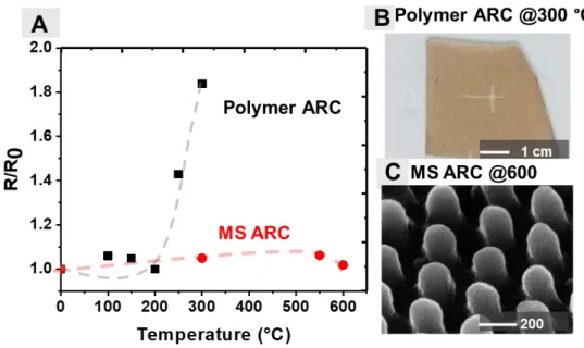
Thermal resistance
An assessment of the resilience of our structures against heating has been conducted to evaluate their thermal resistance (see Figure 4). We followed a protocol similar to that previously employed for the mechanical abrasion.
The reflectivity evolution has been monitored from room temperature up to 600 °C in steps of 50 °C (15 min annealing per step) in air. The increase in reflectivity is evident for the polymer after 300 °C, as a result of its thermal decomposition (also confirmed by optical inspection of the master polymer that becomes darker after annealing). However, the methylated silica replica features only a slight change of the reflectance ratio in all the investigated temperature range confirming its high thermal stability. SEM images after annealing account for this stability by revealing the unchanged features at the surface of the sample after 600 °C. This test demonstrates the remarkable robustness of silica-based ARCs and opens the possibility to use it for high optical transmission windows exposed to extreme conditions.
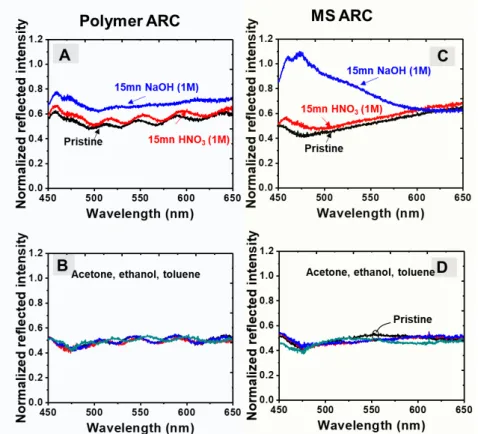
Chemical resistance
Once more, the same optical detection protocol was used to assess the stability of the ARCs when exposed to different, extreme, chemical conditions (pH, solvent). The test consists of
Figure 4. A) Reflection intensity, measured for both polymer ARC and MS ARC (methylated silica), under
an optical microscope, as described in Figure 3 D (same conditions), with respect to temperature. The values of the reflected intensity have been averaged in the measured spectral range and normalized to the initial value at room temperature, (R0). B) Optical image of polymer ARC after 15 min at 300°C. C)
dipping the samples for 15 minutes in acetone, ethanol, toluene, and acidic/oxidizing (aqueous 1M HNO3) or alkaline (aqueous 1M NaOH) solutions. The reflected intensity after dipping is normalized to that of the initial value before chemical attack (Figure 5). Both polymer and silica-based ARCs are stable in polar and non-polar solvents, since no modification of the reflectivity has been observed. Concerning pH sensitivity, both systems are also extremely stable in acidic and oxidizing conditions. However, 15 min in 1Mol sodium hydroxide induces an irreversible decrease of the reflectivity, suggesting that they have been chemically modified by the hydroxyl ions present in the solution. We attribute this change to the instability of silica at pH > 10. 37 In
our case, it shows an improved stability, comparable to the polymer one, as a result of its combination with methyl groups that makes it water repellent and therefore more stable in water.
38 The difference in the spectral features of the reflectivity between both polymer and inorganic
ARC is likely due to the difference in chemical attack mechanism that induce a different evolution of the refractive index profile. The study of the chemical mechanism behind this deterioration is out of the scope of the present work and has not been instigated.
Discussion
Figure 5. Reflection spectra both polymer ARC and MS ARC (Methylated Silica) before (pristine) and after immersion for 15 min in 1M nitric acid (HNO3), 1M sodium hydroxide (NaOH), (A and C respectively ), and acetone, ethanol and toluene (B and D, respectively)
In the light of the previous considerations, direct printing of a sol-gel solution is a competitive and promising use of NIL processing for ARC. In fact, it enables the formation of high 39,15 and
low dielectric constant materials 28and it skips many of the more or less cumbersome steps
required by top-down etching.
Finally, NIL has been extensively exploited for etching low dimensional structures. Its direct use with polymers has been one of the first examples to produce efficient ARC. 1, 40 However, owing
to the limited dielectric constant of this class of materials, they can be used as ARC only on comparably low refractive index substrates (e.g. glass). In addition to this, as we thoroughly demonstrated in our work, they suffer from a relatively low resistance to rubbing and to high temperature, rendering them less adapted to work in extreme conditions with respect to more stable, dielectric materials as the silica used here.
A further use of NIL of polymers for ARC includes further etching steps: first a polymeric resist is spread on a surface, printed with a mold and densified (e.g. by heating or UV curing). These printed structures are used to protect the parts of underlying surface that should be preserved during the following etching step that can be performed via selective chemical attack or via reactive ion etching. Finally, the residual resist is removed with a solvent leaving 3D structures (that can be eventually of larger refractive index of the polymer used for the NIL step). This is for instance the process used some study 39 to create a broad-band and broad-angle ARC on a Si
wafer. Due to the many steps required in this approach, this kind of ARC, although performing, is hardly scalable (e.g. to a roll-to-roll chain of production).
Conclusion
To summarize, we showed that sol-gel soft-NIL method can be implemented on at least 10 cm diameter substrates, which is extremely well-adapted to elaborate graded ARCs (mostly single or double faces) on glass. The total transmission reaches 96~97% in the whole visible range (limited by the scattering from the underlying glass substrate), and for angular incidences below 60 degrees, with less than 1% fluctuation in the investigated spectral range. We also demonstrate that the sol-gel materials combined with a nipple-dimple conformation gathers optimal optical performances high stability, against abrasion, extreme temperatures, and chemical attacks. These results confirm that, due to their processability, the versatility to adjust their optical constants, and their robustness, sol-gel materials are ideal systems to serve as nanostructured ARC over large surfaces.
Experimental sections
Preparation of Methylated Silica (Si4O7Me2) sol gel solution. Methylated silica (Si4O7Me2)
sol-gel solution was prepared by mixing 0.5 TEOS, 0.5 MTEOS, 20 EtOH (Absolute), 5 H2O
(deionized) and 4.10-4 Pluronic F127 (PEO-b-PBO), molar ratios. After 24h aging, the solution
was spin coated on glass at 1500 rpm (10s) in room conditions (POLOS TM). All chemicals were purchased from Aldrich.
NIL procedure via preparation of the nano patterned ARC morphologies. As-prepared
coatings were then transferred into a nano-imprint chamber in which a 70% relative humidity was maintained using a constant 5L.min-1 flux of air generated from a home-made humidity controller
system. The nano-imprint was performed less than 1 min after spin-coating by applying the PDMS mold onto the sol-gel film. Before unmolding, the system was cured at 60 °C for 10 min. The imprinted samples were then annealed at 450°C for 20 min to ensure the complete removal of the F127 polymer and the condensation of the silica backbone. The PDMS mold was replicated from a commercial Perfluoropolyether Fluorolink (MD700) master. The master surface was rendered hydrophobic by immersion for 10 min in a solution of 0.05M SiCl2 (Me)2 in
ethanol, followed by an abundant rinsing with ethanol. The PDMS precursors and reactant mixture (90w% RTV141A ; 10w% RTV141B from BLUESIL) was then poured onto the functionalized master surface and cured at 70°C for one night. The PDMS replica (mold) is then peeled off the master surface after cooling. The mold is pumped in primary vacuum for 10 min before imprinting as described previously 15.
Optical measurement and characterization of NIL based ARC. The refractive index and the
thickness of methylated silica (Si4O7Me2) sol-gel coating were measured on flat (not imprinted)
zones of the sample, using spectroscopic Ellipsometry (Woollan M2000V) and fitting the ellipsometry data with standard Cauchy model. Structural investigation of the nano-imprinted samples was performed by Atomic Force Microscopy (AFM) (PSIA XE-100 AFM) and high-resolution scanning electron microscopy FEI Strata DB235 (with 5 kV electron acceleration voltage). Abrasion resistance were performed using a crock meter test, that consists in rubbing off, with a back and forth motion, the top of the films with a pad covered with a calibrated fabric (ISO test method 105-F09) and loaded with a constant charge of 5 N (Pressure = 2.08 Ncm-2).
Optical characterization has been performed with a spectrophotometer (Perkin Elmer) mounting an integrating sphere (quasi-normal incidence for total reflection, total transmission and reflected diffusion). Angular dependence of specular reflection (θillumination = θdetection) is measured with a
goniometer by scanning the incidence angle of the light beam from 5 to 70 degrees. The reflected light is collected within a multimode optical fiber (50 μm, Figure 3D). The evolution of the normalizedm core diameter) and fed into a spectrometer (from Ocean Optics). Optical characterization of the reflected intensity after crock meter, annealing and chemical attacks was performed using a commercial ZEISS optical microscope (objective lens with magnification 10X, numerical aperture NA = 0.25). A confocal optical fiber (50 μm, Figure 3D). The evolution of the normalizedm core diameter) is coupled with a spectrometer determining a lateral resolution of ~50 μm, Figure 3D). The evolution of the normalizedm.
Thermal stability test on ARC Films. ARC based on Methylated silica and polymer were
tested against annealing in air. Temperature ranged between 100 and 600 °C and was changed in intervals of 50 °C. All the samples were exposed for 15 minutes for each temperature step.
Chemical stability test on ARC films. ARC based on Methylated silica and polymer were tested
against chemical attacks to test their stability. The test consisted in dipping the samples for 15 minutes in acetone, ethanol, toluene, and acidic/oxidizing (aqueous 1M HNO3) or alkaline
Acknowledgment and funding
This material is based on work supported in part by the National Science Foundation under the Interna-tional Research Fellowship Program, Grant OISE-0505786. The authors also acknowledge funding provided by CNRS and UPMC, the PRCI network ULYSSES (No. ANR-15-CE24-0027-01) funded by the French ANR agency, the A∗MIDEX foundation (ANR-11-IDEX-0001-02), the A∗MIDEX Project TITANIDE (No. A-M-AAP-EI-17-58-170228-16.21-ABBARCHI-SAT), the FET-OPEN project NARCISO (No. 828890). We acknowledge the facilities of the NANOTECMAT platform at the IM2NP Institute.
Author information
Corresponding author
David Grosso Professor Université Aix Marseille, Chaire of Excellence AMIDEX,IM2NP
-UMR CNRS 7334, Aix-Marseille Université, Faculté des Sciences de Saint Jérôme, Case 142, 13397 Marseille Cedex 20, France.
ORCID : https://orcid.org/0000-0002-9156-6848
Email : [email protected]
Marco Abbarchi- Maître de conférences NSE, IM2NP (CNRS), University Aix-Marseille 3,
Campus St Jérôme, 13397
ORCID : https://orcid.org/0000-0002-2760-4766
Email : [email protected] Authors
Mehrnaz Modaresialam – PhD researcher IM2NP (CNRS), University Aix-Marseille 3,
Campus St Jérôme, 13397
ORCID: https:// orcid .org/0000-0001-8568-8323
Jean Benoit Claud – Post doc researcher IM2NP (CNRS), University Aix-Marseille 3, Campus
St Jérôme, 13397
ORCID:https://orcid.org/ 0000-0001-9618-0576
Abbreviations
ARC Anti Reflection Coating; NIL Nano Imprint Lithography; MS Methylated Silica; PDMS Polydimethylsiloxane; PFPE Perfluoropolyether; BRDF Bidirectional Reflectance Distribution Function; SEM Scanning Electron Microscopy; AFM Atomic Force Microscop; DF MS ARC Double face Methylated Silica
References
(1) Raut, H. K.; Ganesh, V. A.; Nair, A. S.; Ramakrishna, S. Anti-Reflective Coatings: A Critical, in-Depth Review. Energy Environ. Sci. 2011, 4 (10), 3779.
https://doi.org/10.1039/c1ee01297e.
(2) Ootsuka, T.; Liu, Z.; Osamura, M.; Fukuzawa, Y.; Kuroda, R.; Suzuki, Y.;
Otogawa, N.; Mise, T.; Wang, S.; Hoshino, Y.; Nakayama, Y.; Tanoue, H.; Makita, Y. Studies on Aluminum-Doped ZnO Films for Transparent Electrode and
Antireflection Coating of β-FeSi2 Optoelectronic Devices. Thin Solid Films 2005, 476 (1), 30–34. https://doi.org/10.1016/j.tsf.2004.06.145.
(3) Raut, H. K.; Dinachali, S. S.; Loke, Y. C.; Ganesan, R.; Ansah-Antwi, K. K.; Góra, A.; Khoo, E. H.; Ganesh, V. A.; Saifullah, M. S. M.; Ramakrishna, S. Multiscale Ommatidial Arrays with Broadband and Omnidirectional Antireflection and Antifogging Properties by Sacrificial Layer Mediated Nanoimprinting. ACS Nano 2015, 9 (2), 1305–1314. https://doi.org/10.1021/nn5051272.
(4) Han, K.-S.; Shin, J.-H.; Yoon, W.-Y.; Lee, H. Enhanced Performance of Solar Cells with Anti-Reflection Layer Fabricated by Nano-Imprint Lithography. Sol. Energy Mater. Sol. Cells 2011, 95 (1), 288–291.
https://doi.org/10.1016/j.solmat.2010.04.064.
(5) Elshorbagy, M. H.; Abdel-Hady, K.; Kamal, H.; Alda, J. Broadband Anti-Reflection Coating Using Dielectric Si3N4 Nanostructures. Application to Amorphous-Si-H Solar Cells. Opt. Commun. 2017, 390, 130–136.
https://doi.org/10.1016/j.optcom.2016.12.062.
(6) Ye, L.; Zhang, Y.; Zhang, X.; Hu, T.; Ji, R.; Ding, B.; Jiang, B. Sol–Gel Preparation of SiO2/TiO2/SiO2–TiO2 Broadband Antireflective Coating for Solar Cell Cover Glass. Sol. Energy Mater. Sol. Cells 2013, 111, 160–164.
https://doi.org/10.1016/j.solmat.2012.12.037.
(7) Yanagishita, T.; Kondo, T.; Masuda, H. Preparation of Renewable Antireflection Moth-Eye Surfaces by Nanoimprinting Using Anodic Porous Alumina Molds. J. Vac. Sci. Technol. B Nanotechnol. Microelectron. Mater. Process. Meas. Phenom. 2018, 36 (3), 031802. https://doi.org/10.1116/1.5016369.
(8) Wei, W.; Zhu, X.; Zhao, Y.; Wu, Q. Nanometer SiO2 Antireflection Coating for Solar Modules. 2015, 4.
(9) Ting, C.-J.; Huang, M.-C.; Tsai, H.-Y.; Chou, C.-P.; Fu, C.-C. Low Cost Fabrication of the Large-Area Anti-Reflection Films from Polymer by
Nanoimprint/Hot-Embossing Technology. Nanotechnology 2008, 19 (20), 205301. https://doi.org/ 10.1088/0957-4484/19/20/205301.
(10) Boudot, M.; Gaud, V.; Louarn, M.; Selmane, M.; Grosso, D. Sol–Gel Based Hydrophobic Antireflective Coatings on Organic Substrates: A Detailed
Investigation of Ammonia Vapor Treatment (AVT). Chem. Mater. 2014, 26 (5), 1822–1833. https://doi.org/10.1021/cm403787v.
(11) Spinelli, P.; Verschuuren, M. A.; Polman, A. Broadband Omnidirectional Antireflection Coating Based on Subwavelength Surface Mie Resonators. Nat. Commun. 2012, 3 (1), 692. https://doi.org/10.1038/ncomms1691.
(12) Cordaro, A.; van de Groep, J.; Raza, S.; Pecora, E. F.; Priolo, F.; Brongersma, M. L. Antireflection High-Index Metasurfaces Combining Mie and Fabry-Pérot
Resonances. ACS Photonics 2019, 6 (2), 453–459. https://doi.org/10.1021/acsphotonics.8b01406.
(13) Bouabdellaoui, M.; Checcucci, S.; Wood, T.; Naffouti, M.; Sena, R. P.; Liu, K.; Ruiz, C. M.; Duche, D.; le Rouzo, J.; Escoubas, L.; Berginc, G.; Bonod, N.; Zazoui, M.; Favre, L.; Metayer, L.; Ronda, A.; Berbezier, I.; Grosso, D.; Gurioli, M.;
Abbarchi, M. Self-Assembled Antireflection Coatings for Light Trapping Based on SiGe Random Metasurfaces. Phys. Rev. Mater. 2018, 2 (3).
https://doi.org/10.1103/PhysRevMaterials.2.035203.
(14) Lin, A.; Zhong, Y.-K.; Fu, S.-M. The Versatile Designs and Optimizations for Cylindrical TiO_2-Based Scatterers for Solar Cell Anti-Reflection Coatings. Opt. Express 2013, 21 (S6), A1052. https://doi.org/10.1364/OE.21.0A1052.
(15) Bottein, T.; Wood, T.; David, T.; Claude, J. B.; Favre, L.; Berbézier, I.; Ronda, A.; Abbarchi, M.; Grosso, D. “Black” Titania Coatings Composed of Sol-Gel Imprinted Mie Resonators Arrays. Adv. Funct. Mater. 2017, 27 (2), 1604924. https://doi.org/10.1002/adfm.201604924.
(16) Keshavarz Hedayati, M.; Abdelaziz, M.; Etrich, C.; Homaeigohar, S.; Rockstuhl, C.; Elbahri, M. Broadband Anti-Reflective Coating Based on Plasmonic
Nanocomposite. Materials 2016, 9 (8), 636. https://doi.org/10.3390/ma9080636.
(17) Hiller, J.; Mendelsohn, J. D.; Rubner, M. F. Reversibly Erasable Nanoporous Anti-Reflection Coatings from Polyelectrolyte Multilayers. Nat. Mater. 2002, 1 (1), 59–63. https://doi.org/10.1038/nmat719.
(18) Buskens, P.; Burghoorn, M.; Mourad, M. C. D.; Vroon, Z. Antireflective Coatings for Glass and Transparent Polymers. Langmuir 2016, 32 (27), 6781–6793. https://doi.org/10.1021/acs.langmuir.6b00428.
(19) He, J.; Ke, Y. Plasma-Enhanced Chemical Vapor-Deposited SiN and Liquid-Phase-Deposited SiO2 Stack Double-Layer Anti-Reflection Films for Multi-Crystalline Solar Cells. Superlattices Microstruct. 2018, 122, 296–303. https://doi.org/10.1016/j.spmi.2018.07.035.
(20) Bläsi, B.; Tucher, N.; Höhn, O.; Kübler, V.; Kroyer, T.; Wellens, Ch.; Hauser, H. Large Area Patterning Using Interference and Nanoimprint Lithography;
Thienpont, H., Mohr, J., Zappe, H., Nakajima, H., Eds.; Brussels, Belgium, 2016; p 98880H. https://doi.org/10.1117/12.2228458.
(21) Burghoorn, M.; Roosen-Melsen, D.; de Riet, J.; Sabik, S.; Vroon, Z.; Yakimets, I.; Buskens, P. Single Layer Broadband Anti-Reflective Coatings for Plastic
Substrates Produced by Full Wafer and Roll-to-Roll Step-and-Flash Nano-Imprint Lithography. Materials 2013, 6 (9), 3710–3726.
https://doi.org/10.3390/ma6093710.
(22) Shin, J.-H.; Go, B.-N.; Choi, H.-J.; Cho, J.-Y.; Lee, A. S. S.; Hwang, S. S.; Cha, H. J.; Lee, H. Fabrication of Functional Nanosized Patterns with UV-Curable
Polysilsesquioxane on Photovoltaic Protective Glass Substrates Using Hybrid Nano-Imprint Lithography. J. Mater. Chem. C 2014, 2 (29), 5864–5869. https://doi.org/10.1039/C4TC00101J.
(23) Fabrication of n‐ and p‐Type Organic Thin Film Transistors with Minimized Gate Overlaps by Self‐Aligned Nanoimprinting https://onlinelibrary-wiley-com.lama.univ-amu.fr/doi/epdf/10.1002/adma.201001947 (accessed Apr 29, 2020).
(24) Zou, Y.; Moreel, L.; Lin, H.; Zhou, J.; Li, L.; Danto, S.; Musgraves, J. D.; Koontz, E.; Richardson, K.; Dobson, K. D.; Birkmire, R.; Hu, J. Solution Processing and Resist-Free Nanoimprint Fabrication of Thin Film Chalcogenide Glass Devices:
Inorganic–Organic Hybrid Photonic Integration. Adv. Opt. Mater. 2014, 2 (8), 759–764. https://doi.org/10.1002/adom.201400068.
(25) Dinachali, S. S.; Dumond, J.; Saifullah, M. S. M.; Ansah-Antwi, K. K.; Ganesan, R.; Thian, E. S.; He, C. Large Area, Facile Oxide Nanofabrication via Step-and-Flash Imprint Lithography of Metal–Organic Hybrid Resins. ACS Appl. Mater. Interfaces 2013, 5 (24), 13113–13123. https://doi.org/10.1021/am404136p. (26) Park, H.-H.; Choi, D.-G.; Zhang, X.; Jeon, S.; Park, S.-J.; Lee, S.-W.; Kim, S.; Kim,
K.; Choi, J.-H.; Lee, J.; Yun, D. K.; Lee, K. J.; Park, H.-H.; Hill, R. H.; Jeong, J.-H. Photo-Induced Hybrid Nanopatterning of Titanium Dioxide via Direct Imprint Lithography. J. Mater. Chem. 2010, 20 (10), 1921.
https://doi.org/10.1039/b921343k.
(27) Bottein, T.; Dalstein, O.; Putero, M.; Cattoni, A.; Faustini, M.; Abbarchi, M.; Grosso, D. Environment-Controlled Sol–Gel Soft-NIL Processing for Optimized Titania, Alumina, Silica and Yttria-Zirconia Imprinting at Sub-Micron Dimensions. Nanoscale 2018, 10 (3), 1420–1431. https://doi.org/10.1039/C7NR07491C. (28) van de Groep, J.; Spinelli, P.; Polman, A. Single-Step Soft-Imprinted Large-Area
Nanopatterned Antireflection Coating. Nano Lett. 2015, 15 (6), 4223–4228. https://doi.org/10.1021/acs.nanolett.5b01623.
(29) Nanoimprint Lithography on Silica Sol–Gels: A Simple Route to Sequential Patterning https://onlinelibrary-wiley-com.lama.univ-amu.fr/doi/epdf/10.1002/ adma.200702484 (accessed Apr 29, 2020).
(30) Deniz, H.; Khudiyev, T.; Buyukserin, F.; Bayindir, M. Room Temperature Large-Area Nanoimprinting for Broadband Biomimetic Antireflection Surfaces. Appl. Phys. Lett. 2011, 99 (18), 183107. https://doi.org/10.1063/1.3657766.
(31) Hong, S.-H.; Bae, B.-J.; Han, K.-S.; Hong, E.-J.; Lee, H.; Choi, K.-W. Imprinted Moth-Eye Antireflection Patterns on Glass Substrate. Electron. Mater. Lett. 2009, 5 (1), 39–42. https://doi.org/10.3365/eml.2009.03.039.
(32) Navarro-Baena, I.; Jacobo-Martín, A.; Hernández, J. J.; Castro Smirnov, J. R.; Viela, F.; Monclús, M. A.; Osorio, M. R.; Molina-Aldareguia, J. M.; Rodríguez, I. Single-Imprint Moth-Eye Anti-Reflective and Self-Cleaning Film with Enhanced Resistance. Nanoscale 2018, 10 (33), 15496–15504.
https://doi.org/10.1039/C8NR02386G.
(33) Berman, D.; Guha, S.; Lee, B.; Elam, J. W.; Darling, S. B.; Shevchenko, E. V. Sequential Infiltration Synthesis for the Design of Low Refractive Index Surface Coatings with Controllable Thickness. ACS Nano 2017, 11 (3), 2521–2530. https://doi.org/10.1021/acsnano.6b08361.
(34) Yoo, Y. J.; Kim, Y. J.; Kim, S.-Y.; Lee, J. H.; Kim, K.; Ko, J. H.; Lee, J. W.; Lee, B. H.; Song, Y. M. Mechanically Robust Antireflective Moth-Eye Structures with a Tailored Coating of Dielectric Materials. Opt. Mater. Express 2019, 9 (11), 4178. https://doi.org/10.1364/OME.9.004178.
(35) Womack, G.; Isbilir, K.; Lisco, F.; Durand, G.; Taylor, A.; Walls, J. M. The Performance and Durability of Single-Layer Sol-Gel Anti-Reflection Coatings Applied to Solar Module Cover Glass. Surf. Coat. Technol. 2019, 358, 76–83. https://doi.org/10.1016/j.surfcoat.2018.11.030.
(36) Khan, S. B.; Wu, H.; Xie, Z.; Wang, W.; Zhang, Z. Al 2 O 3 Encapsulated Teflon Nanostructures with High Thermal Stability and Efficient Antireflective
Performance. ACS Appl. Mater. Interfaces 2017, 9 (41), 36327–36337. https://doi.org/10.1021/acsami.7b12903.
(37) Brinker, C. J. Dip Coating. In Chemical Solution Deposition of Functional Oxide Thin Films; Schneller, T., Waser, R., Kosec, M., Payne, D., Eds.; Springer Vienna: Vienna, 2013; pp 233–261. https://doi.org/10.1007/978-3-211-99311-8_10. (38) Loizillon, J.; Putero, M.; Grosso, D. Tuning Mesoporous Silica Film Accessibility
Through Controlled Dissolution in NH 4 F: Investigation of Structural Change by Ellipsometry Porosimetry and X-Ray Reflectivity. J. Phys. Chem. C 2019, 123 (50), 30398–30406. https://doi.org/10.1021/acs.jpcc.9b09109.
(39) Spinelli, P.; Macco, B.; Verschuuren, M. A.; Kessels, W. M. M.; Polman, A. Al 2 O 3 /TiO 2 Nano-Pattern Antireflection Coating with Ultralow Surface
Recombination. Appl. Phys. Lett. 2013, 102 (23), 233902. https://doi.org/10.1063/1.4810970.
(40) Tatsi, E.; Griffini, G. Polymeric Materials for Photon Management in Photovoltaics. Sol. Energy Mater. Sol. Cells 2019, 196, 43–56.