HAL Id: tel-03222154
https://tel.archives-ouvertes.fr/tel-03222154
Submitted on 10 May 2021HAL is a multi-disciplinary open access archive for the deposit and dissemination of sci-entific research documents, whether they are pub-lished or not. The documents may come from teaching and research institutions in France or abroad, or from public or private research centers.
L’archive ouverte pluridisciplinaire HAL, est destinée au dépôt et à la diffusion de documents scientifiques de niveau recherche, publiés ou non, émanant des établissements d’enseignement et de recherche français ou étrangers, des laboratoires publics ou privés.
FDSOI and beyond
Mohammed Tmimi
To cite this version:
Mohammed Tmimi. Novel approach for serial data link in 28nm CMOS FDSOI and beyond. Micro and nanotechnologies/Microelectronics. Université Grenoble Alpes [2020-..], 2020. English. �NNT : 2020GRALT079�. �tel-03222154�
DOCTEUR DE L’UNIVERSITE GRENOBLE ALPES
Spécialité : Nano Electronique et Nano TechnologiesArrêté ministériel : 25 mai 2016
Présentée par
Mohammed TMIMI
Thèse dirigée par Philippe GALY, et
codirigée par Philippe FERRARI, Stefano D’AMICO, Jean-Marc DUCHAMP
préparée au sein du Laboratoire RFIC
dans l'École Doctorale Electronique, Electrotechnique, Automatique et Traitement du Signal (EEATS)
Nouvelle approche pour lien série
en technologie FD-SOI 28 nm
CMOS avancée et au-delà
Thèse soutenue publiquement le 16 décembre 2020, devant le jury composé de :Monsieur Jean-Baptiste BEGUERET
Professeur, Université de Bordeaux, Rapporteur
Monsieur Andrea MAZZANTI
Professeur, Univérsité de Pavia, Rapporteur
Madame Anne-Laure BILLABERT
Maitre de conférences HDR, Le Cnam/ESYCOM Paris, Examinatrice
Monsieur Sylvain BOURDEL
Professeur, Univérsité de Grenoble Alpes, Président
Monsieur Philippe GALY
Directeur technique, HDR, STMicroelectronics, Directeur de thèse
Monsieur Philippe FERRARI
Professeur, Univérsité de Grenoble Alpes, Co-directeur de thèse, invité
Monsieur Stefano D’AMICO
Maitre de conférences, Univérsité de salento, Co-encadrant de thèse, invité
Monsieur Jean-Marc DUCHAMP
Maitre de conférences, Univérsité de Grenoble Alpes, Co-encadrant de thèse, invité
Monsieur Philippe CATHELIN
“Real knowledge is to know the extent of one's ignorance.”
- Confucius
Abstract
The global internet traffic exceeded the zettabyte marker in 2016, initiating the zettabyte traffic era. Since then, internet traffic proliferated with a compound annual growth rate of 26%; and is expected to continue its astronomical growth rate. This perpetual growth has significant implications for networking technologies and their present limits. Researchers anticipated these limits and managed to stay ahead of the curve by innovating and optimizing all data transfer levels. In that context, this work focuses on on-chip data transfer, acknowledging that communication energy efficiency is one of the integrated circuits near future bottlenecks, as the gap between the computation energy and on-die IC energy grows.
Evidently, improvements have to be made to the existing links solutions; higher data rates must be reached while considering the energy efficiency and the circuit complexity. Furthermore, with the increasing data rates, signal integrity problems arise due to channel imperfections. Although transistor scaling provided higher density packing of devices along with faster transistors, it did not benefit the interconnections performance since it resulted in higher wires density. Wires are more sensitive to their environment than active devices, that is, closer wires are more sensible to crosstalk and longer delay due to the wire's intrinsic delay. Delay is a critical metric for data transmission, and lower controlled delay is favored. In this work, we developed a high data-rate low delay solution for long-range on-chip serial links. The developed solution is complementary to the massively employed existing solutions. We believe it will help solve some of their issues and extend the existing Network on chips (NoC) architectures lifetime.
We start this work by introducing the standard and emerging on-chip interconnect solutions, then discussing their advantages and challenges. Clearly, each solution is suitable for specific applications. The chosen RF interconnects technique is most suitable for our requirements, mainly due to low delay, high available bandwidths, and CMOS process compatibility/friendliness. This approach requires transmitting the data at high frequencies instead of the baseband, that is, up-converting the data signal before transmitting it through the transmission lines. In practice, transmission lines behave differently at baseband and high-frequencies. In particular, both distortion and delay are much lower at high-frequencies. These two properties are essential for our work; low distortion implies that high signal integrity is reached without equalization or error-correcting codes, up to 14 Gbps in the proposed study. At least four times lower than baseband delay, the high-frequency low delay property signifies that long distances across the chip can be crossed in less time.
We believe this approach is most beneficial for distances longer than a couple of millimeters and up to twentieth millimeters.
Bandwidth at higher frequencies (60 GHz in our case) is a valuable commodity. To take full advantage of the available bandwidth, we choose to use duobinary modulation to double the data rate within the same bandwidth. This spectrum compression relaxes the RF components constraints such as linearity; The chosen modulation also allows for simple demodulation where a simple envelope detector is used to recover the 14 Gbps data.
A 10 Gbps prototype chip was designed and fabricated in the advanced 28 nm FD-SOI technology from STMicroelectronics. This technology is introduced in the third chapter; afterward, we explained the design process of the 10 Gbps transceiver (composed of a transmitter, a receiver, and a 4.6mm channel). The simulation results showed that we reached a higher data rate (at least double) than the state of the art, for a smaller area and a comparable energy efficiency. The post-layout simulation resulted in a BER lower than 10−12. The measurement results will be published in future works.
We also proposed to use the same approach for interposer channels to connect chiplets with minimal delay. We study its application for a 130 nm BiCMOS technology passive silicon interposer, but it can be used for active ones too. We connected two 28 nm FD-SOI chiplets at a 7-mm distance and achieved a BER lower than 10−12 with a 7 ps/mm delay in simulations.
Résumé
Dans le cadre de l’échange massif de données numériques, la solution du lien série est largement utilisée dans les systèmes électroniques. Dans ce cadre, il existe une course permanente pour accroître le débit de transfert de données. Notamment les efforts portent sur l’amélioration de l’efficacité énergétique du système et l’optimisation des canaux de transmission. Cependant la contrainte physique du canal de transmission est une donnée majeure dans cette approche de transmission de données à haut débit.
Les méthodes standard de transmission intra-puces point à point utilisent la bande de base, le délai de transmission dans cette bande se situe autour de 40 ps/mm, acceptable pour des distances courtes inférieures au mm. Or, pour un lien de quelques mm, la solution standard d’utiliser des routeurs n’est plus optimale quant à la consommation et au temps de transfert dus à la propagation du signal en bande de base. En conséquence, un changement de paradigme est nécessaire afin de réduire ce délai.
Aujourd’hui, les recherches sont très actives concernant l’intégration monolithique de lien série, ce qui permet d’avoir une excellente base de concepts et de solutions. Dans la littérature, on note ainsi plusieurs solutions, la principale étant la transmission sans-fil puces « wireless on-chip (WiNOC) », où des antennes intra-puces sont utilisées pour transmettre les données. On peut également noter l’utilisation de l’optoélectronique pour transmettre avec un délai minimal. Il en résulte un changement de processus.
Dans ce travail, on vise les liens de quelques mm de long, où aucune des solutions précédentes n’est optimale, soit à cause du temps de propagation soit à cause de la complexité de l’implémentation due au changement du procédé. Cette solution est complémentaire aux solutions existantes et nous pensons qu’elle permet de résoudre certains de leurs problèmes et prolonger la durée de vie des architectures réseau sur puces (NoC) existantes.
On investigue la transmission en bande millimétrique (à 60 GHz) où la vitesse de propagation du signal est autour de 1,5. 108 m/s, impliquant un délai minimal (7 ps/mm). Par ailleurs, différentes modulations seront investiguées pour augmenter le débit et exploiter efficacement les bandes passantes disponibles à ces fréquences. On a choisi la modulation duobinaire pour son avantage en termes de compression du spectre, ce qui nous a permis de doubler le débit utilisé pour une même bande passante, ainsi que pour sa simplicité de modulation/démodulation. Dans notre cas, on utilise 5 GHz de bande pour transmettre un signal de 10 Gbps.
Cette approche théorique a été modélisée pour ensuite la comparer aux différents systèmes à l’état de l’art ; un débit maximal de 14 Gbps a été atteint avec un taux d’erreur inférieur a 10−12 en simulation. Un démonstrateur sur silicium à 10 Gbps a été conçu sur la base de la technologie CMOS avancée 28 nm FD-SOI de STMicroelectronics. Le transmetteur, le récepteur ainsi que des lignes de propagation d’une longueur de 4.6 mm ont été implémentés, les résultats de mesures seront publiées dans de futurs travaux. Les simulations ont montré que nous avons atteint un
débit plus élevé (au moins le double) que l’état de l’art, pour une surface plus faible et une efficacité énergétique comparable.
Nous avons également proposé d'utiliser la même approche pour les canaux d’interposeurs afin de connecter des chiplets avec un délai minimal. Nous étudions son application pour un interposeur passif en silicium en technologie BiCMOS 130 nm, mais il peut également être utilisé pour les circuits actifs. Nous avons connecté deux puces en technologie 28 nm FD-SOI à une distance de 7 mm et obtenu un taux d’erreur binaire inférieur à 10−12avec une latence de 7 ps / mm en simulation.
Acknowledgment
It is a pleasure to thank the many people that made this thesis possible.
Firstly, I would like to express my sincere gratitude to my advisors Philippe Galy, Philippe Ferrari, Jean-Marc Duchamp, and Stefano D'Amico for the continuous support of my Ph.D. research and their patience. Their guidance helped me in all the time of research and writing of this thesis. I am incredibly grateful for their confidence and the freedom they gave me to do this work.
I would like to thank my thesis committee members for their time, their invaluable feedback and intellectual contributions.
My special appreciation and thanks go to Philippe Cathelin, a great mentor, for his guidance and support.
I would also like to acknowledge with gratitude Andreia Cathelin, Stéphane Le Tual, Sylvain Clerc, Denis Pache, and Roberto Guizzetti for their help and insightful comments. I am also extending my thanks to the bat.6000 colleagues and friends: Olivier Jeantet, Raphael Gras, Tarun Chawla, Thomas Ahrens, Bruno Spy, Sebastien Peurichard, and Daniel Pierredon.
I am grateful to my friends and Ph.D. students from STMicroelectronics Crolles with whom I shared enjoyable moments. Thanks to Valérian Cinçon, Ioanna Kriekouki, Geoffrey Delahaye, David Gaidioz, Zoltan Nemes, Clément Beauquier, Antoine Le Ravallec, Guillaume Tochou, Alexis Rodrigo Iga Jadue, Romane Dumont, Robin Benarrouch, Angel De Dios Gonzales Santos, Thibault Despoisse, Sebastien Sadlo, Dayana Andrea Pino Monroy and Soufiane Mourrane.
Special thanks to Thomas Bédécarrats, Renan Lethiecq, Louise De Conti, Raphael Guillaume, Florian Voineau, Abdelhakim Mahjoub, Yassine Oussaïti and Ioana Andrada Burducea for the support and kindness, words cannot express how grateful I am.
Most importantly, none of this could have happened without my family. To my parents, I am extremely grateful for your encouragement, caring, and sacrifices. To my sisters, Narimane and Meryame, thank you for your support and encouragement. I will be grateful forever for your love.
Table of Contents
CONTEXT ... 1
MOTIVATION ... 2
THESIS OUTLINE ... 4
I.AN INTRODUCTION INTO EMERGING ON-CHIP INTERCONNECTS ... 6
II.HIGH SPEED SERIAL LINK ARCHITECTURE ... 9
II.1. Line coding ... 10
II.2. Bandpass modulation ... 11
III.SERIAL LINK PERFORMANCE METRICS ... 11
III.1. Eye Diagram ... 11
III.2. Bit error rate ... 12
III.3. Error Vector Magnitude ... 13
III.4. Inter-symbol interference ... 14
III.5. Jitter ... 14
III.6. Error correcting codes ... 17
IV.ON-CHIP INTERCONNECTS ... 18
IV.1. RLCG model ... 18
IV.2. RC wire ... 23
IV.3. Transmission lines ... 34
V.RF-INTERCONNECT STATE OF THE ART ... 37
VI.CONCLUSION ... 42
VII.REFERENCES ... 43
I.OVERVIEW OF DATA TRANSMISSION MAIN FUNCTIONS ... 47
I.1. The bandwidth of a signal ... 47
I.2. Classical baseband modulations (NRZ, RZ, MLS) ... 48
I.3. Correlative baseband modulations ... 49
I.4. Intermediate frequency transposition ... 56
I.5. The channel: transmission lines ... 69
II.ARCHITECTURE SIMULATIONS ... 73
II.1. System architecture simulations results ... 73
II.2. Length adaptive serial link ... 76
II.3. Impact of some system components on the signal integrity ... 79
III.CONCLUSION ... 83
IV.REFERENCES ... 84
I.OVERVIEW OF THE 28NM FD-SOI TECHNOLOGY ... 87
I.1. The Back-end of line (BEOL) ... 88
II.THE CHANNEL ... 90
II.1. Electromagnetic simulations ... 90
II.2. The Microstrips ground plane ... 90
II.3. Edge-coupled microstrip lines ... 91
III.THE 10GBPS TRANSMITTER ARCHITECTURE ... 93
III.1. Clock buffers ... 94
III.2. Duobinary modulator ... 96
III.3. Mixer ... 97
III.4. Inputs matching ... 101
IV.THE 10GBPS RECEIVER ARCHITECTURE ... 102
IV.1. The matching network... 104
IV.2. The circuit's core ... 106
IV.3. 10Gbps transceiver simulation results ... 109
V.14GBPS SYSTEM SIMULATION RESULTS ... 112
VI.APPLICATION TO DIGITAL APPLICATIONS ... 113
VII.STATE OF THE ART COMPARISON ... 115
VIII.CONCLUSION ... 117
IX.REFERENCES ... 118
CONCLUSION ... 119
PERSPECTIVES ... 120
List of Figures
Figure 1 : Compute energy vs total on die IC energy for technology nodes. ... 1
Figure 2 : The proposed solution versus common interconnects distance range. ... 2
Figure 3: Possible usage applications of the proposed link. (a) Replace the long link in a NoC Torus topology with the proposed links.(b) Connect the furthest points directly. ... 3
Figure I.1 : Architecture of a typical NoC. ... 6
Figure I.2 : Architecture of a typical high-speed serail link. ... 9
Figure I.3 : Clock recovery and data retiming for a CDR circuit. ... 9
Figure I.4 : An example of unipolar signals ( RZ and NRZ). ... 10
Figure I.5 : An Eye diagram. ... 12
Figure I.6 : 𝐵𝐸𝑅 versus 𝐸𝑏/𝑁0 for different modulations. ... 13
Figure I.7 : (a) Ideal constellation diagram. (b) Measured constellation diagram. (c) Single error vector manitude calculation. ... 14
Figure I.8 : Inter-symbol interference. ... 14
Figure I.9 : Waveform timing variations. ... 15
Figure I.10 : Jitter components [17]. ... 15
Figure I.11 : Typical waveform including 𝑅𝐽, and 𝑅𝐽 Histogram[19]. ... 16
Figure I.12 : (a) Dual dirac method . (b) Typical 𝐷𝐽 Waveform, and histogram[19]. .. 16
Figure I.13 : a bathtub plot showing the BER as a function of sampling point delay. 17 Figure I.14: (a) An incremental length of a transmission line. (b) Lumped-element model. ... 18
Figure I.15 : Microstrip line and its electrical field lines. ... 20
Figure I.16 : Capacitive coupling between wires. ... 20
Figure I.17 : Skin effect flow primarily on the surface of the conductor. ... 21
Figure I.18 : Sketch of current distribution on a microstrip conductor [25]. ... 22
Figure I.19 : Mutual inductance between wires ... 23
Figure I.20 : Distributed and lumped model for a capacitance dominant wire ... 23
Figure I.21 : RC Distributed line. ... 24
Figure I.22 : (a) Crosstalk mechanisms. (b) timing uncertainty due to crosstalk. ... 26
Figure I.23 : shielding of sensitive signals. ... 27
Figure I.24 : (a) single-ended signaling. (b) Differential signaling. ... 28
Figure I.25 : Dispersion causes a pulse to spread out over time. ... 29
Figure I.26: Enhancing the high frequency components effect on the effective bandwidth [38]. ... 29
Figure I.27 : Passive implementation of a CTLE and its frequency response ... 30
Figure I.28 : Implementation of an active CTLE and its frequency response [42]. .... 31
Figure I.29 : A conventional FFE structure. ... 32
Figure I.30 : (a) Transmitted data with and without FFE equalization. (b) Received Data with and without FFE Equalization. ... 32
Figure I.31 : Comparison between CTLE and FFE spectrum, FFE amplifies odd harmonics of the Nyquist frequency [44]... 33
Figure I.32 : Conventional DFE architecture. ... 33
Figure I.33 : Structure of the main three types of the transmissions lines: (a) microstrip line (MSL), (b) differential line or coplanar strips (CPS), and (c) coplanar waveguide (CPW) [13]. ... 34
Figure I.34 : Group delay for a wire. ... 38
Figure I.35 : (a) Schematic of the tri-band RF-interconnect [53]. (b) On-chip differential TL [53]. ... 39
Figure I.36 : Architecture of the proposed system [54]. ... 40
Figure I.37 : 4-drop RF interconnect (Drop A multicasts) [56]. ... 41
Figure I.38 : On-chip directional coupler [56]. ... 41
Figure I.39 : Measured 𝐵𝐸𝑅 vs data rate at different drops [56]. ... 42
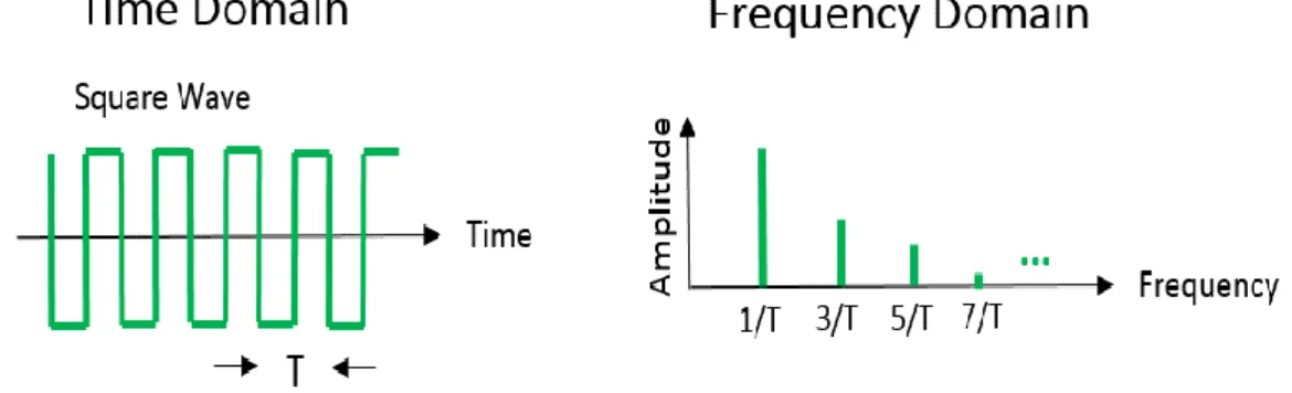
Figure II.1 : Time and frequency domain views of an ideal square wave. ... 47
Figure II.2 : Bandwidth of digital data. (a) Half-power. (b) Noise equivalent. (c) Null to null. (d) 99% of power. (e) Bounded PSD (defines attenuation outside bandwidth) at 35 and 50 dB [3]. ... 48
Figure II.3 : (a). Time-domain NRZ and PAM4 coding. (b). Comparison of an NRZ and PAM4 power spectrum [5]. ... 49
Figure II.4 :(a) NRZ eye diagram. (b) PAM4 eye diagram. ... 49
Figure II.5 : NRZ and duobinary: waveform, eye diagram, and spectrum [10]. ... 51
Figure II.6 : Spectrum and waveforms (data rate 20Gb/s) for different data formats passing through an ideal brickwall filter. (a) NRZ. (b) Duobinary [11]. ... 51
Figure II.7 : Eye diagram and Normalized power density spectrum: (a) PAM2. (b) PAM4. (c) Duobinary.[12]. ... 52
Figure II.8 : Duobinary precoder. (a) conventional. (b) Proposed [11]. ... 52
Figure II.9 : Original polybinary architecture [6]. ... 53
Figure II.10 : System architecture and duobinary required frequency response [13]. 54 Figure II.11 : Proposed implementation of the FIR pre-emphasis filter [14]. ... 54
Figure II.12 :(a) Proposed duobinary transmitter[11]. (b) Duobinary signaling model. ... 55
Figure II.13 : (a) Proposed duobinary-to-binary converter [14]. (b) Circuit truth table (c) Duobinary signal as an eye diagram and a time waveform. ... 55
Figure II.14 : Proposed duobinary-to-binary converter [11]... 56
Figure II.15 : Basic amplitude modulation [15]. ... 57
Figure II.16 : Basic amplitude demodulation[15]. ... 57
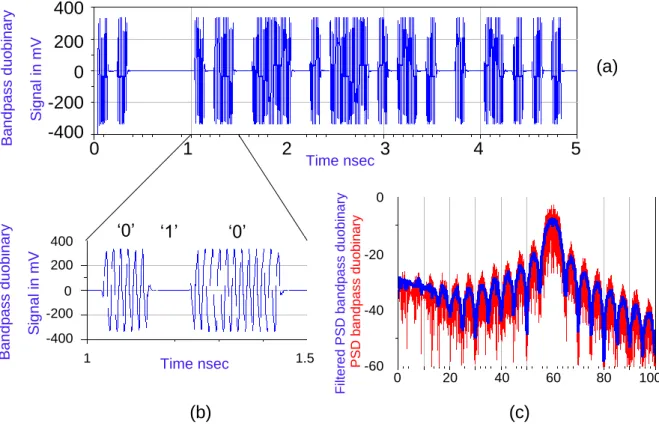
Figure II.17 : (a) Pass-band duobinary domain signal. (b) phase reversal in time-domain passband duobinary signal. (c) PSD and filtered PSD of a duobinary passband signal. ... 58
Figure II.18 : RF Mixer spectral components. ... 60
Figure II.19: Downconversion of third-order IM products [19]. ... 61
Figure II.20: Third-order intercept point and 1-dB compression points [20]. ... 62
Figure II.21 : (a) Basic active mixing cell. (b) Basic Gilbert cell. ... 63
Figure II.22 : (a) double-balanced diode ring. (b) Transistor ring passive mixer. ... 64
Figure II.23: Basic oscillator feedback circuit. ... 64
Figure II.24 : Phase-Locked loop architecture. ... 65
Figure II.25 : Oscillator phase noise. ... 66
Figure II.26 : Effect of phase noise. ... 66
Figure II.27 : Diode envelope detection scheme. ... 67
Figure II.28 : Square low demodulator. ... 67
Figure II.29 : AM modulated signal. ... 68
Figure II.30 : (a) ASK and OOK modulations. (b) ASK demodulator. ... 69
Figure II.31 : (a) Microstrip line principle. (b) Electric and magnetic fields. ... 70
Figure II.32 : Main transmission lines topologies. ... 71
Figure II.33: Block diagram representation of the proposed transceiver. ... 73
Figure II.35 : (a) Duobinary architecture. (b) Duobinary time-domain waveforms. (c)
Duobinary frequency-domain spectrum. ... 75
Figure II.36 : The transmitter modulated output waveform. ... 75
Figure II.37 : Demodulation time-domain waveforms and frequency-domain spectrum. ... 76
Figure II.38 : Demodulated 10Gbps signal eye diagram. ... 76
Figure II.39: Budget link analysis. (a) for a 15mm channel. (b) for a 5mm channel. . 78
Figure II.40 : Output signal eye diagram. (a) after a 5-mm transmission line. (b) after a 15-mm transmission line. ... 78
Figure II.41 : The proposed architecture for length adaptive serial link. ... 79
Figure II.42 : Impact of the transmitter mixer LO-RF isolation on the SNR. ... 79
Figure II.43 : Effect of the low-pass filter 3-dB cut-off frequency on the SNR. ... 80
Figure II.44 : Time-domain waveform and eye diagram of the output signal for different low-pass filter 3-dB cut-off frequencies. (a) 𝑓3𝑑𝐵 = 5 𝐺𝐻𝑧. (b) 𝑓3𝑑𝐵 = 10 𝐺𝐻𝑧. (c) 𝑓3𝑑𝐵 = 20 𝐺𝐻𝑧. ... 81
Figure II.45 : (a) eye diagram. (b) Total jitter histogram. (c) Jitter bathtub curves. ... 82
Figure III.1 : Conventional Bulk CMOS and FD-SOI transistors. ... 87
Figure III.2 : The threshold voltage variation for RVT and LVT 28nm FD-SOI technology [1]. ... 88
Figure III.3 : BEOL of the 28nm FD-SOI technology. ... 89
Figure III.4 : Transmission lines simulations for different technology nodes. (a) simulation model and (b) simulated attenuations. Orange, red, green, and blue refers to BiCMOS 55 nm CMOS 28 nm FDSOI, CMOS 40 nm, and CMOS 65 nm, respectively. [2] ... 89
Figure III.5 : M1 full and meshed ground plane for process compliance. ... 90
Figure III.6 : The ground plane in different metal layers. (a) the ground plane in M1. (b) the ground plane in B1. (c) the ground plane in IA. ... 91
Figure III.7 : The attenuation for a 50Ω microstrip when its ground is placed in M1, B1, or IA (EM simulation results). ... 92
Figure III.8 : The spacing between edge-coupled microstrips impact on the differential impedance 𝑍𝑑𝑖𝑓𝑓 and the attenuation in dB/mm (EM simulation results). ... 92
Figure III.9 : (a)The layout of the lines to reduce the used area and its cross-section layout. (b) The transmission lines insertion losses in dB (EM simulation results). (c) Layout respecting the ground plane density requirements. ... 93
Figure III.10 : Block diagram of the transmitter implemented in the prototype chip. . 94
Figure III.11 : Clock buffer AC-coupled inverter with resistive feedback. ... 95
Figure III.12 : Gain of the terminated AC-coupled inverter with resistive feedback shown in Figure III.11, for different feedback 𝑅𝐹values. ... 95
Figure III.13 :(a) Conventional differential precoder. (b) Differential precoder proposed in [6] (c) Used differential precoder. ... 96
Figure III.14 : (a) Duobinary modulator. (b) input and output modulated signals. ... 97
Figure III.15 : (a) A passive double-balanced mixer. (b) the output of a passive mixer. ... 98
Figure III.16 : (a) One transistor passive mixer 𝑅𝑂𝑁 and 𝑍𝑂𝐹𝐹. (b) Outputs of the duobinary modulator for different gates (AND and NOR) or ( NAND and OR). ... 98
Figure III.17 : The conversion gain of the mixer with respect to frequency and input power. ... 100
Figure III.19 : Time-domain waveforms representing: OUT1 and OUT2 the outputs of the duobinary modulator. IN_TL1 and IN_TL2 the outputs of the mixer (input of the
transmission lines). ... 101
Figure III.20 : Layout of the LO input transmission lines. ... 101
Figure III.21 : (a) Layout of a shielded RF pad. (b) The layout of a non-shielded RF pad [2]. (c) The simulated parasitic capacitance of a non-shielded RF-pad. ... 102
Figure III.22 : The return loss at the inputs of the transmitter for the LO+, DATA, and CLOCK inputs. ... 102
Figure III.23 : Block diagram of the receiver. ... 103
Figure III.24 : Schematic of the demodulator. ... 104
Figure III.25 : Implemented L1 inductor (Surrounding and dummy metals not shown). ... 105
Figure III.26 : (a) Symmetrical layout for the input signals. (b) Inductance and quality factor values. ... 105
Figure III.27 : Receiver input return loss. ... 106
Figure III.28 : (a) Basic current mirror. (b) Current mirror with inductive compensation. (c) Current mirror with resistive compensation. ... 107
Figure III.29 : Impact of the resistor on the CM bandwidth. ... 108
Figure III.30 : The CM resistor compensation technique impact on the output time-domain waveform. ... 108
Figure III.31 : Output return loss in dB. ... 109
Figure III.32 : Simulated system input and output waveforms. ... 110
Figure III.33 : (a) 10Gbps Eye diagram. (b) Eye diagram vertical histogram. ... 110
Figure III.34 : 10Gbps Bathtub curve. ... 111
Figure III.35 : (a) Layout of the receiver (not all the layers are included). (b) The core of the receiver(not all the layers are included). ... 112
Figure III.36 : (a) Time-domain output signal. (b) Output eye diagram. ... 113
Figure III.37 : (a) 14Gbps bathtub curve. (b) Eye diagram vertical histogram... 113
Figure III.38 : Schematic of the demodulator for digital applications. ... 114
Figure III.39 : (a) Time-domain output signal. (b) Output eye diagram. (c) Bathtub curve. ... 115
Figure A : Prototype chip in 28nm FD-SOI technology. ... 120
Figure B : The Xilinx 2.5D FPGA Product. ... 121
Figure C : (1) Top view of the 2.5D multi-core system with a 64-core CPU chip in the center with four DRAM stackes placed on either side of the multi-core die. (2) Side view of a simple interconnect implementation minimizing usage of the interposer. (3) The multi-core NoC slice uses a mesh topology. (4) Side view of a NoC logically partitioned across both the multi-core die and an interposer. (5) Interposer-layer NoC mesh. [4] ... 123
Figure D : Examples of possible system applications. ... 123
Figure E : Group delay of a wire. ... 124
Figure F : Differential characteristic impedance 𝑍𝑜𝑑𝑑 and insertion loss of the 28-nm FD-SOI chiplet transmission line. ... 125
Figure G : 3D view of: (a) the μbump. (b) the μbump and the signal strips (the ground is not shown). (c) Differential mode insertion loss and group delay of the μbump. . 125
Figure H : Transmission lines configuration for ground in M1 or M5 and their attenuation constant. ... 126
Figure I : Differential mode insertion and return loss of the 7-mm long channel. .... 127
List of tables
Table I.1 : Advantages and challenges of differents emerging on-chip interconnects. 8 Table III.1 : Comparison of our simulation results to the state of the art. ... 116
1
Introduction
Context
The Internet, computers, telephones, and airplanes are all considered part of the man's greatest inventions. They made our life more comfortable and simpler; they made the world a small village. So what do they have in common? They were all enabled by electronics. Electronics is a stepping-stone towards a better future, a more civilized and cleaner future.
For the last century or so, engineers have innovated by putting more and more applications into smaller spaces. At the beginning of the mobile revolution, a mobile weighed 4.5kg and required a carrying handle; Nowadays, our smartphones weigh less than 200 grammes and can fit in our pockets; they also have a camera (or several), a GPS, and some powerful CPUs...
These fast developments are mainly due to the advancements in microelectronics, integrated circuits architectures, and design. In the past, circuits were integrated on a large board (PCB, for example); the pitches were large and required a sizeable surface. Nowadays, more and more components are integrated into the same integrated circuit and are placed as close as possible. This resulted in a significant increase in performance. It also opened the door to new architectures such as the system-on-chip (SoC) or chip-multiprocessors improvements, where several functionalities are placed into the same integrated circuit (a CPU and its memory, for example); and are connected using an efficient on-chip communication network. The on-chip communication substantially impacts the chip performances, including its maximum speed, cost, reliability, and power consumption.
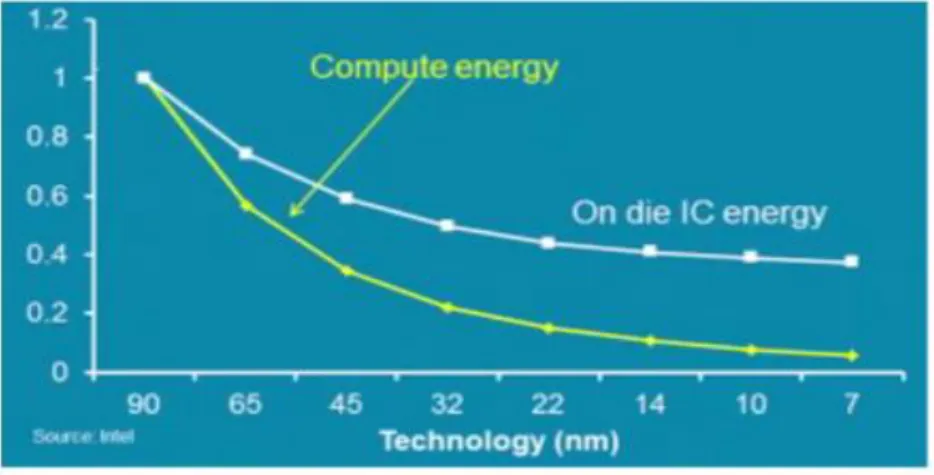
Intel predicted that communication energy efficiency would become the main challenge in more advanced nodes ICs. The interconnect energy is scaling slower than the computation energy within integrated circuits. Hence, the data movement on-die energy will dominate, as shown in Figure 1.
Figure 1 : Compute energy vs total on die IC energy for technology nodes.
Researchers have been working on several approaches to optimize the different metrics, either at the system level by proposing new architectures or at the devices
2
level by changing the used materials for wires, for example. Usually, trade-offs are required to meet different constraints.
One of the crucial steps toward optimized SoCs was developing Network-on-chips (NoC) solution; Before NoCs, designers relied on shared global buses to transmit the data; this approach was sufficient for up to ten cores single chip. However, as the chips kept growing and implementing extra functionalities, the shared global bus approach showed its limits and began to crumble. Mainly due to the wire's limitations on latency and overall speed of the chips.
NoCs, by design, allows for a larger number of cores and multiple communications at one time; they rely on routers to direct the signal from one point to the other, routers are connected through wires, similar to a traffic grid. In other words, the NoC connects different isolated IP blocks and defines the communication fabric/structure within the die; it also impacts its limits significantly. A poorly designed NoC will result in routing congestion and timing issues.
Fortunately, new NoC architectures or new topologies are popping up to handle different constraints and develop the quality-of-service with the increasing performance demands. In this work, we will propose a solution that may reduce the routing congestion within ICs, improve their performances, and help bring new architectures to light. One might imagine that the link developed in this work may be used for large ICs critical (timing) path or to place the memory further away from the CPU.
Motivation
Our work will not replace the standard wires solutions massively used nowadays. Instead, we propose it as a complementary solution to help solve some of the issues (especially timing issues) and extend the lifetime of the existing conventional NoC architectures for some time. We believe that the work proposed herein is most suitable for on-chip interconnects longer than two millimeters; because for distances lower than 2mm, the standard solutions are cost-efficient and more straightforward to implement.
Figure 2 : The proposed solution versus common interconnects distance range. Nowadays, large ICs require more and more long-range across the chip connections ( up to several millimeters); for example, the 2cm × 2cm processor shown in Figure 3, requires interconnects as long as 15mm to connect the chips borders. If only NoCs are used, the transmission takes several clock cycles to arrive; furthermore, going through all the routers, buffers... uses more resources than it should. For such long distances, optical interconnects seem like a reasonable option; however, they usually require more complex processes than simple ones, i.e., increases the cost.
Up to 2mm 20 mm and higher Distance 2 to ~20 mm Standard
solutions This solution
Optoelectronics interconnects
3
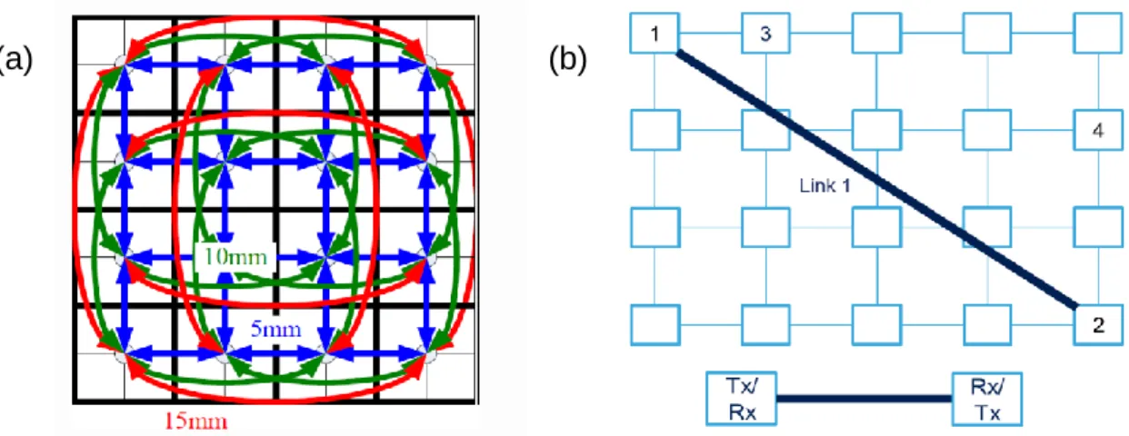
Figure 3: Possible usage applications of the proposed link. (a) Replace the long link in a NoC Torus topology with the proposed links.(b) Connect the furthest points directly.
The proposed approach's main benefit is to reduce the propagation latency (delay) of the wires. The propagation delay can be around 30 -40 ps/mm and higher in the standard solution, but it grows quadratically with the standard wires' length. In the used approach herein, the delay is linear and is around 7-8ps/mm. It is clear that the interest of this solution rises with distance. This link can be used to connect the edges of the chips creating high data rates fast links, as shown in red or green in Figure 3.a. This topology is similar to the standard Torus NoC topology; We propose to replace the long slow links with this fast links to improve the performances. If designed correctly, they can also connect the two furthest points on a die, as shown in Figure 3.b. Thus, the data sent through these links will not go through the NoC routers and switches; it will reduce their congestion and provide a back-up link to retransmit lost data, for example.
One of the main issues in communication systems is distortion due to the channel's physical properties such as the channel's dispersive nature, where the frequency components propagate at different velocities, or an increase in the channel's attenuation coefficient due to the skin effect, for example. This usually causes the pulse traveling through the channel to decrease in amplitude and spread in the time domain. Several methods have been carried out in order to solve these issues. Equalization was used to reduce the channel's frequency selectivity by reversing the distortion; Then reconstructing the initially transmitted signal.
However, the complexity and power consumption of the equalizers dramatically increased in the last years. The equalization approach was attractive with the transistor and voltage scaling, which is not optimal anymore since voltage scaling is slowing down.
In this work, we do not require equalization, since as it will be shown, the transmission lines do not suffer from such effects at higher frequencies; Thus, they provide a good medium for transmission with minimal distortion, and we will show that we achieved a BER lower than 10−12up to 14Gbps data transmission.
Furthermore, we used bandpass duobinary modulation to take full advantage of the available bandwidth; Duobinary modulation is more efficient as it compresses the spectrum of the signal by a factor of two, and thus use a two time smaller bandwidth. This compression can also be translated into more relaxed design constraints on the RF components (linearity...) compared to an ASK modulation. In addition,
4
coherent demodulation is used relying on a simple power detector without any need for a carrier in the receiver. We designed a 10Gbps prototype chip, and we used the advanced 28nm FD-SOI technology from STMicroelectronics to design the transmitter, the channel, and the receiver. We will show that we doubled the state of the art data rate with comparable energy efficiency and signal integrity.
Thesis outline
This thesis is organized as follows:
-We start the first chapter by introducing the standard on-chip interconnect solutions and the emerging solutions such as the wireless solution (WiNoC), the optical solution (ONoC), and the radiofrequency interconnect (RF-I). Next, we discuss the different solutions, share their advantages and challenges; then, we dive more into the standard wires solution and its limitations for long-range links. We also explain the chosen RF interconnects approach and show its advantages (mainly delay) as well as its state of the art works.
-In the second chapter, we will introduce some common modulation schemes and the duobinary modulation. Next, we study the duobinary modulation, show its implementation and main issues. Next, we show the proposed system architecture and study the adaptive length approach where the transmitter and receiver can be used for different link lengths without redesign.
-In the third chapter, we will focus on the circuits implementations. Firstly, we start with the channel choice and its EM simulation results; Secondly, we present the 10Gbps transmitter and receiver simulation results; As well as its performances up to 14Gbps. Next, we show its simulation results for a more practical case with buffers at its output. Finally, we compare our results to the state of the art results.
Finally, we conclude and propose some perspectives to develop this approach and use it for different applications such as interposer interconnects.
5
Serial Links overview
Every day, researchers innovate to meet future performance requirements in different fields (medical, automotive, telecommunications...); In recent years, our life changed because of such innovations and will continue to change as long as we push the limits. Microelectronics is driving these developments as engineers continue to make smaller and more power-efficient devices to unblock the bottlenecks. In integrated circuits, interconnects are considered as a bottleneck that we are facing nowadays. In this chapter, we introduce the emerging on-chip interconnects. We discuss the existing on-chip interconnects, their issues, and their main parameters, but also the standard solution used for the last decades. Finally, we introduce the RF-interconnect state of the art, one of the emerging RF-interconnects solutions.
I.AN INTRODUCTION INTO EMERGING ON-CHIP INTERCONNECTS ... 6
II.HIGH SPEED SERIAL LINK ARCHITECTURE ... 9
II.1. Line coding ... 10 II.2. Bandpass modulation ... 11
III.SERIAL LINK PERFORMANCE METRICS ... 11
III.1. Eye Diagram ... 11 III.2. Bit error rate ... 12 III.3. Error Vector Magnitude ... 13 III.4. Inter-symbol interference ... 14 III.5. Jitter ... 14 III.6. Error correcting codes ... 17
IV.ON-CHIP INTERCONNECTS ... 18
IV.1. RLCG model ... 18 IV.2. RC wire ... 23 IV.3. Transmission lines ... 34
V.RF-INTERCONNECT STATE OF THE ART ... 37 VI.CONCLUSION ... 42
6
I.
An introduction into emerging On-chip Interconnects
Over the past decades, the market demanded higher performances, lower power consumption along with lower integration cost. This was possible due to the CMOS technology scaling where digital gates size decreased at a fast rate, which lead to a reduction of gate delay and silicon areas [1]. Today's transistors are at least 20 times faster and occupy less than 1% of the area of those built 20 years ago.
Due to this progress, numerous functions are now integrated on the same chip. Each function typically requires one or several cores or devices. Thus, the number of integrated cores inside systems-on-chip (SoC) grew significantly, which lead to the adoption of Networks-on-chip (NoC) as a communication network in large integrated circuits [2]. An example is shown in Figure I.1, the message is relayed from one IP core to the other through a network of routers and network interfaces.
Figure I.1 : Architecture of a typical NoC.
Chips Multi-Processor (CMP) [3] was proposed by the research community to take advantage of this scaling. The area of each processor core is reduced then multiple cores are integrated on the same chip to take advantage of high parallelization. It is clear that as the number of processor cores and memory increases, the rate of communication increases significantly. Thus, the number of required interconnects to connect different IPs raises too [4].
The research community has been working on different solutions to overcome on-chip communications challenges, such as 3D integration [5]. 3D integration adds an extra dimension for interconnection, and thus shorter distances are required, i.e., long interconnects used in 2D structures are replaced by vertical interconnects. For example, critical path gates can be placed very close to each other by stacking them and connecting them in the Z direction.
While 3D solutions are up-and-coming, 2D solutions are still prominent and still have a lot to offer without added complexity and cost. Besides improving the standard 2D wire signaling techniques, researchers proposed several solutions such as optical interconnects (ONoC) [6], wireless interconnects (WiNoC) [7], and radiofrequency interconnects (RF-I) [8]. Each solution comes with its advantages and challenges and might be optimal for specific applications.
7
The standard on-chip metal wire was used for a long time because it was cheap; moreover, its delay and power consumption were acceptable. These wires, also known as RC wires, are characterized by there dominant resistance and capacitance, the signal is transmitted by charging/discharging the wire [9]. RC wires delay is proportional to the inverse of the capacitance and resistance of the wire. Furthermore, it grows quadratically with length; thus, the delay will significantly increase for long-range distances. One solution to lower the latency is to use larger wires. Larger wires have smaller resistance values at the cost of a lower ratio of bit per area, i.e., reducing data throughput per surface. RC wires will be discussed in detail in section IV.2.1.
Researchers investigate optical interconnects for on-chip interconnects, it is a more radical approach to solve the expected long-range interconnects bottleneck. Adding an extra layer of optical interconnects offers a high bandwidth per channel; the transmitted signal can cross long distances with low latency due to the speed of light propagation; these interconnects are immune to electromagnetic noise. This approach is practical for clock distribution as it reduces the clock skew, as shown in [10]. One example of these links was shown in [11], where they designed an optical intra-chip link at 10Gbps per channel; they achieved a total data throughput of 100Gbps by multiplying the number of links 10x10Gbps.
Optical interconnects are very promising for long-range on-chip interconnects, but they face various vital challenges [6], [10]. Firstly, complexity because optical circuitry requires large areas and non-friendly CMOS processes. Power consumption and thermal regulation are an essential challenge. Even though the channel losses are negligible, the power consumption of current optical devices, e.g., light sources, modulators... required to generate the signal is significant. Thus, from a power consumption view, the optical solutions will only be interesting for long-range communications, the distance at which they become optimal has still to be defined. To summarize, optical solutions will be used more often once they become CMOS manufacturing and assembly processes friendly, and with a high yield. Furthermore, to become financially attractive, their cost should be reduced.
Another approach is to use wireless interconnects, also known as wireless NoC (WiNoC) [7]. This approach transmits the signal as an electromagnetic signal using on-chip antennas. Thus, this solution can connect all adjacent nodes with very low latency, taking advantage of the shared medium of transmission. The scaling of transistors enables the use of higher carrier frequencies and thus avoid transmitting in the currently occupied spectrum. Higher frequencies in the mmWave range require small integrated antennas [12], and researchers are striving to design efficient wideband antennas at these high frequencies [7], since the antenna bandwidth is the limiting factor in this approach. Implementation in the THz range is also interesting because of large available bandwidth and small antennas, but the CMOS transistors cut-off frequency becomes the limiting factor in this case. Furthermore, a multi-carrier transmission will require different antennas with different center frequencies resulting in significant area overhead.
Instead of free space signal propagation, waveguided propagation can be used to transmit the signal. This approach is called RF interconnects (RF-I) [3], [8] and uses low-loss transmission lines (TL) to propagate the high-frequency signal over long distances. This solution uses the standard CMOS processes, and do not require any changes. Moreover, it benefits from faster transistors due to CMOS scaling. It offers a
8
low-latency transmission since the signal travels along the TL at the effective speed of light in 𝑆𝑖𝑂2.
Furthermore, when using TL, a large bandwidth is available, allowing for high data rates transmission with minimum distortion. To reduce the attenuation, the lines are implemented using the higher metals in the BEOL (Back End Of Line) stack because of their thickness. But also, the TLs require wide wires, which means that the number of these links is limited. Another challenge to consider is the crosstalk between these lines, i.e., the lines should not be placed too close to each other to avoid coupling. The dimensions of the TLs and the spacing between them limits the interconnect density. Thus the efficiency of each link should be improved to reach a higher total data throughput.
The RF-I approach is more power-efficient than the standard wire solution for long-distance links, due to the low attenuation of the transmission lines. The standard solution uses power-consuming repeaters to regenerate the signal periodically; longer distances require more repeaters.
In this work, we will discuss the standard wire solution briefly, and we will focus on the RF-I solution since we believe it is not efficiently used yet, and better performances can be reached.
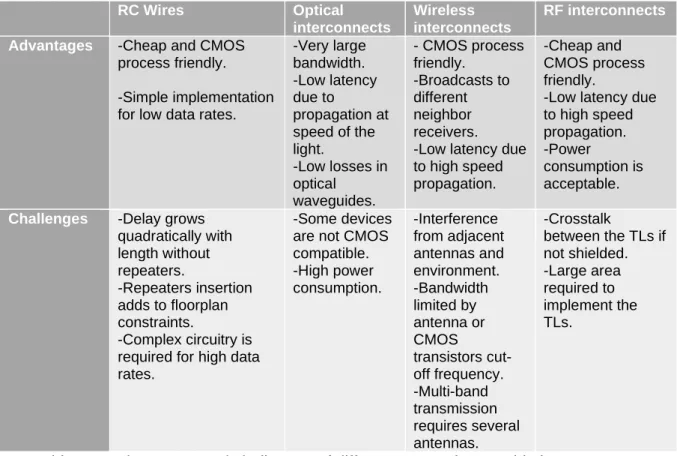
The previously techniques mentioned are different, and none of them is ideal, each method has its advantages and drawbacks that might be suited for unique applications and uses. For example, wireless propagation (WiNoc) is suitable for broadcasting to all receivers. Or use optical solution and RF-I when the latency is critical. And lastly, use the standard wire solution for short distances where the other solutions will not be suitable. Table I summarizes the different approaches, advantages, and challenges, but a more detailed comparison can be found in [13].
RC Wires Optical interconnects
Wireless interconnects
RF interconnects Advantages -Cheap and CMOS
process friendly. -Simple implementation for low data rates.
-Very large bandwidth. -Low latency due to propagation at speed of the light. -Low losses in optical waveguides. - CMOS process friendly. -Broadcasts to different neighbor receivers. -Low latency due to high speed propagation.
-Cheap and CMOS process friendly.
-Low latency due to high speed propagation. -Power
consumption is acceptable. Challenges -Delay grows
quadratically with length without repeaters. -Repeaters insertion adds to floorplan constraints. -Complex circuitry is required for high data rates.
-Some devices are not CMOS compatible. -High power consumption. -Interference from adjacent antennas and environment. -Bandwidth limited by antenna or CMOS transistors cut-off frequency. -Multi-band transmission requires several antennas. -Crosstalk between the TLs if not shielded. -Large area required to implement the TLs.
9
II.
High speed serial link architecture
A typical high-speed serial link includes three main elements, a transmitter (TX), a channel, and a receiver (RX). In a serial link, most of the signal integrity issues are due to the channel's low-pass response, making the transmitted signal sometimes unrecognizable to the receiver. Ideally, a transceiver should transmit and recover the data without errors, use a small area, and consume very little power.
The transceiver's complexity depends on several parameters, such as the channel properties, the expected data rates, and the allocated power budget. Usually, designers compromise on one of several parameters to achieve the specifications.
Figure I.2 shows the architecture of a typical high-speed serial link. The transmitter multiplexes low-speed parallel data into a high-speed serial stream and then transmits it through the channel. To increase the data quality and consequently the data rates, designers use equalizers and pre-emphasis techniques in the transmitter (or the receiver) to compensate for the channel's imperfection, such as frequency-dependent losses.
Figure I.2 : Architecture of a typical high-speed serail link.
Equalization is performed at both ends of the transceiver when the channel degrades the signal severely; for example in RC Wires cases. Hence, when the signal arrives at the receiver, it goes through an equalization stage before sampling. Sampling the received data at the proper rate is crucial for a reduced number of errors. However, in most high-speed serial links, the clock is not transmitted. Therefore, the receiver needs to recover the clock to sample the data accurately. In other words, detect the most suitable sampling location in a jittery signal to produce a correct signal.
High-speed serial links use a Clock Data Recovery (CDR) to regnerate the clock from received data, then uses the recovered clock as the reference to trigger a retiming flipflop to clean up the incoming data as shown in Figure I.3.
Figure I.3 : Clock recovery and data retiming for a CDR circuit. T X TX TX Equalization T RX Equalization X Channel
10
The complexity of the CDR circuitry depends on the link type. We can distinguish two types of links: source-asynchronous and source-synchronous systems.
A serial link is called source-synchronous when both the TX and RX use the same clock source. For this type of link, the CDR only provides a finite phase capturing range and requires a lower complexity.
However, most of wireline serial links belong to the second category and are called source-asynchronous. For this link, the TX and RX use different clock sources, which results in a frequency offset between the received data and the RX local clock, and thus increases the complexity of the needed CDR. The CDR usually drives several transmitters and receivers for efficient use of the area and power. The CDR clock can also be used to drive the equalizers.
As we will see in the equalization techniques section, most of the equalizers are discrete-time equalizers that require a clock. Thus, equalizing at both TX and RX means that a clock should be available at both ends.
Researchers proposed a wide variety of CDR architectures based on Phase-locked loop (analog and digital) and delay-Phase-locked loop (DLL) amongst different designs. These architectures will not be discussed in this work. However, the authors in [14] provided an overview of these architectures.
Line coding
Line code is the code used to transmit digital data over a channel such as an RC wire or a TL. These codes are used to convert a sequence of bits into a digital signal, and efficiently use the channel's bandwidth to reduce noise and interference. Line codes cover unipolar, polar, bipolar signals, and multilevel signals. Each can be divided into subcategories, but the most common ones are the Non-Return to Zero (NRZ) and Pulse amplitude modulation (PAM). Figure I.4 shows an example of unipolar Return to Zero (RZ) and NRZ signals; the binary states are easily distinguishable in the transmitted sequences,i.e., the presence of a signal is equivalent to a binary '1'; its absence is a binary '0'. Square signals are preferred because their generation and detection processes are simple, especially that most of the logic digital circuits function in a two-states approach, i.e., on and off. However, analog signals do not follow the same rule, and they can take an endless variety of forms.
Choosing the appropriate code depends on several factors, such as the presence or absence of DC component, simple regeneration, and power efficiency [15].
11
Bandpass modulation
Bandpass modulation [15] techniques modify the shape of a carrier wave (usually sinusoidal) to encode the transmitted data; In other words, shift the signal up in frequency. In this case, the spectral magnitude is nonzero in the band around the carrier frequency and is negligible elsewhere. This transmitted data is a baseband waveform (analog or digital) and is called the modulating signal. For example, it can be the NRZ or RZ signals shown in Figure I.4. This technique is useful for a channel that acts as a bandpass filter, for shared channels where only certain frequency bands are available. We can distinguish three categories of modulation: amplitude, frequency, and phase modulation. The carrier's amplitude is varied in proportion to the data signal in amplitude modulation; While its phase is varied in phase modulation. Newer modulations called Quadratic Amplitude Modulations (QAM) combine amplitude and phase carrier modulations to define more symbols in the constellation, increasing the data rate with the same bandwidth. In frequency modulation, the frequency of the signal is altered in proportion to the data.
The inverse operation is called demodulation, and it consists of recovering the data from the carrier at the far-end, usually the receiver. Each modulation has its advantages/disadvantages that fit specific applications.
III.
Serial link performance metrics
In serial links design, compromising between the different parameters is essential, although some metrics are more critical than others. These include data rates; The data rate of a serial link is defined as a the number of bits transferred per second. To satisfy the need for high data rates, serial links advanced from several Gbps to several tens of Gbps, at the cost of complexity and power consumption. Hereafter, we introduce the main tools and metrics a designer uses to identify whether a transmission is reliable or not.
Eye Diagram
Useful tools such as eye diagram are used to visualize high-speed serial links signals in time domain. An eye diagram [16] indicates the quality of the signals transmitted, and is generated by overlapping successive waveforms corresponding to the received signal. These waveforms can be the bits of a long data stream.
It is a very powerful tool that allows the designer to intuitively interpret the quality of the signal, by looking at the area in the middle of the eye diagram named the "eye" or eye-opening. The eye closes vertically if the signal-to-noise-ratio (𝑆𝑁𝑅) is degraded, mainly due to noise and Intersymbol-interference (𝐼𝑆𝐼). Signal to Noise ratio (𝑆𝑁𝑅) is simply the ratio of the power of a signal to the power of the noise and is generally expressed in decibels (𝑑𝐵).
The noise is identified at the top and bottom lines of the eye. Thicker lines are an indicator of the presence of more noise. Thus, if the eye closes vertically, the detection of different states becomes difficult.
12
Figure I.5 : An Eye diagram.
Bit error rate
Another critical metric is the number of error bits per transmitted bits. Bit error rate (𝐵𝐸𝑅) is one of the popular metrics used to assess the performance of a communication system and prove the reliability of the data transmission. 𝐵𝐸𝑅 indicates the rate at which errors occur in a transmission system, it can be calculated by comparing the transmitted sequence of bits to the received bits and counting the number of errors. Or in other words, it is the ratio of the number of error bits over the total received bits as given by:
𝐵𝐸𝑅 = 𝑁𝑏𝑟 𝑜𝑓 𝑒𝑟𝑟𝑜𝑟𝑠
𝑇𝑜𝑡𝑎𝑙 𝑛𝑢𝑚𝑏𝑒𝑟 𝑜𝑓 𝑏𝑖𝑡𝑠 𝑠𝑒𝑛𝑡= 𝑁𝑒𝑟𝑟
𝑁𝑏𝑖𝑡𝑠 (I-1)
If the link between the transmitter and receiver is good i.e. no noise or jitter, then this value will be very small. In serial links. In practice, the number of bits sent 𝑁𝑏𝑖𝑡𝑠 is chosen depending on the 𝐵𝐸𝑅 threshold and its confidence level (𝐶𝐿). 𝐶𝐿 is the percentage of tests that the system's true 𝐵𝐸𝑅 (if 𝑁𝑏𝑖𝑡𝑠 = ∞) is less than the 𝐵𝐸𝑅 threshold. The confidence level formula is given by:
𝐶𝐿 = 1 − 𝑒−𝑁𝑏𝑖𝑡𝑠∗𝐵𝐸𝑅 (I-2)
In standard wireline communications, a 𝐵𝐸𝑅 of 10−12 and a CL of 95% is often required to avoid using error-correcting codes. We should expect no errors if 3 × 10−12 bits are sent, if errors are detected the mathematical expressions can be found in [17].
As mentioned previously, noise and jitter can degrade the communication channel and its 𝐵𝐸𝑅. Figure I.6 shows the statistical relation between 𝐵𝐸𝑅 and the signal to noise ratio (gaussian noise) per bit 𝐸𝑏⁄𝑁0 for different types of modulations.
13
Figure I.6 : 𝐵𝐸𝑅 versus 𝐸𝑏⁄ 𝑁0for different modulations.
The normalized signal to noise ratio (𝐸𝑏⁄𝑁0), also known as 𝑆𝑁𝑅 per bit is usually used to compare digital modulations. It is the ratio of energy per bit (𝐸𝑏) to the
spectral noise density (𝑁0). The energy per bit 𝐸𝑏 is the signal energy of a single bit; it
can be computed by dividing the signal power by the bit rate; it is expressed in joules.
𝑁0is the noise spectral density (noise in 1𝐻𝑧 bandwidth); it is expressed in Joule per Hetz.
As mentioned previously, bit errors can be caused by amplitude noise degrading the 𝑆𝑁𝑅 or by to timing uncertainty,i.e., jitter. In this case the demodulator or receiver can detect the wrong bit, which may be the previous or the next bit.
Error Vector Magnitude
Error Vector Magnitude (𝐸𝑉𝑀) measures digitally modulated signal quality; it expresses the difference between the voltage of the expected symbol and the received one. 𝐸𝑉𝑀 provides extra information compared to 𝐵𝐸𝑅, where the 𝐵𝐸𝑅 reports the number of bits containing errors only. Constellation diagrams are used to visualize the demodulated signals and the 𝐸𝑉𝑀. A constellation diagram is a plot of symbols represented by their unique magnitude (and sometimes phase) voltage value.
Figure I.7.a represents a 16QAM constellation diagram, the constellation contains 16 unique symbols with different amplitudes and phases. Figure I.7.b represents measured 𝐸𝑉𝑀; the small dots on the diagram represent the errors in the measured symbols. Figure I.7.c shows a single error vector magnitude presentation; the error vector magnitude is the vector's length that connects the reference symbol position and the measured symbol position.
14
Figure I.7 : (a) Ideal constellation diagram. (b) Measured constellation diagram. (c) Single error vector manitude calculation.
Inter-symbol interference
Inter-symbol interference (𝐼𝑆𝐼) is a form of signal distortion that happens when one symbol interferes with previous or subsequent symbols, it is caused mainly by the dispersion of the channel and its finite bandwidth, the majority of interconnect channels have a low-pass frequency response. Passing a signal through such channel results in attenuation of the high-frequency components, furthermore, in such a medium the signal components will travel at different speeds and thus arrive at different moments. The distortion of the channel results in the pulse spreading out and interfering with its previous symbols, as shown in Figure I.8. Thus, depending on when the pulse is sampled, the receiver can make the wrong decision. The performances and reliability of these links depend on several figures of merit such as bit error rate.
Figure I.8 : Inter-symbol interference.
Jitter
The eye diagram in Figure I.5 closes horizontally if the jitter increases. The eye diagram is rich in information and can be further utilized to extract the jitter histogram, and the Total jitter 𝑇𝐽.
Jitter is the temporal deviation of the signal from its ideal value at a certain point, as shown in Figure I.9.
Ideal constellation Diagram. Measured constellation Diagram. Q Q I I
15
In digital transmissions, the jitter is defined at the transition from 0/1 and 1/0, and it can be written as 𝑡 = 𝑇 + 𝜑 where t is the time of the transition, 𝑇 its ideal position and 𝜑 the time offset of the transition also called timing jitter.
Figure I.9 : Waveform timing variations.
In analog transmissions, jitter is known as phase noise given by:
𝑆(𝑡) = 𝑃(𝑡 + 𝜑(𝑡)), (I-3)
where 𝑆(𝑡) is the jittered signal, 𝑃(𝑡) the ideal signal, and 𝜑 (𝑡) the phase noise. The jitter is defined either using time units ( 𝑝𝑠 and 𝑛𝑠 ) or in unit interval [UI]. The UI is the proportion of total jitter 𝑇𝐽 per bit and is given by:
𝐽𝑖𝑡𝑡𝑒𝑟(𝑈𝐼)= 𝑇𝐽
𝑇𝑏𝑖𝑡 , (I-4)
The total jitter is decomposed into two main categories: Random jitter (RJ) and Deterministic jitter (DJ) as shown in Figure I.10.
Figure I.10 : Jitter components [17].
Random jitter covers the unpredictable noise introduced randomly by thermal noise, shot noise, or "Pink" noise in the circuits. It is described probabilistically and usually follows a normal distribution. In theory, it is a constant value generally expressed as the root mean square (𝑟𝑚𝑠) value equivalent to its standard deviation 𝜎. The 𝑟𝑚𝑠 random jitter 𝑅𝐽𝑟𝑚𝑠 derived from the standard deviation can be converted to a peak-to-peak 𝑅𝐽𝑝𝑝 using the formula given by:
16
This formula relates the 𝑅𝐽𝑝𝑝to 𝑅𝐽𝑟𝑚𝑠through a BER function, 𝑁(𝐵𝐸𝑅) depends on the required 𝐵𝐸𝑅. for a 𝐵𝐸𝑅 of 10−12, 𝑁(𝐵𝐸𝑅) is equal to 14.069.
Figure I.11 : Typical waveform including 𝑅𝐽, and 𝑅𝐽 Histogram[19].
Deterministic jitter represents the jitter with an identifiable and predictable source. Its peak-to-peak value is bounded with a well-defined minimum and maximum. As shown in Figure I.10, deterministic jitter covers data-dependent jitter (𝐷𝐷𝐽) and bounded uncorrelated jitter (𝐵𝑈𝐽). Each component can be decomposed to subcategories to diagnose the causes of the jitter more precisely.
Figure I.12 : (a) Dual dirac method . (b) Typical 𝐷𝐽 Waveform, and histogram[19]. To rapidly estimate 𝑇𝐽 [20] the sum of 𝐷𝐽 and 𝑅𝐽, dual dirac method is used.This method describes 𝑇𝐽 as two Dirac delta functions convolved with a gaussian function, the distance between 𝜇𝐿 and 𝜇𝑅 is the deterministic jitter 𝐷𝐽(𝛿𝛿), while the dashed lines shown in Figure I.12.b represent the random jitter.
The advantage of this model is that it does not require to calculate the different components of deterministic jitter individually. The formula for 𝑇𝐽 as a function of 𝑅𝐽 and 𝐷𝐽 is given by:
𝑇𝐽(𝐵𝐸𝑅) = 𝑁(𝐵𝐸𝑅) ∗ 𝑅𝐽𝑟𝑚𝑠+ 𝐷𝐽(𝛿𝛿), (I-6)
(a)
17
To evaluate the 𝑆𝑁𝑅 and the jitter in a system quickly, engineers use eye diagram and bathtub curves.
Figure I.13 : a bathtub plot showing the BER as a function of sampling point delay. Another powerful tool to analyze jitter is the bathtub plot [21]; This plot can be used to determine the acceptable total jitter in the system for a specific 𝐵𝐸𝑅.
The bathtub plot is shown in Figure I.13. It represents the 𝐵𝐸𝑅 versus sampling point within the unit interval. We can distinguish three regions, the deterministic jitter region, the random jitter region where the 𝐵𝐸𝑅 falls rapidly, and the third region is the eye-opening. To open the “eye” and improve the 𝐵𝐸𝑅, designers use several techniques such as equalization to counter the channel distortion effect, or error correcting codes, these techniques are often combined.
Error correcting codes
Error correcting codes [15] (ECC) was introduced by Hamming [18] in the '40s, and has been crucial since then for telecommunications systems that cannot re-send the message, such as interplanetary communication; Or for when a 100% reliable system is not affordable i.e. a less reliable system combined with ECC costs less.
In this approach, a portion of the signal bandwidth can be exchanged for a better transmission fidelity, when the communication channel is noisy or unreliable, redundant information is added to the original data; these extra bits allow the detection and correction of the errors if they exist.
We can distinguish two types of ECC; the first type is called block codes where the correction bits are added as a block at the end of the original bitstream; for this type of ECC the original bitstream must have a fixed length. The second type is called convolutional codes, where the correction bits are added continuously into the bitstream. Furthermore, contrary to the block code, the bitstream does not have a beforehand fixed length. However, these flexibilities of the convolutional codes compared to the block code comes at a complexity cost.
The code-rate of an ECC is the ratio between the code correction bits and the total number of bits (bitstream plus the code correction codes), a high code-rate means that high reliability is achievable. Still, it also means that a large number of bits are added to the original data. Thus, a tradeoff between data rate and channel reliability is always necessary.
18
IV.
On-chip Interconnects
In recent ICs, on-chip global signaling became a bottleneck for the required data rates. Firstly, due to the production of larger chips, which leads to longer links. But also due to the wire pitch decreasing in smaller nodes [1], which significantly increases the resistance and increases the parasitic capacitance due to the dense routing.
In the first stages of the design process, to connect the nodes and devices, we usually use ideal wires that show no attenuation or latency. This first approach is not wrong, since modeling all wires is too complicated, and depending on the case, some parameters might be negligible compared to more dominant parameters. For example, for a wire with small cross-section, the inductance can be neglected since the resistance will be more significant. Hence, a quick review of on-chip wires main properties is desirable; we will use first-order models to understand these effects.
RLCG model
Wires are used to transmit energy from one point to another using two conductors or more; its source is usually TX driver and load RX. The term transmission line can be used for any structure that guides an electromagnetic wave; its parameters are usually optimized to avoid wasting energy during the transmission.
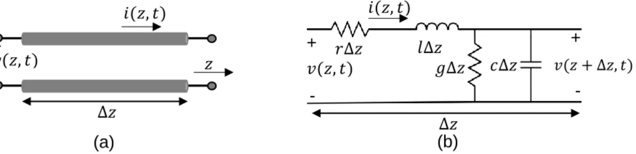
TL effects are not considered in low frequencies usually. However, at high frequencies, they affect the power transfer and are considered even for very short distances. In general, if a transmission line has a length higher than 1/16 of a wavelength, then the line length will significantly affect the circuit's impedance. Figure I.14.a shows a typical representation of a two-wire transmission line.
Figure I.14.b shows a uniform network distributed along the two-wire lines where each network represents an infinitesimal length ∆𝑧 of the line.
Figure I.14: (a) An incremental length of a transmission line. (b) Lumped-element model. When a signal is injected into the transmission line, it creates electrical and magnetic fields around the line. The energy stored in the electrical field between the line and its ground is modeled as a shunt capacitor 𝑐∆𝑧. The energy stored in the magnetic field around the line is called the series inductance 𝑙∆𝑧.
The series resistance 𝑟∆𝑧 represents the losses due to the finite conductivity of the transmission line. The shunt conductance 𝑔∆𝑧 represents the losses due to the non-ideality of the dielectric surrounding the TL.
𝑖(𝑧, 𝑡) 𝑣(𝑧, 𝑡) + - ∆𝑧 𝑟∆𝑧 𝑙∆𝑧 𝑔∆𝑧 𝑐∆𝑧 𝑣(𝑧, 𝑡) + - ∆𝑧 𝑣(𝑧 + ∆𝑧, 𝑡) 𝑖(𝑧, 𝑡) 𝑧 (b) (a) + -
![Figure I.26: Enhancing the high frequency components effect on the effective bandwidth [38]](https://thumb-eu.123doks.com/thumbv2/123doknet/14549860.725591/49.892.181.651.667.990/figure-enhancing-high-frequency-components-effect-effective-bandwidth.webp)
![Figure I.28 : Implementation of an active CTLE and its frequency response [42].](https://thumb-eu.123doks.com/thumbv2/123doknet/14549860.725591/51.892.206.756.114.366/figure-i-implementation-active-ctle-frequency-response.webp)
![Figure II.5 : NRZ and duobinary: waveform, eye diagram, and spectrum [10].](https://thumb-eu.123doks.com/thumbv2/123doknet/14549860.725591/71.892.227.675.443.678/figure-ii-nrz-duobinary-waveform-eye-diagram-spectrum.webp)
![Figure II.13 : (a) Proposed duobinary-to-binary converter [14]. (b) Circuit truth table (c) Duobinary signal as an eye diagram and a time waveform](https://thumb-eu.123doks.com/thumbv2/123doknet/14549860.725591/75.892.162.734.728.939/figure-proposed-duobinary-converter-circuit-duobinary-diagram-waveform.webp)