HAL Id: hal-01788355
https://hal-amu.archives-ouvertes.fr/hal-01788355
Submitted on 9 May 2018
HAL is a multi-disciplinary open access
archive for the deposit and dissemination of
sci-entific research documents, whether they are
pub-lished or not. The documents may come from
teaching and research institutions in France or
abroad, or from public or private research centers.
L’archive ouverte pluridisciplinaire HAL, est
destinée au dépôt et à la diffusion de documents
scientifiques de niveau recherche, publiés ou non,
émanant des établissements d’enseignement et de
recherche français ou étrangers, des laboratoires
publics ou privés.
Single Event Effects: the effects of Single particles on
electronics. Space, aerospace and ground
Jean-Luc Autran, Daniela Munteanu
To cite this version:
Jean-Luc Autran, Daniela Munteanu. Single Event Effects: the effects of Single particles on electronics.
Space, aerospace and ground. ANNIMA 2017, Jun 2017, Liège, Belgium. �hal-01788355�
Single Event Effects: the effects of Single particles on electronics
Space, aerospace and ground
J.L. Autran*, D. Munteanu*
Aix-Marseille Univ, CNRS, Univ Toulon, IM2NP (UMR 7334), Faculté des Sciences – Service 142, Avenue Escadrille Normandie Niémen, F-13397 Marseille Cedex 20, France
* The authors are also with the
Radiation Effects & Electrical Reliability (REER) Joint Laboratory IM2NP-STMicroelectronics
1. Introduction
The integrated circuit (IC) sensitivity to radiation coming from the natural space or present in the terrestrial environment has been found to seriously evolve [1-3] as MOSFET dimensions have reduced. Nowadays, for ultra-scaled devices, natural radiation is inducing one of the highest failure rates of all reliability concerns for devices and circuits in the area of nano-electronics [2]. In particular, ultra-scaled memory integrated circuits have been found to be more sensitive to single-event-upset (SEU) and digital devices more affected by digital single-event transient (DSETs). This sensitivity to Single Event Effects (SEE) is a direct consequence of the reduction of device dimensions and spacing within circuit blocks combined with the reduction of supply voltage and node capacitance, resulting in a decrease of both the critical charge (i.e. the minimum amount of charge required to induce a bit flip) and the sensitive area (i.e. the minimum collection area inside which a given particle can deposit enough charge to induce a bit flip) [2], [4].
This paper examines the issue of soft errors induced by natural radiation at ground level in current and future CMOS digital circuits. Four main topics will be addressed in the following:
• in a first part we briefly describe the natural radiation environment at ground and atmospheric levels;
• the physics and the underlying mechanisms of soft errors at silicon level are summarized a second part. We briefly depict the main mechanisms of interaction between atmospheric radiation and circuit materials and the electrical response of transistors, cells and complete circuits.
• the third part explains soft error characterization using accelerated and real-time tests, as well as modelling and numerical simulation issues. • the fourth part presents and discusses the radiation
response of advanced technologies, including deca-nanometer bulk, FD-SOI and FinFET families.
2. Natural radiation environment at ground and atmospheric levels
Soft errors are the result of the interaction of highly energetic particles, such as protons, neutrons, alpha particles, or heavy ions, with the sensitive region(s) of a microelectronic device or circuit. A single event may perturb the device/circuit operation (e.g., reverse or flip the data state of a memory cell, latch, flip-flop, etc.) or definitively damage the circuit (e.g. gate oxide rupture, destructive latch-up events). The problem has been well known for space applications over many years (more than forty years) and production mechanisms of soft errors in semiconductor devices by energetic protons, electrons and heavy ions well apprehended, characterized and modelled [5]. In a similar way for avionic applications, the interaction of atmospheric high-energy neutrons and protons with electronics has been identified as the major source of soft errors [6]. For the most recent deca-nanometers technologies, the impact of other atmospheric particles produced in nuclear cascade showers on circuits has been clearly demonstrated, in particular low-energy protons [7] and more recently low-energy muons [8]).
With respect to such high-altitude atmospheric environments, the situation at ground level is slightly different: atmospheric particle fluxes are divided by more than two order of magnitudes (÷300 for neutrons,
÷500 for protons) at sea level with respect to their values at avionics altitude. Such tenuous atmospheric radiation cannot longer screen telluric radiation (alpha particles generated from ultra-traces of radioactive contaminants in CMOS process or packaging materials) that can impact the soft error rate (SER) of circuits at ground level [9-10]. As a consequence of these multiple sources of radiation, the accurate modelling and simulation of the SER of circuits at ground level is rather a complex task because one can clearly separate the contribution to SER of atmospheric particles (the external constraint) from the one due to natural alpha-particle emitters present as contaminants in circuit materials (the internal constraint).
3
. Physics and the underlying mechanisms of soft errorsThe physical underlying mechanisms related to the production of soft errors in microelectronic devices schematically consist of three successive steps (Figure 1) [11]: (1) the charge deposition by the energetic particle within the sensitive region, (2) the transport of the released charge into the device and (3)-(4) the charge collection in the active region of the device. In the following, we succinctly describe these different mechanisms at the origin of SEUs or SETs in digital circuits.
Charge deposition (or generation): When an energetic charged particle strikes the device, an electrical charge along the particle track can be deposited by one of the following mechanisms: direct ionization by the interaction with the material or indirect ionization, by secondary particles issued from nuclear reactions with the atoms of the struck material. Direct ionization by heavy ions (Z ≥ 2) of the space environment is particularly important. These interact with the target material mainly by inelastic interactions and transmit a large amount of energy to the electrons of the struck atoms. These electrons produce a cascade of secondary electrons, which thermalize and create electron-hole pairs along the particle path. In a semiconductor or insulator, a large amount of the deposited energy is thus converted into electron-hole pairs, the remaining energy being converted into heat and a very small quantity into atomic displacements. It was shown experimentally that the energy necessary for the creation of an electron-hole pair depends on the material bandgap. In a microelectronics silicon substrate (bulk material), one electron-hole pair is produced for every 3.6 eV of energy lost by the ion.
Other particles, such as the neutrons of the terrestrial environment, do not directly ionize the matter on their passage. However, these particles should not be neglected, because they can produce SEE due to their probability of nuclear reaction with the atoms of materials that compose the microelectronic devices. This mechanism is called indirect ionization. The charged products resulting from a nuclear reaction can deposit energy along their tracks, in the same manner as that of direct ionization. Since the creation of the column of electron-hole pairs of these secondary particles is similar to that of ions, the same general models and concepts can be used.
Charge transport: When a charge column is created in the semiconductor by an ionizing particle, the released carriers are quickly transported and collected by elementary structures (e.g. p-n junctions). The transport of charge relies on two main mechanisms: the charge drift in regions with an electric field and the charge diffusion in neutral zones. The deposited charges can also recombine with other mobile carriers existing in the lattice, especially in the early stage just after electron-hole pair generation.
Charge collection: The charges transported in the device induce a parasitic current transient, which can induce disturbances in the device and associated circuits. The devices most sensitive to ionizing particle strikes are generally devices containing reversely-biased p-n junctions, because the strong electric field existing in the depletion region of the p-n junction allows a very efficient collection of the deposited charge. The effects of ionizing radiation are different according to the intensity of the current transient, as well as the number of circuit nodes impacted. If the current is sufficiently important, it can induce permanent damage on gate insulators (single event gate rupture, SEGR) or the latch-up (single event latchup, SEL) of the device. In usual low-power circuits, the transient current may generally induce only an eventual change of the logical state (cell upset).
4
. Soft error characterization and modelling issues4.1. Soft error characterization: accelerated and real-time tests
To predict the impact of natural radiation on the behavior of electronics and to (statistically) estimate (i.e. measure) its radiation-induced soft error rate
(SER), three main experimental approaches can be envisaged [9], [12], excluding modelling and simulation methods that can be used, under certain conditions (i.e. when correctly calibrated), as predictive tools.
The first one, called “field testing”, consists in collecting errors from a large number of finished products already on the market. The SER value is evaluated a posteriori from the errors experienced by the consumers themselves; it takes generally several years after the introduction of the product on the market. This method is not adapted to upstream reliability studies performed during the cycle of product development and will not be considered in the following.
The second method, called “accelerated” soft error rate (ASER), consists in using intense particle beams or sources chosen for their capability to mimic the atmospheric (neutron) spectrum or to generate alpha particles within the same energy range than the alphas emitted by radioactive contaminants [9], [12]. This accelerated SER (ASER) method is fast (data can be obtained in a few hours or days instead of months or years for the other methods), a priori easy to implement and only requires a few functional chips to estimate the SER. This allows the manufacturer to perform such radiation tests relatively early in the production cycle. Another major and growing advantage is its capability to quantify from a very large statistics (cumulated number of events) the importance of multiple cell/multiple bit upsets in the radiation response of ICs fabricated in technological nodes typically below 65 nm. But data can be potentially tainted by experimental artifacts (more or less well controlled according to the facility, the experimental setup or other various experimental conditions). As a direct consequence, ASER results must be extrapolated to use conditions and several different radiation sources must be used to ensure that the estimation accounts for soft errors induced by both alpha particle and cosmic-ray-neutron events.
The third method consists in exposing a given device (or a large number of identical devices) to terrestrial radiation over a sufficiently long period (weeks or months) in order to achieve adequate statistics on the number of accumulated errors and then on the SER value. This method is called “real-time” soft error rate (RTSER) test [13-16] or unaccelerated testing. In this method, as in accelerated testing, the intensity of the natural radiation can be increased by
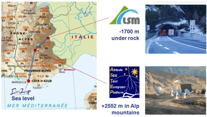
deploying the test in altitude (at least for neutrons, Figure 2). However, the acceleration factor AF (i.e. the ratio of the neutron integrated flux at the test location divided by its reference value at New-York City, NYC [12]) has nothing to do with those reached in accelerated tests. Considering an equivalence of the radiation background composition in altitude and at sea level [12], typical AF values between 5 and 20 as a function of the test location on Earth, can be expected. Devices have thus to be tested for a long enough period of time (months or years) until enough soft errors have been accumulated to give a reasonably confident estimate of the SER. The main advantage of RTSER tests is that they provide a direct measurement of the “true” SER that does not require intense radiation sources and extrapolations to use conditions. The major drawbacks of this method concern the cost of the system (which has to be capable of monitoring a very large number of devices at the same time) and the long duration of the experiment.
4.2. Soft error modelling
Modelling and simulating the effects of ionizing radiation has long been used for better understanding radiation effects on the operation of devices and circuits. In the last two decades, due to substantial progress in simulation codes and computer performances that reduce computation times, simulation has acquired significantly increased interest [17-18]. Due to its predictive capability, simulation offers the possibility to reduce radiation experiments and to test hypothetical devices or conditions, which are not feasible (or not easily measurable) by experiments. The continuous reduction of the feature size in microelectronics requires increasingly complicated and time-consuming manufacturing processes. Therefore, a systematic experimental investigation of the radiation effects of new ultra-scaled devices or emerging devices with alternative architecture (such as multiple-gate or silicon nanowire transistors) is difficult and expensive. Since computers are today considerably cheaper resources, simulation is becoming an indispensable tool for the device engineer, not only for the device optimization, but also for specific studies such as the device sensitivity when subjected to ionizing radiation. Last but not least, the understanding of the soft error mechanisms in ultra-scaled devices and the prediction of their occurrence under a given radiation environment are of fundamental importance for certain applications requiring a very high level of reliability and dependability [9].
5
. Radiation response of advanced technologiesWhile CMOS technologies continue to shrink in a "More Moore" perspective, new risks are arising with scaling for single event effects (SEE). Indeed, the SEE susceptibility of advanced technologies is expected to evolve under the influence of several factors since extrinsic radiation does not scale down. The most important are [19-20]: 1) the reduction of the critical charge, 2) the reduction of the per-bit cross-sections presented to ionizing particles, 3) the reduction of the energy-deposition volumes traversed by the particle at front-end level, 4) the increase of the particle region of influence at layout level and 5) the amplification of parasitic effects as a function of device architecture considered.
References
[1] P. E. Dodd and L. W. Massengill, Basic mechanisms and modeling of single- event upset in digital microelectronics, IEEE Trans. Nucl. Sci., vol. 50, no. 3, pp. 583–602, 2003.
[2] R.C. Baumann, Radiation-induced soft errors in advanced semiconductor technologies, IEEE Trans. Device Mater. Reliab., vol. 5, no. 3, pp. 305–316, 2005.
[3] J.L. Autran and D. Munteanu, Soft Errors: From Particles to Circuits, Taylor Francis/CRC Press, Boca Raton, FL, 2015.
[4] S. Mitra, P. Sanda, and N. Seifert, Soft errors: Technology trends, system effects and protection techniques, presented at IEEE International On-Line Testing Symposium (IOLTS), Crete, Greece, July 8– 11, 2007.
[5] R.D. Schrimpf and D.M. Fleetwood (Eds.), Radiation Effects and Soft Errors in Integrated Circuits and Electronic Devices, World Scientic Publishing, Singapore, 2004.
[6] E. Normand, Single event upset at ground level, IEEE Trans. Nucl. Sci., vol. NS-43, no. 6, pp. 2742–2750, 1996.
[7] E.H. Cannon, M. Cabanas-Holmen, J. Wert, T. Amort, R. Brees, J. Koehn, B. Meaker, and E. Normand, Heavy ion, high-energy, and low-energy proton SEE sensitivity of 90-nm RHBD SRAMs, IEEE Trans. Nucl. Sci., vol. 56, no. 7, pp. 3493–3499, 2010. [8] B.D. Sierawski, M.H. Mendenhall, R.A. Reed, M.A.
Clemens, R.A. Weller, R.D. Schrimpf, E.W. Blackmore, et al., Muon-induced single event upsets in deep-submicron technology, IEEE Trans. Nucl. Sci., vol. 57, no. 6, pp. 3273–3278, 2010.
[9] J.F. Ziegler and H. Puchner, SER – History, Trends and Challenges, Cypress Semiconductor, San Jose, CA, 2004.
[10] J.L. Autran, D. Munteanu, P. Roche, G. Gasiot, S. Martinie, S. Uznanski, S. Sauze, et al., Soft-errors induced by terrestrial neutrons and natural alpha- particle emitters in advanced memory circuits at ground level, Microelectron. Reliab., vol. 50, pp. 1822–1831, 2010.
[11] M. Glorieux, J.L. Autran, D. Munteanu, S. Clerc, G. Gasiot, and P. Roche, Random-walk drift-diffusion charge-collection model for reverse-biased junctions embedded in circuits, IEEE Trans. Nucl. Sci., vol. 61, pp. 3527–3532, 2014.
[12] JEDEC, Measurement and reporting of alpha particles and terrestrial cosmic ray-induced soft errors in semiconductor devices, JESD89, JEDEC Solid State Technology Association, Arlington, VA, 2006. [13] J.L. Autran, P. Roche, S. Sauze, G. Gasiot, D.
Munteanu, P. Loaiza, M. Zampaolo, and J. Borel,
Altitude and underground real-time SER
characterization of CMOS 65nm SRAM, IEEE Trans. Nucl. Sci., vol. 56, no. 4, pp. 2258–2266, 2009. [14] J.L. Autran, S. Serre, D. Munteanu, S. Martinie, S.
Semikh, S. Sauze, S. Uznanski, G. Gasiot, and P. Roche, Real-time soft-error testing of 40nm SRAMs, in 2012 IEEE International Reliability Physics Symposium, Anaheim, CA, April 15–19, 2012, pp. 3C.5.1–3C.5.8.
[15] J.L. Autran, D. Munteanu, G. Gasiot, and P. Roche, Real-time soft-error rate measurements: A review, Microelectron. Reliab., vol. 54, pp. 1455–1476, 2014. [16] J.L. Autran, D. Munteanu, S. Sauze, G. Gasiot, and P. Roche, Altitude and under- ground real-time SER testing of SRAMs manufactured in CMOS bulk 130, 65 and 40 nm, presented at 2014 IEEE Radiation Effects Data Workshop (REDW), Paris, July 14–18, 2014.
[17] P.E. Dodd, Physics-based simulation of single-event effects, IEEE Trans. Device Mater. Reliab., vol. 5, no. 3, pp. 343–357, 2005.
[18] D. Munteanu and J.L. Autran, Modeling and simulation of single-event effects in digital devices and ICs, IEEE Trans. Nucl. Sci., vol. 55, no. 4, pp. 1854–1878, 2008.
[19] P. Roche, J.L. Autran, G. Gasiot, and D. Munteanu, Technology downscaling worsening radiation effects in bulk: SOI to the rescue, in IEEE International Electron Device Meeting (IEDM), Washington, DC, December 9–11, 2013, pp. 766–769.
[20] L.W. Massengill, B.L. Bhuva, W.T. Holman, M.L. Alles, and T.D. Loveless, Technology scaling and soft error reliability, in 2012 IEEE International Reliability Physics Symposium (IRPS), Anaheim, CA, April 15– 19, 2012, pp. 3C.1.1–3C.1.7.
Figure 1. Mechanisms of Soft Errors: particle Monte Carlo Simulation (RWDD model – IM2NP).