Publisher’s version / Version de l'éditeur:
Vous avez des questions? Nous pouvons vous aider. Pour communiquer directement avec un auteur, consultez la première page de la revue dans laquelle son article a été publié afin de trouver ses coordonnées. Si vous n’arrivez pas à les repérer, communiquez avec nous à [email protected].
Questions? Contact the NRC Publications Archive team at
[email protected]. If you wish to email the authors directly, please see the first page of the publication for their contact information.
https://publications-cnrc.canada.ca/fra/droits
L’accès à ce site Web et l’utilisation de son contenu sont assujettis aux conditions présentées dans le site LISEZ CES CONDITIONS ATTENTIVEMENT AVANT D’UTILISER CE SITE WEB.
Journal of Applied Physics, 104, 2008-08
READ THESE TERMS AND CONDITIONS CAREFULLY BEFORE USING THIS WEBSITE. https://nrc-publications.canada.ca/eng/copyright
NRC Publications Archive Record / Notice des Archives des publications du CNRC :
https://nrc-publications.canada.ca/eng/view/object/?id=c69c4548-187c-4d9c-a561-0427c43786cf
https://publications-cnrc.canada.ca/fra/voir/objet/?id=c69c4548-187c-4d9c-a561-0427c43786cf
NRC Publications Archive
Archives des publications du CNRC
This publication could be one of several versions: author’s original, accepted manuscript or the publisher’s version. / La version de cette publication peut être l’une des suivantes : la version prépublication de l’auteur, la version acceptée du manuscrit ou la version de l’éditeur.
For the publisher’s version, please access the DOI link below./ Pour consulter la version de l’éditeur, utilisez le lien DOI ci-dessous.
https://doi.org/10.1063/1.2970093
Access and use of this website and the material on it are subject to the Terms and Conditions set forth at
Vacancy-mediated intermixing in InAs/InP(001) quantum dots subjected
to ion implantation
Dion, C.; Desjardins, P.; Schiettekatte, F.; Chicoine, M.; Robertson, M. D.;
Shtinkov, N.; Poole, P. J.; Wu, X.; Raymond, S.
Vacancy-mediated intermixing in InAs/InP„001… quantum dots
subjected to ion implantation
C. Dion,1,a兲P. Desjardins,1F. Schiettekatte,2M. Chicoine,2M. D. Robertson,3
N. Shtinkov,4P. J. Poole,5X. Wu,5and S. Raymond5
1
Regroupement Québécois sur les Matériaux de Pointe (RQMP), Département de Génie Physique, École Polytechnique de Montréal, Montréal, Québec H3C 3A7, Canada
2
Regroupement Québécois sur les Matériaux de Pointe (RQMP), Département de Physique, Université de Montréal, Montréal, Québec H3C 3J7, Canada
3
Department of Physics, Acadia University, Wolfville, Nova Scotia B4P 2R6, Canada
4
Department of Physics, University of Ottawa, Ottawa, Ontario K1N 6N5, Canada
5
Institute for Microstructural Sciences, National Research Council, Ottawa, Ontario K1A 0R6, Canada
共Received 30 April 2008; accepted 18 June 2008; published online 28 August 2008兲
We have investigated the influence of defects emanating from phosphorus implantation damage in the InP capping layer on postgrowth thermally induced intermixing in self-assembled InAs/InP共001兲
quantum dots共QDs兲. Photoluminescence 共PL兲 spectra from as-grown samples could be described as
the superposition of separate PL peaks where each peak corresponded to emission from an ensemble of QDs with a particular height ranging from 4 to 13 ML. Blueshift of up to 270 meV and significant bandwidth broadening were observed in the PL spectra after ion implantation with a fluence of 5 ⫻ 1011− 1014 cm−2and subsequent annealing at temperatures ranging from 450 to 600 ° C. From the analysis of the evolution of the QD peaks upon intermixing, which revealed the coexistence of intact QD PL and a broad PL feature related to heavily intermixed QDs, it was suggested that the bandwidth broadening resulted from spatial inhomogeneity in the compositional intermixing. In order to better understand the mechanism responsible for the ion-implantation-induced intermixing, samples capped with a stack of compressively strained In0.75Ga0.25As/ InP quantum wells 共QWs兲 were prepared to trap vacancies released by the implantation damage while not inhibiting the effect of the interstitials. Both blueshift and bandwidth broadening were suppressed in samples containing the strained InGaAs QWs, whereas the evolution of the PL spectra from the QDs behaves as expected for interstitial-mediated intermixing. The vacancies were thus believed to be trapped in the QWs and indicated that intermixing in ion-implanted InP capped samples is mediated by vacancies. The shape of the QDs changed from a truncated pyramid in the as-grown state to a double convex lens structure after intermixing as confirmed by cross-sectional scanning transmission electron microscopy imaging. Furthermore, the change in shape and compositional intermixing of the QDs were attributed to vacancy trapping in the vicinity of the QDs as based on atomistic strain calculations. © 2008 American Institute of Physics.关DOI:10.1063/1.2970093兴
I. INTRODUCTION
Considerable attention has been given to self-assembled
InAs/InP quantum dots共QDs兲 as active elements in tunable
lasers for use in the next generation of optical networks and
biological imaging systems operating in the 1.5 m
wave-length range.1–3 The integration of QDs into modern opto-electronic devices is dependent on being able to precisely control their emission wavelength which can be achieved by postgrowth band gap tuning via thermally induced interdif-fusion of atoms at the QD/barrier interface. This modifies the confinement potential and hence the energy levels of the heterostructure. The compositional intermixing process is fa-cilitated by the motion of point defects that are either native or intentionally incorporated into specific regions of the sample, for example, by low temperature growth of the
cap-ping layer 关grown-in defects 共GID兲兴,4dielectric capping,5or high-energy共low-energy兲 ion implantation above6共through7兲 the emitting layer.
In ion-implanted heterostructures, both interstitial- and vacancy-mediated processes can stimulate compositional in-termixing. Given that the evolution of the photolumines-cence共PL兲 characteristics with annealing time and tempera-ture is similar for dielectric capping, GID, and low-energy
ion implantation 共LEII兲, it was assumed by several authors
that the dominant defects responsible for intermixing in InGaAs/InP quantum wells 共QWs兲 were P interstitials.4,8 In
InAs/InP QDs, intermixing using conventional annealing,9
laser annealing,10 dielectric capping,10–12 and GID13 gener-ally resulted in a progressive blueshift of the overall QD emission spectra with no significant peak broadening. In sharp contrast, intermixing stimulated by the creation of de-fects in the capping layer using ion implantation yielded sig-nificant bandwidth broadening of the emission spectra.14,15 Furthermore, the temperature threshold required to induce intermixing in ion-implanted samples was significantly
re-a兲
Author to whom correspondence should be addressed. Also at the Institute for Microstructural Sciences, National Research Council, Ottawa, Ontario K1A 0R6, Canada. Electronic mail: [email protected].
JOURNAL OF APPLIED PHYSICS 104, 043527共2008兲
duced共⬃400 ° C兲 as compared to the other techniques
men-tioned above 共⬃600– 725 ° C range兲. These latter results
suggest that the dominant defect responsible for intermixing in ion-implanted InAs/InP QDs is different than P intersti-tials, possibly vacancies which are also created as a result of the ion-implantation damage.
In this work, we used PL spectroscopy and
cross-sectional scanning transmission electron microscopy
共STEM兲 to investigate ion-implantation-induced intermixing in InAs/InP QDs. Two series of experiments were performed to elucidate the underlying mechanism. In the first set of experiments, the influence of the annealing temperature, the distance between implantation damage in the InP capping layer and the InAs QDs, and the P implantation fluence on QD PL characteristics was examined. It is shown that the ion-implantation-induced intermixing process is spatially in-homogeneous and characterized by the presence of relatively intact as well as extensively intermixed areas. In order to discriminate the effects of interstitials and vacancies on the intermixing dynamics, a second set of experiments was per-formed on samples capped with compressively strained InGaAs/InP QWs which were known to trap vacancies ema-nating from the implanted region.16,17From these results, we show that intermixing in ion-implanted InP capped InAs/InP QDs is dominated by the motion of vacancies. In addition, as confirmed using STEM imaging and atomic strain calcula-tions, vacancy trapping also occurs in the compressively strained InAs/InP QDs, which is believed to be the main mechanism responsible for the ion-implantation-induced in-termixing observed at a relatively low temperature anneal-ing.
II. EXPERIMENTAL DETAILS
All samples were grown on semi-insulating Fe-doped InP共001兲 substrates by chemical beam epitaxy from trimeth-ylindium, arsine, and phosphine. The sample used for ion-implantation-induced intermixing experiments consisted of a
128 nm thick InP buffer layer,⬃2.2 ML of InAs, followed
by a 25 s growth interruption, and a 30 nm thick InP capping layer, all grown at 515 ° C. The temperature was then ramped down to 500 ° C for the growth of a 790 nm thick InP layer. We have also examined intermixing in a sample containing GID.13,18This sample consisted of a 120 nm thick
InP buffer layer, ⬃2.2 ML of InAs, followed by a 35 s
growth interruption to allow QD formation, and a 40 nm thick InP capping layer, all grown at 505 ° C. The tempera-ture was then ramped down to 450 ° C for the growth of a 760 nm thick InP layer which contained a large quantity of GID as compared to samples grown at the standard
tempera-ture of⬃500 ° C. Optimal growth conditions were then used
for the growth of a 33 nm thick InGaAs capping layer. More precisely, GID in low temperature grown InP are related to a P-rich stoichiometry with a large quantity of PIn antisite defects,19,20 which upon annealing result in an excess of P interstitials that promote interdiffusion.21,22
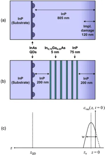
The samples used for the experiments on vacancy trap-ping in compressively strained QWs are shown
schemati-cally in Figs. 1共a兲 and 1共b兲. The sample represented in
Fig. 1共a兲 consisted of a 125 nm thick InP buffer layer,
⬃2.9 ML InAs QD layer, followed by a 25 s growth inter-ruption, and a 32 nm thick InP capping layer, all grown at 515 ° C. The temperature was then ramped down to 500 ° C for the growth of a 773 nm thick InP layer so that the total InP capping layer thickness was 805 nm. The sample shown in Fig.1共b兲was similar to that just described, except that a six period stack of 5 nm thick In0.75Ga0.25As QWs with 75 nm InP spacers was inserted in the InP capping layer, 200 nm away from both the surface and the QD plane. The indium concentration and QW thickness were chosen to produce 1.5% of compressive strain while avoiding the creation of dislocations in the heterostructure.23
Samples were implanted with phosphorus ions to avoid introducing additional chemical impurities. Implantations
were performed at 7° off the 共001兲 direction to minimize
channeling effects. The substrate temperature was main-tained at 200 ° C to prevent surface amorphization6 and the implantation fluence ⌽ ranged from 5 ⫻ 1011 to 1014 cm−2. Based onSRIM 2000simulations,24 the energy of P ions was set to 30 keV to confine implantation damage to the first
120 nm below the top surface 关see Fig. 1共c兲兴. In order to
examine the influence of the distance between the implanted region and the InAs QDs on the intermixing dynamics,
FIG. 1. 共Color online兲 Schematic illustrations of the 共a兲 InP and 共b兲 QW-capped samples, and共c兲 initial defect concentration profile, cvac共z , t = 0兲, as a
function of position z, zQDand z0are respectively the QD position and the
pieces of the sample containing compressively strained InGaAs/InP QWs were chemically etched before ion implan-tation so that only 200 nm of InP remained on top of the QD
layer. The InGaAs QWs were removed using a
C6H8O7: H2O2 共3:1兲 solution, while a HCl: H3PO4 共1:3兲 so-lution was used for the etching of the InP.
Samples were subjected to rapid thermal annealing 共RTA兲 using an AG Associates Heatpulse 410 system in a VLSI grade nitrogen atmosphere. In order to prevent exces-sive loss of group V atoms during annealing, all samples were proximity capped with InP substrates, except for the GID samples which were covered with GaAs. The thermal
annealing was performed at temperatures Ta in the
450– 750 ° C range for times ta of either 120 or 300 s.
Low temperature 共77 K兲 PL measurements were
con-ducted using the 532 nm line of a Nd: YVO4 laser as the
excitation source, except for the GID samples which were probed using the 760 nm line of a Ti:sapphire so that the InGaAs capping layer could be penetrated. In both cases, the incident light power density was kept constant at 50 W cm−2
over a 50 m diameter beam spot that probed
approxi-mately 105 QDs. The spectra were acquired using a double
grating spectrometer and a liquid nitrogen cooled germanium detector. The resolution of the acquisition system was about 4 meV. In order to properly observe the QD emission in the samples containing the InGaAs QWs, the QWs were etched away prior to PL measurement. While the as-grown struc-tures were etched using the solutions described above, inter-mixed InGaAsP QWs had to be removed using a H2SO4: H2O2: H2O共1:1:10兲 solution due to the highly selec-tive nature of the C6H8O7: H2O2 共3:1兲 solution used for In-GaAs etching.
Structural investigations of the samples were performed using cross-sectional high-angle annular dark field STEM 共HAADF-STEM兲. The samples were prepared by low-angle
polishing using an Allied High Tech Products Inc.
MultiPrep™ system, followed by low-angle argon ion mill-ing usmill-ing a Fischione model 1010 ion mill. Details of the specimen preparation have been previously published.25,26 HAADF-STEM imaging was performed at 200 kV using a JEOL JEM-2100 F STEM equipped with a Gatan ADF
de-tector 共5–11 mm active diameter兲. The inner detector angle
of the ADF detector was set to 51 mrad.
III. EXPERIMENTAL RESULTS
A. Ion-implantation-induced intermixing
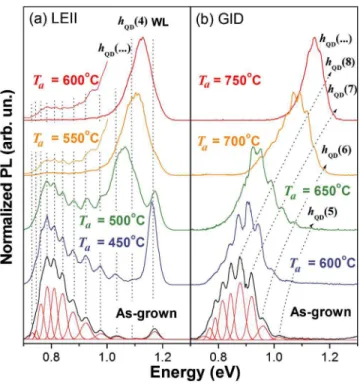
PL spectra from as-grown and intermixed InAs/InP QDs subjected to P implantation共⌽ = 1014 cm−2兲 and annealing at various temperatures are presented in Fig. 2共a兲. In order to better highlight the specific effects of ion-implantation-induced intermixing, the PL spectra are compared to those
obtained for GID-mediated intermixing 关see Fig. 2共b兲兴. In
both sets of experiments, the as-grown samples are charac-terized by a broad emission, centered near 850 meV, arising from the superposition of up to ten inhomogeneously broad-ened peaks. These peaks correspond to the fundamental
electron⫺heavy-hole transitions 共e1-hh1兲 of ensembles, or
families, of QDs each having the same thickness 共hQD兲 in
terms of an integer number of monolayers.27,28 The
low-intensity peak observed at 1160 meV in Fig. 2共a兲 can be
attributed to the emission from the wetting layer共WL兲.29The relative intensities of the QD peaks and the WL are indica-tors of the island thickness distribution and QD density, which can vary slightly from one sample to another depend-ing on the growth conditions.30For instance, the appearance of a WL peak in the GID sample can probably be attributed to a lower density of QDs.30As discussed in Ref.28, tight-binding calculations were combined with PL results in order to determine the height and P concentration of each QD fam-ily in their as-grown state. We have found that the optical transitions from both as-grown LEII and GID samples
pre-sented in Fig. 2 arise from 5 to 13 ML thick QDs with an
average P composition of 关P兴 = 9.3⫾ 0.7%. This indicates
that both samples are structurally similar, a necessary condi-tion for comparison of their properties after different inter-mixing treatments.
Despite their similarities in the as-grown state, the LEII and GID samples display very different PL behavior after
annealing. As shown in Fig. 2共b兲, the overall QD emission
spectra from the GID samples exhibit a progressive blueshift without bandwidth broadening. No significant change in the
overall peak shape and width is observed for Ta of up to
700 ° C. After annealing at 750 ° C, the maximum intensity
of the PL spectrum is located at⬃1.1 eV and the peak
be-comes narrower with less resolved subpeaks. This results suggest that the thinner QDs progressively dissolve into the
FIG. 2. 共Color online兲 共a兲 PL spectra at 77 K from as-grown and annealed LEII samples with a fluence of ⌽ = 1014 cm−2 as a function of T
a for
ta= 300 s.共b兲 PL spectra at 77 K from as-grown and annealed GID samples
as a function of temperature Tafor time ta= 300 s. A typical example of the
peak fitting operation is illustrated for the as-grown samples. Dashed lines illustrate the evolution of the various QD emission peaks, where the numeral in hQD共i兲 refers to the QD ensemble thickness in terms of an integer number
of monolayers. Fine lines in共a兲 are magnifications of the spectra in that energy range.
WL to form a highly disordered QW.13In contrast, as shown in Fig. 2共a兲, no progressive blueshift of the PL spectra is observed from LEII samples upon annealing; however, at comparatively much lower annealing temperatures, a high-energy peak emerges over the original QD emission spec-trum. In addition, substantial bandwidth broadening of the PL spectra is observed. After annealing at 600 ° C, the PL spectrum becomes dominated by a wide emission peak lo-cated at⬃1.1 eV that can be attributed to the emission from heavily intermixed QDs. The sudden rise of this high-energy peak, without going through intermediate energy values, sug-gests that QDs experienced significant and rapid composi-tional interdiffusion.14
In order to quantify the evolution of the PL spectra due to intermixing, all spectra presented in Fig.2were analyzed using a multiparameter fit assuming a single Gaussian curve per QD family peak. As a starting point, the initial peak positions for the as-grown samples were estimated based on
a previous work.28 The full widths at half maximum
共FWHM兲 of the peaks—which are related to inhomogeneous broadening within a given family due to small variations in lateral size, composition, electronic environment, or from roughness in the thickness27—were constrained to increase with emission energy since interfacial roughness is expected to cause larger relative changes in the confinement emission energy in thinner QDs.31The results of this fitting procedure are illustrated in Figs. 2共a兲and 2共b兲 for the as-grown state where the peaks are labeled in terms of hQD. The peak ener-gies obtained for the as-grown samples were then used to initialize the fit of the spectra from annealed samples. In order to quantify the progressive blueshift of individual QD family peaks in the GID samples关Fig.2共b兲兴, a uniform shift was first applied to all as-grown transition energies and indi-vidual peak positions and FWHM were then fit to obtain the best match to each spectrum. For the LEII samples, no pro-gressive blueshift of the QD peaks is observed upon anneal-ing in Fig. 2共a兲. In this case, the evolution of PL spectra is explained by changes in the relative intensities of the indi-vidual peaks. Indeed, as indicated by the dotted line in Fig.2共a兲, the QD peaks appear to remain at their initial en-ergies. A significant reduction in the PL intensity of the low-energy peaks associated with thicker QDs is accompanied by the sudden rise of a broad high-energy PL peak with energy corresponding to that of thinner QDs and heavily intermixed QDs. In such samples, the best fits were obtained by keeping the QD peak position energies constant while allowing varia-tions in their amplitude and FWHM. The fitting procedures for the LEII and GID samples were not interchangeable since some QD peaks from the annealed GID samples were found to be located at intermediate energy values, between the two as-grown states. Similarly, it was not possible to attribute the sudden rise of the high-energy peak in PL spectra from an-nealed LEII samples to a progressive energy shift. In all cases, the fitting procedure allows the determination of the peak energy and FHWM within ⫾5 meV.
The results of the fitting procedure共peak position and
FWHM of each QD peak兲 are presented in Figs. 3共a兲 and
3共b兲for the GID samples. In Fig.3共a兲, the peaks attributed to different QD ensembles shift at similar rates with annealing,
as observed in previous publications.13,18 No evidence of
peak broadening with annealing can be seen in Fig. 3共b兲
where the FWHM remains comparable, within uncertainty, to that in the as-grown state. Consequently, the combination of similar energy shifts and fairly constant FWHM for all QD ensembles results in a relatively constant overall emis-sion bandwidth upon intermixing. Hence, all QDs underwent a similar degree of intermixing, meaning that intermixing in the GID samples was relatively spatially uniform.
The amplitude and FWHM of each peak in the PL spec-tra are presented in Figs. 3共c兲and3共d兲as a function of
an-nealing temperature for LEII samples. The amplitude 关Fig.
3共c兲兴 of the emission peaks attributed to QD ensembles with 4, 5, and 6 ML in thickness increase by up to two orders of magnitude after annealing. Since the sudden appearance of a higher density of small QDs is physically unlikely and that the energies associated with heavily intermixed structures of all size in the 0.95–1.15 eV range are similar to those for 4⫺6 ML thick as-grown QDs, an increase in the population of heavily intermixed structures is believed to have occurred. In addition, the FWHM of these peaks increase from 40 meV in the as-grown state to 80 meV after annealing at 600 ° C. This is consistent with the fact that emission in that energy range arises from a heavily disordered system composed of QDs of different sizes and compositions. On the other hand, the emission peaks from QD ensembles of more than 7 ML decrease in amplitude by one order of magnitude, while their FWHM remains constant. This indicates that these emission peaks arise from intact QDs, where many of the QDs previ-ously emitting of this region of the spectrum have now heavily intermixed and contribute to the emission of the broad spectral feature in the region of 0.95⫺1.15 eV.
FIG. 3.共Color online兲 Evolution of the QD emission peaks as a function of annealing temperature Ta. In共a兲 and 共b兲 are the evolution of the peak
posi-tion and FWHM, respectively, for GID samples. In共c兲 and 共d兲 are presented the evolution of the peak amplitude and FWHM, respectively, for LEII samples. The symbols correspond to the various QD ensembles with differ-ing thickness.
Altogether, the above results demonstrate that the PL spectra originate from a superposition of multiple emission peaks from both as-grown and heavily intermixed structures. The coexistence of nonintermixed and heavily intermixed QDs
within the probed region 共about 50 m in diameter兲
sug-gests that intermixing is spatially nonuniform throughout the sample.
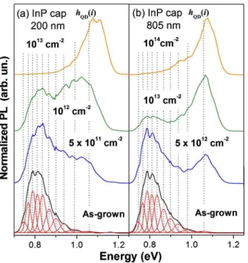
The peculiar PL progression with annealing temperature observed in Fig.2共a兲is a general behavior in all of the LEII samples investigated, independent of the P implantation flu-ence and of the distance between the implanted zone and the InAs QDs. This effect is illustrated in the PL spectra
ob-tained from samples capped with共a兲 200 nm and 共b兲 805 nm
thick InP as a function of implantation fluence for
Ta= 575 ° C, as shown in Fig. 4. Similar to the PL spectra
shown Fig.2, ion-implantation-induced intermixing leads to a reduction in the relative intensity of the low-energy peaks associated with thicker QDs together with an increase in the relative intensity of the high-energy peaks attributed to the thinner and heavily intermixed QDs. This leads to an appar-ent overall blueshift with significant bandwidth broadening. Comparing the results between the samples with 200 and 805 nm InP caps reveals that the ion fluences required to achieve similar PL characteristics differ by about one order of mag-nitude. As will be discussed in Sec. IV, this important result provides insights into the transport dynamics of defects, from their creation location in the InP capping layer to the active InAs QD region.
The results presented in Figs.2共a兲and4, together with
other published data 共see, for example, Refs. 14 and 15兲,
indicate that the observed overall PL evolution is common to all ion-implanted InAs/InP QDs even though the changes in the relative intensities between the low- and high-energy peaks are a strong function of annealing and implantation conditions. This behavior is significantly different from that obtained using other intermixing techniques such as GID as shown in Fig. 2共b兲. Since the motion of P interstitials had
been previously proposed to explain GID-induced
intermixing,13 it is reasonable to formulate the hypothesis that the ion-implantation-induced intermixing originates from the presence of vacancies which were also released from the implanted region of the sample.
B. Vacancy trapping in compressively strained InGaAs/InP QWs
The samples shown schematically in Figs.1共a兲and1共b兲
were used to discriminate the effects of vacancies and
inter-stitials on intermixing. In Fig. 1共b兲, the compressively
strained InGaAs/InP QWs were used to trap vacancies while not inhibiting the effects of the interstitials.16,17 Indeed, in a system containing a nonuniform stress field, diffusing par-ticles experience a force in the direction that reduces their interaction energy with the stress field.32,33As vacancies in a host crystal create local tensile stresses, the system favors the propagation of these defects toward the compressively strained regions of the sample. Furthermore, because it re-quires more energy for vacancies to return to the lattice matched regions, these defects are likely to be trapped within the compressively strained layers.16On the other hand, inter-stitials cause local compressive stresses and hence these de-fects will diffuse away from the compressively strained regions.16
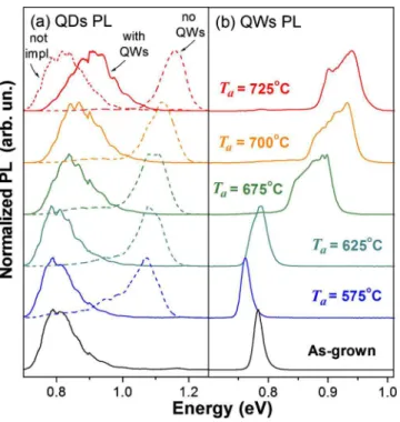
The evolution of the QDs PL characteristics from samples with and without the compressively strained
InGaAs/InP QWs after implantation with 1014 P cm−2 and
120 s anneals at Ta ranging from 575 to 725 ° C are
com-pared in Fig. 5共a兲. Implanted InP capped samples are char-acterized by pronounced intermixing as the QD emission evolves to essentially become a high-energy peak centered at about 1.1 eV, similar to the results presented in Figs.2共a兲and
4. In sharp contrast, the PL spectra from the sample compris-ing the strained QWs exhibit a slower progressive blueshift of up to 110 meV after annealing at 725 ° C with no cant change in the overall peak shape and width. No signifi-cant blueshift was measured in an unimplanted reference sample annealed under the same conditions, as highlighted by the dotted spectra in Fig. 5共a兲.
Comparing the results in Fig.5共a兲with those in Fig.2共b兲
reveals that the PL evolution from implanted and annealed QW-capped samples is similar to that observed in samples containing GID, in which intermixing is known to be medi-ated by the motion of interstitials.4,13Since drastic intermix-ing is suppressed in the presence of the compressive QWs, we attribute the origin of the significant and peculiar inter-mixing observed in implanted and annealed InP capped samples to the motion of vacancies created by the ion-induced damage.
As mentioned in Sec. II, the QD PL spectra presented in Fig.5共a兲from samples capped with a stack of compressively
FIG. 4. 共Color online兲 PL spectra at 77 K from intermixed QD samples capped with共a兲 200 nm and 共b兲 805 nm thick InP as a function of implan-tation fluence ⌽ for annealing temperature Ta= 575 ° C and time ta
= 120 ° C. PL spectra at 77 K from as-grown QDs are also shown for com-parison. Results of the peak fitting operation are illustrated for as-grown samples. Dashed vertical lines indicate the peak position of the various QD ensembles.
strained QWs were obtained after carefully etching away the QWs after ion implantation and annealing in order to elimi-nate emission from the QWs. Nevertheless, the QW emission characteristics from unetched samples presented in Fig.5共b兲
provide insights into the intermixing dynamics within the strained QW stack. Spectra from as-grown InGaAs QWs are characterized by a single emission peak centered at around 780 meV corresponding to the e1-hh1 transition.34Although not explicitly shown here, QW PL peaks from unimplanted
samples experience no significant shift for Ta below
750 ° C.35,36 On the other hand, QW PL spectra from
im-planted and annealed samples exhibit a redshift of about 20 meV after 120 s anneals at Ta below 575 ° C and a
blue-shift up to about 160 meV for Ta= 725 ° C. Similar PL
char-acteristics were observed by Nie et al.37 from InGaAsP/InP QWs subjected to ion implantation by plasma immersion and
RTA. These authors, together with Micallef et al.,38 have
shown theoretically that both red- and blueshifts can be at-tributed to interdiffusion at the InGaAsP/InP interfaces with the sign of the emission shift depending upon the predomi-nance of either group III 共redshift兲 or group V 共blueshift兲 atomic interdiffusion. In addition, the PL spectra displayed in Fig.5共b兲show significant bandwidth broadening, suggesting that the numerous QWs undergo different degrees of inter-mixing. This observation is consistent with the fact that de-fects promoting intermixing are emanating from the im-planted region on the top surface and that their concentration decreases for QWs located deeper into the structure. This is also in agreement with vacancy trapping in the
compres-sively strained QWs as the structures located nearer to the surface can be expected to trap the largest number of vacan-cies.
As PL results are only indirect evidence of intermixing, STEM investigations were used to confirm that various QWs exhibit progressively decreasing degrees of intermixing as vacancy diffusion progresses deeper into the sample. A typi-cal cross-sectional image of the entire QW stack is shown in Fig.6共a兲while Figs.6共b兲and6共c兲are higher magnification images of the first QW 共relative to the top surface兲 in the
as-grown state and after intermixing 共⌽ = 1014 cm−2, T
a
= 725 ° C, and ta= 120 s兲. Line scan profiles of the image
intensity from every QW after intermixing, averaged over five measurements from different locations in the high
mag-FIG. 5.共Color online兲 共a兲 PL spectra at 77 K from as-grown and intermixed 共⌽ = 1014 cm−2; T
a= 575– 725 ° C, ta= 120 s兲 QDs in samples capped with
pure InP 共dashed lines兲 and a stack of compressively strained In0.75Ga0.25As/ InP QWs共solid lines兲. PL spectrum at 77 K from an
unim-planted InP capped sample 共dotted line兲 annealed at Ta= 725 ° C for ta
= 120 s is also shown for comparison.共b兲 PL spectra at 77 K from as-grown and intermixed共⌽ = 1014 cm−2; T
a= 575– 725 ° C, ta= 120 s兲 In0.75Ga0.25As
QWs prior to wet chemical etching.
FIG. 6. 共Color online兲 共a兲 Cross-sectional HAADF-STEM images of the as-grown QW stack. Higher magnification images of the first QW relative to the surface共b兲 prior to treatment and 共c兲 after intermixing 共⌽ = 1014 cm−2; Ta= 725 ° C, ta= 120 s兲. 共d兲 Line scan profiles across the intermixed QWs
共⌽ = 1014 cm−2; T
a= 725 ° C, ta= 120 s兲. A typical profile of an as-grown
nification images, are presented in Fig. 6共d兲. In addition, a typical profile from an as-grown QW is shown for compari-son. The degree of compositional intermixing is largest for QW closer to the surface, thereby corroborating the PL re-sults which showed that the QWs undergo different degrees of intermixing based on their location.
In summary, through the use of a specially designed structure containing compressively strained InGaAs QWs in the InP capping layer to trap vacancies, we have demon-strated that vacancies are the main agent driving composi-tional intermixing in ion-implanted InP capped InAs/InP QDs. This conclusion has major consequences on the under-standing of vacancy-mediated intermixing within InAs/InP QDs. Indeed, since InAs/InP QDs are compressively strained structures, they should also attract vacancies into their vicin-ity. This latter point is addressed in Sec. III C.
C. Vacancy trapping in compressively strained InAs/InP QDs
In order to examine the possibility of vacancy trapping in compressively strained InAs/InP QD structures, we have investigated the evolution of QD shapes with the degree of intermixing using STEM. The results for the LEII and GID samples were compared to highlight the specific effects of ion-implantation-induced intermixing. Samples exhibiting maximum and intermediate changes in PL in Fig.2, i.e., GID samples annealed at Ta= 750 and 600 ° C for ta= 300 s, and
LEII samples with fluence ⌽ = 1014 cm−2 annealed at
Ta= 600 and 500 ° C for ta= 300 s, were selected for these
measurements. Typical QD shapes for the various processing conditions are presented in Fig.7 for共a兲 as-grown, 关共b兲 and 共c兲兴 annealed GID, and 关共d兲 and 共e兲兴 annealed LEII samples.
The as-grown InAs/InP QDs 关Fig.7共a兲兴 are truncated
pyra-mids with flat top and bottom surfaces and 25° side angles,
corresponding to 共113兲 facets, in agreement with previous
reports.26,39,40Substantial modifications in the QD shape are observed in samples showing intermediate PL changes. For interstitial-mediated intermixing in GID samples the flat top becomes spherical, transforming the truncated pyramid QD into a domelike structure as shown in Fig.7共b兲. On the other hand, vacancy induced intermixing in the LEII samples alters both the top and bottom QD interfaces, creating a double convex lens as displayed in Fig.7共d兲. Although the diameter and the thickness of the QDs varied significantly for obser-vations made in different regions of the samples, these gen-eral QD shapes were consistently observed. Finally, for
samples showing maximum PL changes, Figs. 7共c兲and7共e兲
show broadened QWs, confirming the dissolution of a vast number of QDs into the WL. No distinct QD structures were found in these samples. This is consistent with the PL results displayed in Figs.2共a兲and2共b兲where both samples are char-acterized by a much broadened PL peak centered at around 1.1 eV.
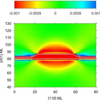
Although interstitials and vacancies both lead to broad-ened QW after significant intermixing, the nature of the de-fects promoting interdiffusion greatly afde-fects the QD shape in their intermediate intermixed states. Since strain affects the diffusion dynamics of the defects, we have examined this point in more detail using atomistic strain simulations similar to those presented in Ref.40 using Keating’s valence force field method41 with the parameters reported by Martins and Zunger.42The calculated hydrostatic strain distribution in the 关001兴 plane of a 6 ML thick pure InAs truncated pyramid
with 共113兲 side facets on a 2 ML thick InAs WL buried in
pure InP matrix is presented in Fig.8. The strain, expressed as a percentage, has been associated to a color scale, where
FIG. 7. 共a兲 Cross-sectional HAADF-STEM images 共关110兴 zone axis兲 of a typical as-grown QD. Images of typical structures in GID samples after annealing for ta= 300 s at共b兲 Ta= 600 ° C and共c兲 Ta= 750 ° C. Images of
typical structures in LEII samples with a fluence of ⌽ = 1014 cm−2after
annealing for ta= 300 s at共d兲 Ta= 500 ° C and共e兲 Ta= 600 ° C.
FIG. 8.共Color online兲 Calculated hydrostatic strain distribution in the 关001兴 plane of a 6 ML thick pure InAs truncated pyramid with共113兲 side facets on a 2 ML thick InAs WL buried in pure InP matrix. In the color scale, red and blue correspond to compressive and tensile strains, respectively.
negative共compressive兲 and positive 共tensile兲 strains refer to red and blue, respectively. The scale limits were fixed to −0.1% and 0.1% to clearly illustrate small strain variations in the InP matrix. In the scale range displayed, the strain distri-bution within the QD and WL appears homogeneous, al-though the actual strain values varied slightly between −3.3% and −2.9%. There is a significant level of compres-sive strain in the surrounding InP barrier material at the bot-tom and the top of the pyramidal island. Strain values in these regions are on the order of −0.1% and the compressive strain values gradually diminish away from the QD structure. In contrast, regions around the periphery of the island are under tensile strain up to 0.3%, which quickly decrease away from the QD structure. Similar strain distributions were re-ported in the literature for InAs QDs embedded in GaAs matrix.43,44
Defects traveling down from the top surface of the sample are subjected to the compressive and tensile strain fields around the QD. While interstitials are favorably di-rected toward the island periphery, the migration of vacan-cies toward the QDs is energetically favored. Thus, in interstitial-mediated intermixing, QD interdiffusion is ex-pected to proceed mostly along the side interfaces, producing graded QD edges. This is consistent with STEM images from the GID sample displayed in Fig.7共b兲. On the other hand, in vacancy-mediated intermixing, the compressive strain accu-mulation around the base and top surface of the QD should confine the mobile vacancies promoting interdiffusion in these regions. This is in good agreement with the double convex lens shape of QDs after ion-implantation-induced in-termixing presented in Fig.7共d兲.
The nature of the defects driving interdiffusion in InAs/ InP QDs does not only influence the evolution of the QD shape upon intermixing but also has an impact on the inter-diffusion dynamics. Since vacancies are confined in the vi-cinity of the QDs, a single vacancy is expected to induce numerous P–As substitutions at the InAs/InP heterojunction and should therefore produce significantly more intermixing than a single interstitial which is rapidly ejected away from the strained region.16 Consequently, the P–As substitution coefficient at a given Tais expected to be much larger when
it is promoted by vacancies than when it is controlled by the motion of interstitials. This is consistent with the lower Ta
threshold for intermixing observed in Fig. 2. In addition, since a small number of vacancies are required to produce a large level of interdiffusion, this process should be strongly influenced by the probability of the presence of a single va-cancy in a single QD. Therefore, it is expected that there will be a coexistence of both intact and intermixed QDs within the sample, which is consistent with the spatial inhomogene-ity of ion-implantation-induced intermixing as observed in Sec. III A.
IV. DISCUSSION
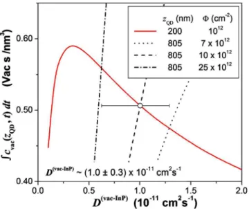
In order to gain further insight into the dynamics of va-cancy diffusion, we have conducted a quantitative analysis of the results displayed in Fig.4which highlights InAs/InP QD samples with 200 and 805 nm thick InP capping layers with
comparable PL characteristics for implantation fluences dif-fering by about one order of magnitude. Based on these ob-servations, we may assume that both experimental conditions led to comparable intermixing diffusion lengths. Further-more, assuming that atomic interdiffusion in the vicinity of the QDs was governed by a sole diffusion species— vacancies based on the results presented in Sec. III B—the diffusion length of intermixing LI after a given annealing
time ta can be written as
4,33,45 LI2=4D 共P–As兲 n0
冕
0 ta cvac共zQD,t兲dt, 共1兲where D共P–As兲 is the P–As substitution coefficient at the QD boundary and cvac共zQD, t兲 / n0 is the concentration of
vacan-cies at the QD position zQD as a function of time t with
respect to the total concentration of vacancy sites available
n0. Since both samples were subjected to 120 s anneals at a temperature of 575 ° C, it can be reasonably assumed that values of D共P–As兲 are the same in both conditions. This as-sumption is valid provided that D共P–As兲 is not concentration
dependent, a reasonable hypothesis for InAs/InP QDs.18
Thus, based on Eq. 共1兲, both experimental conditions must
lead to the same time-integrated cvac共zQD, t兲 value.
Since the concentration of P vacancies共VP兲 released by the ion-induced damage is believed to be much larger that the concentration of native defects in thermal equilibrium, vacancies are expected to dominate intermixing dynamics. Under these assumptions, we can estimate the diffusion co-efficient associated with the transport of vacancies from their creation location in the InP capping layer to the InAs active
region. The initial P vacancy concentration profile
cvac共z , t = 0兲 resulting from ion implantation can be reason-ably well described by a Gaussian distribution24
cvac共z,t = 0兲 = 〈⌽ w
冑
2exp冋
− 1 2冉
z− z0 w冊
2册
, 共2兲where A, w, and z0 are the amplitude, the width, and the
center position of the Gaussian distribution, respectively关see Fig.1共c兲兴. Using the local-source solution of Fick’s diffusion equation and the method of superposition33with initial con-ditions given by Eq.共2兲, the vacancy diffusion concentration profile cvac共z , t兲 can be written as
cvac共z,t兲 = 〈⌽ w
冑
4aD共vac-InP兲texp冉
−␥ 2冊
⫻exp冉
b 2 4a冊
冋
1 − erf冉
b 2冑
a冊
册
, 共3兲where D共vac-InP兲is the diffusion coefficient for the transport of vacancies in the InP matrix. In Eq. 共3兲, the constants a, b, and␥are respectively defined as a =共1 / 2w2+ 1 / 4D共vac-InP兲t兲,
b=共z0/w2+ 2z / 4D共vac-InP兲t兲, and␥=共z0
2/w2+ 2z2/4D共vac-InP兲t兲.
The integral of Eq.共1兲 was evaluated numerically over
the annealing time ta= 120 s using the vacancy diffusion
concentration profile given by Eq. 共3兲. The Gaussian
distri-bution parameters used in Eq.共3兲 were obtained from SRIM
2000simulations.24Using our experimental conditions共nature of the target, mass, energy, and angle of incidence of the
ions兲, these parameters were found to be A = 243 VP/ion, w = 23.3 nm, and z0= 22.2 nm. The results of the integral of Eq.共1兲are presented in Fig.9as a function of the unknown parameter D共vac-InP兲 for zQD= 200 and 805 nm with ⌽ = 1012 and 1013 cm−2, respectively, which are the experimental pa-rameters producing similar PL characteristics as observed in Fig.4. As mentioned above, in order to yield the same
inter-mixing length LI, both experimental conditions must have
the same time-integrated cvac共zQD, t兲 value. This situation
corresponds to the point where both curves shown in Fig.9
intersect, i.e., for D共vac-InP兲⬃10−11
cm2s−1.
Although the comparison between PL spectra from both samples is only semiquantitative, it nevertheless reveals that the fluence ratio to achieve comparable PL characteristics is neither lower than 7 nor higher than 25. We have recalcu-lated the time-integrated cvac共zQD, t兲 using these latter condi-tions and plotted the results in Fig.9. Using these curves, the
uncertainty on D共vac-InP兲 is found to be of the order of
0.3⫻ 10−11 cm2s−1. In addition, the A value provided by
SRIM simulations needs to be treated with caution as it is
well-known that this is only an estimate and can easily be off by an order of magnitude. Indeed, it gives a very crude de-scription of damage, assuming Frenkel pairs rather than the damage clusters predicted, for instance, by molecular dy-namics and does not include dynamic annealing effects. Still, assuming a displacement energy of 8 eV,46SRIMsimulations yield A = 764 VP/ion, w = 23.2 nm, and zo= 21.7 nm.
Be-sides, since both samples were exposed to the same damage and that the determination of D共vac-InP兲only requires compari-son of time-integrated cvac共zQD, t兲 on a relative scale, such uncertainty has little effect on the value of D共vac-InP兲deduced from our analysis. In fact, when using the parameters obtained for a displacement energy of 5 eV in the calcula-tions, the same value for D共vac-InP兲 was found. Therefore, for Ta= 575 ° C, a diffusion coefficient associated with the
transport of vacancies in the InP matrix of
D共vac-InP兲=共1.0⫾ 0.3兲 ⫻ 10−11 cm2s−1 appears to provide a reasonable estimate. This latter value is two orders of mag-nitude larger than the diffusion coefficient for the transport of P interstitials in InP at 575 ° C, which is ⬃10−13 cm2s−1.18
In InP capped structures, the vacancies emanating from the ion-implanted region are thus much more mobile than P in-terstitials and should therefore be the first defect to reach the active QD region.
V. CONCLUSION
In this work, we have used PL measurements and HAADF-STEM imaging to investigate the influence of de-fects emanating from phosphorus implantation damage in the InP capping layer on postgrowth thermally induced intermix-ing in InAs/InP QDs. It was shown that P implantation with a fluence in the 5 ⫻ 1011− 1014 cm−2range induces an overall blueshifting of the PL spectra with significant bandwidth
broadening even for Ta⬍ 600 ° C. Analysis of the QD peak
evolution as a function of the level of intermixing revealed that bandwidth broadening results from the coexistence of both non- and heavily intermixed QD structures, consequen-tial to a spaconsequen-tially nonuniform intermixing process. We have also investigated the atomistic mechanism driving ion-implantation-induced intermixing using a specially designed sample in which QDs are capped with compressively strained InGaAs/InP QWs to trap vacancies created by the ion-induced damage. The overall blueshift and bandwidth broadening of the spectra are suppressed in samples with strained InGaAs QWs, with the PL spectra exhibiting an evo-lution similar to that expected for intermixing mediated by interstitials. Based on these results, we have concluded that ion-implantation-induced intermixing in InP capped InAs/ InP QDs is primarily driven by the motion of vacancies ema-nating from the implanted region. It was also shown that ion-implantation-induced intermixing in InAs/InP QDs pro-duces significant modifications in the shape of the QDs, transforming them from truncated pyramids in the as-grown state to double convex lens structures. In addition, using ato-mistic strain calculations, these observations were found to be consistent with vacancy trapping in the vicinity of the QDs. This phenomenon is also believed to be responsible for the large degree of interdiffusion in ion-implanted samples subjected to a relatively low temperature annealing.
ACKNOWLEDGMENTS
The authors acknowledge the National Science and En-gineering Research Council of Canada, the National Re-search Council of Canada, the Canada ReRe-search Chairs pro-gram, the Fonds Québécois de la Recherche sur la Nature et les Technologies, and NanoQuébec for financial support. The authors thank Dr. Pedro Barrios for his assistance during the etching procedure, and Thomas Morrison and Guy Parent for the preparation of the STEM samples.
1
R. Notzel, S. Anantathanasarn, R. P. J. Van Veldhoven, F. W. M. Van Otten, T. J. Eijkemans, A. Trampert, B. Satpati, Y. Barbarin, E. A. J. M. Bente, Y.-S. Oei, T. De Vries, E.-J. Geluk, B. Smalbrugge, M. K. Smit, and J. H. Wolter,Jpn. J. Appl. Phys., Part 145, 6544共2006兲.
2
G. Ortner, C. N. Allen, C. Dion, P. Barrios, D. Poitras, D. Dalacu, G. FIG. 9. 共Color online兲 Time integrated vacancy concentration at the QD
layer as a function of D共vac-InP兲 calculated for z
QD= 200 nm with ⌽
= 1012 cm−2共solid line兲. These results are compared to those obtained for zQD= 805 nm with ⌽ = 7 ⫻ 1012 cm−2共dotted line兲, 10⫻ 1012 cm−2共dashed
line兲, and 25⫻ 1012 cm−2共dashed and dotted line兲.
Pakulski, J. Lapointe, P. J. Poole, W. Render, and S. Raymond,Appl. Phys. Lett.88, 121119共2006兲.
3
S. K. Ray, K. M. Groom, H. Y. Liu, M. Hopkinson, and R. A. Hogg,Jpn. J. Appl. Phys., Part 145, 2542共2006兲.
4
J. E. Haysom, P. J. Poole, R. L. Williams, S. Raymond, and G. C. Aers,
Solid State Commun.116, 187共2000兲.
5
S. K. Si, D. H. Yeo, H. H. Yoon, and S. J. Kim,IEEE J. Sel. Top. Quantum Electron.4, 619共1998兲.
6
C. Carmody, H. H. Tan, and C. Jagadish,J. Appl. Phys.93, 4468共2003兲.
7
S. Charbonneau, E. S. Koteles, P. J. Poole, J. J. He, G. C. Aers, J. Haysom, M. Buchanan, Y. Feng, A. Delage, F. Yang, M. Davies, R. D. Goldberg, P. G. Piva, and I. V. Mitchell,IEEE J. Sel. Top. Quantum Electron.4, 772
共1998兲.
8
J. E. Haysom, P. G. Piva, P. J. Poole, G. C. Aers, S. Raymond, H. Chen, R. M. Feenstra, S. Charbonneau, and I. V. Mitchell, Proceedings of the Inter-national Semiconducting and Insulating Materials Conference, 2000 共un-published兲, p. 197.
9
J. F. Girard, C. Dion, P. Desjardins, C. N. Allen, P. J. Poole, and S. Raymond,Appl. Phys. Lett.84, 3382共2004兲.
10
C. K. Chia, S. J. Chua, S. Tripathy, and J. R. Dong,Appl. Phys. Lett.86,
051905共2005兲.
11
S. Tripathy, C. K. Chia, J. R. Dong, and S. J. Chua,Electrochem. Solid-State Lett.8, G194共2005兲.
12
S. Barik, L. Fu, H. H. Tan, and C. Jagadish,Appl. Phys. Lett.90, 243114
共2007兲.
13
C. Dion, P. J. Poole, S. Raymond, P. Desjardins, and F. Schiettekatte,
Appl. Phys. Lett.89, 131905共2006兲.
14
C. Dion, P. Desjardins, M. Chicoine, F. Schiettekatte, P. J. Poole, and S. Raymond,Nanotechnology18, 015404共2007兲.
15
B. Salem, V. Aimez, D. Morris, A. Turala, P. Regreny, and M. Gendry,
Appl. Phys. Lett.87, 241115共2005兲.
16
Y. C. Chen, J. Singh, and P. K. Bhattacharya,J. Appl. Phys.74, 3800
共1993兲.
17
P. I. Gaiduk, J. L. Hansen, and A. N. Larsen,Nucl. Instrum. Methods Phys. Res. B230, 214共2005兲.
18
C. Dion, P. Desjardins, N. Shtinkov, F. Schiettekatte, P. J. Poole, and S. Raymond,J. Appl. Phys.103, 083526共2008兲.
19
D. P. Docter, J. P. Ibbetson, and Y. Gao, Proceedings of the International Conference on Indium Phosphide and Related Materials, 1998 共unpub-lished兲, p. 53.
20
P. Dreszer, W. M. Chen, K. Seendripu, J. A. Wolk, W. Walukiewicz, B. W. Liang, C. W. Tu, and E. R. Weber,Phys. Rev. B47, 4111共1993兲.
21
H. Hausmann and P. Ehrhart,Phys. Rev. B51, 17542共1995兲.
22
K. Karsten and P. Ehrhart,Phys. Rev. B51, 10508共1995兲.
23
J. Groenen, G. Landa, R. Carles, P. S. Pizani, and M. Gendry,J. Appl. Phys.82, 803共1997兲.
24
J. F. Ziegler, J. P. Biersack, and U. Littmark, The Stopping and Ion Range
of Ions in Matter共Pergamon, New York, 1985兲.
25
M. D. Robertson, M. Burns, and T. Morrison, Microscopical Society of Canada Bulletin 33, 19共2006兲.
26
M. D. Robertson, J. C. Bennett, A. M. Webb, J. M. Corbett, S. Raymond, and P. J. Poole,Ultramicroscopy103, 205共2005兲.
27
S. Raymond, S. Studenikin, S.-J. Cheng, M. Pioro-Ladriere, M. Ciorga, P. J. Poole, and M. D. Robertson,Semicond. Sci. Technol.18, 385共2003兲.
28
C. Dion, P. Desjardins, N. Shtinkov, M. D. Robertson, F. Schiettekatte, P. J. Poole, and S. Raymond,Phys. Rev. B77, 075338共2008兲.
29
P. J. Poole, J. McCaffrey, R. L. Williams, J. Lefebvre, and D. Chithrani,J. Vac. Sci. Technol. B19, 1467共2001兲.
30
P. J. Poole, R. L. Williams, J. Lefebvre, and S. Moisa,J. Cryst. Growth
257, 89共2003兲.
31
H. Folliot, S. Loualiche, B. Lambert, V. Drouot, and A. LeCorre,Phys. Rev. B58, 10700共1998兲.
32
J. D. Eshelby,Philos. Trans. R. Soc. London, Ser. A244, 87共1951兲.
33
R. W. Balluffi, S. M. Allen, and W. C. Carter, Kinetics of Materials 共Wiley, New York, 2005兲.
34
D. Gershoni, H. Temkin, J. M. Vandenberg, S. N. G. Chu, R. A. Hammn, and M. B. Panish,Phys. Rev. Lett.60, 448共1988兲.
35
J. E. Haysom, G. C. Aers, S. Raymond, and P. J. Poole,J. Appl. Phys.88,
3090共2000兲.
36
J. Zhao, J. Chen, Z. C. Feng, J. L. Chen, R. Liu, and G. Xu,Thin Solid Films498, 179共2006兲.
37
D. Nie, T. Mei, X. H. Tang, M. K. Chin, H. S. Djie, and Y. X. Wang,J. Appl. Phys.100, 046103共2006兲.
38
J. Micallef, E. H. Li, and B. L. Weiss,J. Appl. Phys.73, 7524共1993兲.
39
L. Ouattara, A. Mikkelsen, E. Lundgren, M. Borgstrom, L. Samuelson, and W. Seifert,Nanotechnology15, 1701共2004兲.
40
A. Lévesque, N. Shtinkov, R. A. Masut, and P. Desjardins,Phys. Rev. Lett.100, 046101共2008兲.
41
P. N. Keating,Phys. Rev.145, 637共1966兲.
42
J. L. Martins and A. Zunger,Phys. Rev. B30, 6217共1984兲.
43
G. R. Liu and S. S. Q. Jerry,Semicond. Sci. Technol.17, 630共2002兲.
44
V.-G. Stoleru, D. Pal, and E. Towe, Physica E共Amsterdam兲 15, 131
共2002兲.
45
O. M. Khreis, W. P. Gillin, and K. P. Homewood,Phys. Rev. B55, 15813
共1997兲.
46