HAL Id: hal-02155230
https://hal.archives-ouvertes.fr/hal-02155230
Submitted on 13 Jun 2019
HAL is a multi-disciplinary open access
archive for the deposit and dissemination of
sci-entific research documents, whether they are
pub-lished or not. The documents may come from
teaching and research institutions in France or
abroad, or from public or private research centers.
L’archive ouverte pluridisciplinaire HAL, est
destinée au dépôt et à la diffusion de documents
scientifiques de niveau recherche, publiés ou non,
émanant des établissements d’enseignement et de
recherche français ou étrangers, des laboratoires
publics ou privés.
DC-DC converter
Benjamin Pollet, Ghislain Despesse, François Costa
To cite this version:
Benjamin Pollet, Ghislain Despesse, François Costa. A new non-isolated low power inductorless
piezoelectric DC-DC converter. IEEE Transactions on Power Electronics, Institute of Electrical and
Electronics Engineers, 2019, �10.1109/TPEL.2019.2900526�. �hal-02155230�
Abstract—A new non-isolated low-power inductorless piezoelectric resonant converter is presented. The piezoelectric material is used as an energy storage element like an inductance in a classical Buck-Boost power electronic converter. As opposed to most existing piezoelectric converters, the proposed topology enables to dynamically adjust the output power and ratio keeping a high efficiency for a large range of output powers and for a large range of conversion ratios taking advantage of piezoelectric high quality factor and achieving zero voltage switching. A theoretical analysis of the step-up converter using an energetic approach is introduced and enables a fast and reliable pre-design of the piezoelectric component. This analysis is in perfect agreement with the simulation model performed on Matlab/Simulink. For a given piezoelectric resonator both analytical and simulation models provide very high efficiencies for different output powers. The converter is tested experimentally with a 10 V input voltage using the piezoelectric radial resonance mode. An efficiency higher than 98% for a 160 mW power conversion was achieved, decreasing slowly to 78% at 1.4 W. For a large range of voltage gains, the efficiency remains higher than 90% up to an output power of 750 mW. The experimental results are in perfect agreement with the theoretical analysis until 500 mW.
Index Terms—Energy conversion, Power electronics, piezoelectricity, inductorless converter, resonant power conversion, DC-DC power conversion, Piezoelectric transducer
I. INTRODUCTION
ITH the significant progress of the manufacturing processes in the last decades, piezoelectric materials have become increasingly performing and widely used [1]. Indeed, piezoelectric direct and reverse effects are present in numerous and various applications like sonar systems, energy harvesting, ultrasound scanner for health care, and power electronics converters [2]–[5]. In power electronics, piezoelectric elements
enable to have a high power density, a thin and planar geometry, low EMI radiations, an excellent efficiency; moreover, they can be integrated on silicon more easily than popular wire wound magnetic components. That is why piezoelectric converters are very relevant for compact and planar low power conversions (from mW to dozens of W), and are therefore particularly well adapted in energy harvesting, medical applications and autonomous devices.
Most of piezoelectric converters work with a piezoelectric transformer (PT) associated with a half bridge topology [6]. They are quite well adapted for low power with high output voltage ratio applications. The parallel capacitance of the primary electrodes of the PT constitutes an inherent difficulty to achieve zero voltage switching (ZVS) and therefore to reduce the switching losses and to optimize the efficiency. To fix it, the most common approach involves adding an inductance in order to generate a series resonant LC circuit in order to achieve ZVS conditions [7]. The corresponding converter is represented in Fig. 1-a. ZVS mode can also be obtained by adding a parallel inductor with a series capacitor [8]. Another solution without any additional magnetic device was proposed in [9]. The idea is to benefit from the natural inductive behavior of the resonating piezoelectric material at specific frequencies to charge or discharge the parallel input capacitance for ZVS. However, it implies specific conditions to operate like a sufficient current and a short “dead time” that limits the operating range. Different analyses were carried out to predict the ZVS areas [10]–[13]. Some converters use a single piezoelectric element (without PT) in which the material plays a role of energy storage [14], [15]. Fig.1-b illustrates an inductor-less DC-DC resonant converter operating with ZVS conditions. It works like an improved resonant type switched capacitor circuit [16].
Fig. 1-a. Half bridge piezoelectric converter with an added inductance Lin Fig. 1-b. Improved switch capacitor inductor less piezoelectric step up converter
A new non-isolated low-power inductorless
piezoelectric DC-DC converter
B. Pollet, G. Despesse, and F. Costa, Member, IEEE
For all the previously mentioned piezoelectric converters, excellent efficiency higher than 90% were reported with output powers able to reach dozens of Watts (with several hundred Volts of input voltage). The switches are controlled with a fixed duty cycle at a frequency close to the piezoelectric resonance one. The output voltage/current is regulated by driving the frequency. However, there is a strong connection between output voltage/current and frequency. Therefore, for a given load and given output voltage, only a narrow range of frequencies corresponding to a small range of input voltages will allow the voltage regulation. For instance, in Fig.7 of [15], for a 10W step down conversion, the range of reported transfer gains is between 0.31 and 0.5. Other control methods driving the PT at fixed frequency were presented using pulse width modulation control (PWM) or a combination of PWM and PFM to increase the regulation capabilities [17], [18]. However, even in fixed frequency or hybrid control, the operating frequency is not necessarily close to the resonance frequency, the latter depending on output gain and load. The consequence is a drop of efficiency for some operating points since the efficiency is decreasing severely when the driving frequency moves away from the converter resonance frequency [1] . Some control strategies, like those discussed in [19], [20] enable to operate at the optimum frequency but quantum control solution [19] is not inductorless and needs a bulky output capacitor. Moreover, the self-oscillating loop method [20] requires digital control and a piezoelectric current estimation. A control scheme using a tunable piezoelectric transformer (TPT) was described in [21]. This method enables a voltage regulation under both load and input voltage variations operating at the optimum frequency. This converter requires an inductor, a supplementary capacitor and a supplementary switch (compared to classical half bridge topology). The TPT, where a part of the piezoelectric transformer is dedicated to the control, limits by its nature the range of load variation.
In this paper, a new topology with a completely new control strategy is presented. This structure is totally inductorless, works very close to the converter resonance frequency (slightly above the resonance) and enables to work naturally with ZVS conditions. There is only one single piezoelectric element (not
a PT) having the same energy storage function as a traditional magnetic based inductance in a flyback or buck-boost converter. The new converter requires one supplementary switch comparing to the common half bridge piezoelectric converter but it enables unlike many classical design to keep excellent efficiency for a very large range of output power and for numerous voltage gains. The major drawback is a more complex control, driving the switches inside a resonant period (see explanations in section II). The conversion principle is similar to existing state-of-the art electrostatic converters where a variable capacitance plays a similar role than the piezoelectric ceramic [22], [23]. However, the very high quality factor of piezoelectric ceramic resonators and their higher power conversion capability make them a more advantageous solution. The converter working principle is given in section II and the method to characterize the model parameters is presented in section III. An analytical analysis is presented in section IV; it is compared to simulation and experimental results in section V and VI. Finally, a discussion on the operation and limitations of this new converter is proposed in section VII.
II. CONVERTER DESCRIPTION
The converter generic topology is represented in Fig.2-a. This structure allows both step-up and step-down conversion depending on how the switches are controlled. Thanks to the very high quality factor of the ceramic, the mechanical deformation of the resonator and therefore the associated piezoelectric current i are assumed to be sinusoidal. The output capacitance is considered large enough to assume a constant output voltage Vout. When the resonator is connected to a
voltage source, charges are exchanged leading to an energy transfer. Depending on the sign of the internal piezoelectric current, the material accumulates or releases energy. On the contrary, if the resonator is isolated (all the switches are turned off), the energy stored in the material and its global electric charge remains constant. The material keeps resonating leading to a sinusoidal piezoelectric voltage variation.
The conversion principle consists of applying a switching cycle, synchronized with the piezoelectric current waveform, alternating constant voltage phases to exchange energy at different voltage levels and constant charge phases to let the piezoelectric material change its voltage enabling to switch in ZVS mode.
The description phase by phase of the two cycles (step-down and the step-up operation) is presented below. Fig.2-(b)-(g) present the circuit configurations with the corresponding current flow.
Step-down operation (Fig.3-a and Fig.3-c)
Phase 1, t ϵ [0-t1] (fig.2-b): The cycle starts when the
piezoelectric current i reaches 0A (i (0-)<0). k
in is turned on and
kout and k3 are off. The resonator accumulates energy from the
input source (Vp equals Vin) until t1 where kin is turned off. t1 is
chosen so as to have the desired output voltage/current and is therefore the control parameter.
Phase 2, t ϵ [t1-t2] (fig.2-c): All the switches being off, the
resonator is isolated leading to a sinusoidal variation of Vp.
Since i is positive, Cp is discharged and the piezoelectric voltage
drops until 0V (at t2).
Phase 3, t ϵ [t2-t3] (fig.2-d): When Vp equals 0V, k3 is turned
on ensuring a ZVS operation (Vk3 is null). Vp is kept constant
until the piezoelectric current reaches 0A (half of the current resonant period, t3=T/2).
Phase 4, t ϵ [t3-t4] (fig.2-e): In this constant charge phase, k3
is turned off and since i is negative, Cp is charged and Vp
increases until Vout. at t4.
Fig. 2-a. Converter topology
Fig.2-b. SDC Phase 1 circuit configuration (phase 2 SUC) Fig.2-c. SDC Phase 2 circuit configuration (phase 1 and 3 SUC)
Fig.2-d. SDC Phase 3 circuit configuration Fig.2-e. SDC Phase 4 and 6 circuit configuration (phase 5 SUC)
Phase 5, t ϵ [t4-t5] (fig.2-f): At t4, kout is turned on with no
switching losses (ZVS achieved since Vkout equals zero) and Vp
equals Vout until t5. The energy taken during phase 1 is now
released to the output. t5 is set so that Vp reaches precisely Vin
at T.
Phase 6, t ϵ [t5-T] (fig.2-e): At t5, kout is turned off. In this
constant charge phase (all switches being off), i is still negative and therefore Vp increases until reaching precisely Vin at T and
then a new cycle begins.
Step-up operation (Fig.3-b and Fig.3-d)
Phase 1, t ϵ [0-t1] (fig.2-c): The cycle starts when the
piezoelectric current i reaches 0A (i (0-)<0) and V
p equals Vout.
In phase 1, all the switches are off and since i is positive, Vp
decreases until reaching Vin at t1.
Phase 2, t ϵ [t1-t2] (fig.2-b) : kin is turned on at t1 when Vkin
is 0V (ZVS mode). The resonator accumulates energy from the input source (Vp equals Vin) until t2 where kin is turned off. t2 is
set so that Vp equals 0V at t3 precisely (half of the current
resonant period, t3=T/2).
Phase 3, t ϵ [t2-t3] (fig.2-c): Since i is still positive and all the
switches are off, Vp decreases until reaching 0V at t3.
Phase 4, t ϵ [t3-t4] (fig.2-g) : When Vp (and therefore Vk3)
equals 0V, k3 is turned on ensuring a ZVS commutation. Vp is
kept constant until t4 which is chosen so to have the desired
output voltage/current. t4 is therefore the control parameter.
Phase 5, t ϵ [t4-t5] (fig.2-e): k3 is turned off at t4 and i being
negative, Vp rises until reaching Vout at t5.
Phase 6, t ϵ [t5-T] (fig.2-f): kout is turned on at t5 when Vp
equals Vout and Vkout equals 0V (ZVS mode). The energy taken
during phase 2 is now released to the output. After the end of the piezoelectric resonant period, (i becomes positive), kout is
turned off and a new cycle begins.
Fig.3 synthetizes the whole 6-phases steady state cycles for both step-up and step-down configurations. For each case, the piezoelectric voltage waveform with its associated piezoelectric
current is represented. The mechanical deformation is phased shift by 90 degrees relative to the current. The voltage and current waveforms of each switch is illustrated as well.
In steady state, an energy balance is ensured at each resonant period. The energy transferred from the input source to the resonator (during phase 2 for the SUC and 1 for SDC) is exactly the same as the energy restituted to the load (phase 6 for SUC and 5 for SDC) assuming no losses. In a mechanical point of view, this corresponds to self-sustainable oscillations. The principle is similar to a traditional magnetic based buck-boost converter where an inductance receives energy from an input source, stores it temporarily and releases it back to the load. However, the storage is, in this case, mechanical instead of magnetic. In the cycle, a third constant voltage phase (phase 4 in SUC and phase 3 for SDC) is imperative to ensure energy balance at each cycle and brings a degree of freedom to the system.
With this structure, this third voltage is zero volt, but it could be different, for example -Vout for a SDC, but it would require
more switches. For the boost converter, phase 4 duration, where the resonator is short-circuited, has a direct impact on the total amount of energy exchanged in the whole cycle. Therefore, controlling t4 (opening of k3) enables to regulate either the
output power, output voltage or output current and to compensate the losses. Since the system has only one degree of freedom, the 5 other times are imposed to get the desired cycle of Fig.3-b. For a buck operation, t1 plays the role of t4.
For a SUC, since kin has to sustain both negative and positive
voltage (Vin –Vout and Vin as Fig.3-d states), kin is composed of
two MOSFETs placed head to tail. Because Vp is always equal
or less than Vout and its current only in one way, kout could be a
simple diode, but in order to reduce losses, kout is a MOSFET
transistor and acts as an active rectifier. k3 is also a MOSFET
transistor. The key curves of fig.3 show clearly that the converter operates in ZVS mode for all switches. Similar switches are required for the SDC. For the following, this paper focuses only on the step up operation.
III. PIEZOELECTRIC RESONATOR CHARACTERIZATION
A model of the piezoelectric resonator is required to foresee the general behavior of the converter. The piezoelectric characterization enables knowing the operating frequency, the losses, and the maximum output power. This characterization is therefore useful to design the material and the switches.
At resonance, the ceramic can be represented by the well-known and accurate electrical equivalent model of Fig.4. C0
corresponds to the real capacitance of the ceramic material and the other branch reflects the mechanical behavior (motional branch). Indeed, L is related to the mass, C to the stiffness, R to the mechanical losses (damping). The current amplitude flowing inside this motional branch represents the mechanical oscillations velocity. A simple impedance analysis gives the value of all parameters of this model and enables to compute the mechanical quality factor, the resonance frequency and the coupling factor. At resonance, L and C can be replaced by a sinusoidal current source because of the very high quality factor. The quality factor is directly linked to the damping and
is inversely proportional to R. The coupling factor represents the electrical/ mechanical conversion capability.
Fig. 4. Piezoelectric resonator equivalent model
The simulations shows that the resonator must have a high quality factor (>500) and a quite high coupling factor (> 0.3) [24]. For these reasons, Lead Zirconate Titanate (PZT) ceramic are attractive candidates for this converter. A PZT ceramic (Fuji ceramic C213 ®) was characterized and gives both a high quality factor (1030) and coupling factor (0.57) with a resonant frequency around 90 kHz. This disc-shaped
Fig.3-a. 6 phase’s cycle of step-down converter Fig.3-b. 6 phases’ cycle of step-up converter
Fig.3-c. Step-down switches current and voltage waveforms Fig.3-d. Step-up switches current and voltage waveforms
ceramic is the better one we found to maximize the power and efficiency of this converter. The following simulation and experimentations are done with this ceramic. The values of the parameters are gathered in TABLE I including the geometry parameters.
IV. STEP-UP CONVERTER WORKING ANALYSIS
A. Model without losses
The piezoelectric step-up converter analysis is set up with an energetic approach for a resistive load RL. The model is based
on three principles defining the converter operation: energy balance (1), charge balance (2), and ZVS equations (3)-(5). Indeed (3), (4) and (5) guarantee that the voltage across respectively kin, k3 and kout is null when they are turn on (at
respectively t1, t3 and t5) and that the cycle described in Fig.3-b
and Fig.3-d is well respected. Qin, Q3 and Qout are the algebraic
electric charges in Coulomb transferred respectively during phases 2, 4 and 6 for the step up converter (SUC) and 1, 3 and 5 for the step down converter (SDC). The piezoelectric motional current is assumed to be sinusoidal (6). This current operates slightly above the resonance frequency in the inductive part (necessary to achieve ZVS operations) but can be assumed to work at resonance without affecting the model. ω is therefore the resonance pulsation and I is the piezoelectric current amplitude. R equals zero assuming no loss in the material. For the case of the step-down converter (described in Fig.3-a and Fig.3-c), (1), (2) and (6) remain correct but (3)-(5) must be adapted. 𝑉𝑖𝑛. 𝑄𝑖𝑛+ 𝑉3. 𝑄3+ 𝑉𝑜𝑢𝑡. 𝑄𝑜𝑢𝑡= 0 (1) 𝑄𝑖𝑛+ 𝑄3+ 𝑄𝑜𝑢𝑡= 0 (2) 𝑉𝑝 (𝑡1) − 𝑉𝑝 (0) = 𝑉𝑖𝑛− 𝑉𝑜𝑢𝑡 (3) 𝑉𝑝 (𝑡3) − 𝑉𝑝 (𝑡2) = − 𝑉𝑖𝑛 (4) 𝑉𝑝 (𝑡5) − 𝑉𝑝 (𝑡4) = 𝑉𝑜𝑢𝑡 (5) 𝑖(𝑡) = 𝐼. 𝑠𝑖𝑛(𝜔. 𝑡) (6)
To solve the system, the equation implying the load resistance RL isadded (7). Pout is the output power, Iout is the mean output current. Per convention, we will consider that a positive current is a current that brings charges to the piezoelectric ceramic. Since the piezoelectric material transmits charges to the output, Pout and Iout are negatives. 𝑃𝑜𝑢𝑡= − 𝑉𝑜𝑢𝑡2 ⁄𝑅𝐿= 𝑉𝑜𝑢𝑡. 𝐼𝑜𝑢𝑡 (7) 𝐼𝑜𝑢𝑡= 1 𝑇∫ 𝐼. sin(𝜔. 𝑡). 𝑑𝑡 = 𝐼 2. 𝜋. ( 𝑇 𝑡5 cos(𝜔. 𝑡5 ) − 1) (8) Combining all these equations, all unknown variables can be found, and expressed as a function of the input and control parameters. Since this model presents the step-up converter, the output voltage gain G and the current amplitude depend on the control parameter t4 and are given by: 𝐺 = 𝑉𝑜𝑢𝑡 𝑉𝑖𝑛 = 2 + 𝑅𝐿. 𝐶0. 𝜔. (1 + cos(𝜔. 𝑡4))/(2. 𝜋) 1 − cos(𝜔. 𝑡4) (9) 𝐼 = −2. 𝜋. 𝑃𝑜𝑢𝑡+ 𝐶0. 𝜔. 𝑉𝑜𝑢𝑡. 𝑉𝑖𝑛 2. 𝑉𝑖𝑛 (10)
Assuming a constant output voltage, (10) states that the current amplitude increases linearly with the output power. B. Effect of the mechanical damping of the piezoelectric material In this part the mechanical losses are taken into account (R is considered) but semiconductors losses are not. The purpose is to foresee the behavior of the converter with respect to a selected piezoelectric resonator. All the constitutive equations remain correct except the energy balance one (1), which is replaced by (11). 𝑉𝑖𝑛. 𝑄𝑖𝑛+ 𝑉3. 𝑄3+ 𝑉𝑜𝑢𝑡. 𝑄𝑜𝑢𝑡= 𝑅. 𝐼2. 𝑇 2 (11)
The new voltage gain G is expressed below. 𝐺 = 2. 𝑔1− 𝐶0. 𝜔 2.𝑅𝜋 𝐿+ 𝑔1 2. 𝑅. 𝜋 (12) 𝑤ℎ𝑒𝑟𝑒 𝑔1= 𝐼 𝑉𝑠= 𝑅𝐿. 𝐶0. 𝜔 + 2. 𝜋 𝑅𝐿. (1 − cos(𝜔. 𝑡4)) (13) g1 is an admittance (Ω-1) that links the output voltage to the
piezoelectric current amplitude.
In the case where the output voltage is fixed at the desired Vout value thanks to the control of t4, the current I can be
deduced from the quadratic equation (14). 𝑅. 𝜋. 𝐼2− 2. 𝑉
𝑖𝑛. 𝐼 + 𝐶0. 𝜔. 𝑉𝑜𝑢𝑡. 𝑉𝑖𝑛+
2. 𝜋. 𝑉𝑜𝑢𝑡2
𝑅𝐿 = 0 (14)
TABLEI
CHARACTERIZATION OF THE CERAMIC
Element Value Diameter Thickness 25 mm 0.75 mm Resonant frequency 88.9 kHz R 0.6 Ω L 1 mH C 4 nF C0 8.4 nF
found by considering the continuity of I with (10) when R tends to zero. Expression (15) gives the piezoelectric current amplitude, ∆I is the discriminant of (14).
𝐼 = (2. 𝑉𝑖𝑛− √∆𝐼)
2. 𝜋. 𝑅 (15) The suitable piezoelectric PZT ceramic characterized in section III with the element of TABLE I is used in the following simulations. Fig.5 compares the two models with and without losses for an input voltage of 10 Volts.
For a 400 resistive load, the output gain is represented with respect to Cos(𝜔.t4) in Fig.5, a function of the control time t4.
Since ω.t4 is higher than π, Cos(𝜔.t4) is an increasing function
of t4. For low powers, both models are very close but for higher
powers, the output current increases, losses became more influent and a mismatch is observed. The curve which is including losses indicates the theoretical highest output voltage ratio that can be reached with the material characterized in section III. The graph is very similar to the classical one representing the evolution of the output voltage with respect to the duty cycle for a traditional boost converter. Considering the mechanical losses, the converter enables theoretically to boost the voltage up to 5 times the input voltage with this particular load but the converter can achieve an even higher output ratio if the resistive load is increased.
C. Efficiency and remarkable points analysis
The efficiency (not including the driving power neither switching losses) η can be computed as follow:
𝜂 =−𝑄𝑜𝑢𝑡. 𝑉𝑜𝑢𝑡 𝑄𝑖𝑛. 𝑉𝑖𝑛 = 1 −
𝑅. 𝐼2. 𝜋
𝑉𝑖𝑛. (2. 𝐼 − 𝐶0. 𝜔. 𝑉𝑜𝑢𝑡) (16) The impact of the control time t4 on keys values of the
converter is exposed in Fig.6 with a 1000 resistive load (the input voltage is still 10 V). The converter keeps an excellent efficiency for a very large range of control time. All the curves
sensitive for higher values of Cos(ω.t4). The current amplitude
I and mechanical losses increase with t4 and the efficiency drops
(because Cos is an increasing function in the operating points). The output power rises at first, reaches a maximum value and finally drops significantly after this peak value. The right part after this maximum should be avoided because the same power can be converted with a higher efficiency on the left part. However, this theoretical maximum output power is not accessible experimentally because the resonator we chose is not able to carry a 5 A current. Nevertheless, this maximum output power (with respect to t4) is reachable with the same material
by just reducing the input voltage, which reduces the exchanged energy and then the piezoelectric current amplitude.
Fig. 6. Impact of control on keys values of the converter
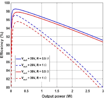
For a fixed output voltage, the efficiency is derived for different output powers from (15) and (16). Fig.7 shows the theoretical efficiency as a function of the output powers, for two output voltages and two piezoelectric damping values. The results are very promising with an efficiency higher than 95% for a very large operating range up to 1.5 W (for R = 0.5 Ω). At the same output power, the efficiency decreases when the output gain increases. The impact of R on the efficiency is illustrated by the dotted curve where this resistance has been doubled. The efficiency and maximum output power are clearly reduced when R is increased, which confirms that the material must be chosen with a mechanical resistance as low as possible, meaning a material with a high quality factor.
Fig. 5. Output voltage gain with respect to cos (ω.t4) with and without
Fig. 7. Theoretical power-efficiency curves for 2 output voltages and mechanical damping
The analytical model reveals a maximum of efficiency at a given output power and a maximum power transfer point due to the mechanical losses. There is also a maximum theoretical efficiency in classical half-bridge topology with PT [25].
1) Maximum power point and corresponding efficiency The discriminant of the quadratic equation (14) must be positive in order to get real solutions. This leads to a maximum limit for the output power Pout_max . At this maximum output
power (computed with (17)), the efficiency is given by (18).
|𝑃𝑜𝑢𝑡_𝑚𝑎𝑥 | = 𝑉𝑖𝑛2 𝑅. 𝜋 − 𝐶0. 𝜔. 𝑉𝑖𝑛. 𝑉𝑜𝑢𝑡 2. 𝜋 (17) 𝜂(𝑃𝑜𝑢𝑡_𝑚𝑎𝑥) = 1 2 −𝐶0. 𝜔. 𝐺. 𝑅. 𝜋2 1 −𝐶0. 𝜔. 𝐺. 𝑅. 𝜋 2 (18) With a traditional disc-shaped piezoelectric ceramic, the common part of the numerator and denominator of (18) is very small compared to 1 and therefore, as an impedance matching, the efficiency at maximum output power is around 50% whatever the gain. The global maximum output power is reached when the output gain G tends to 1 and equals 8.37 W with the piezoelectric element of TABLE I and an input voltage of 10 V. This global maximum output power is approximated by neglecting the second term of the numerator of (17) (8.44 W). This maximum output power depends of the square of the input voltage.
2) Maximum efficiency and corresponding power
To find the maximum efficiency ηmax, the efficiency is
expressed as a function of ∆I. Finally, the maximum output
power is calculated using (19) by finding first the power that leads to the maximum efficiency (20). At the end, this leads to a very simple expression (21) for the maximum efficiency,
which depends of the main piezoelectric parameters (C0, ω,
R) and of the desired output gain G. This simple formula makes the pre-designing fast and reliable.
𝑑𝜂 𝑑(−𝑃𝑜𝑢𝑡) = 𝑑𝜂 𝑑∆𝐼. 𝑑∆𝐼 𝑑(−𝑃𝑜𝑢𝑡) (19) 𝑃𝑜𝑢𝑡(η𝑚𝑎𝑥) = 𝐶0. 𝜔. 𝑉2. 𝜋𝑜𝑢𝑡. (𝑉𝑜𝑢𝑡. 𝐶0. 𝜔. 𝑅. 𝜋 − 𝑉𝑖𝑛) (20) η𝑚𝑎𝑥= 1 − 𝐶0. 𝜔. 𝑅. 𝜋. 𝐺 (21) The global maximum efficiency reachable with our selected ceramic is 99.1% (computed using (21) with G = 1).
3) Maximum output gain
For a given resistive load, a maximum output gain Vout_max
and therefore output power can be found choosing the appropriated t4_opt time. This is illustrated by Fig.6. To find this
maximum value, a method similar to the one expressed by (19) is used. ∆g is the discriminant of the quadratic form that appears
solving the system. g1_opt corresponds to the value of g1 from
(13) that gives the highest Vout. Vout_max is an increasing function
of RL (25) with an asymptotic limit value (27). The piezoelectric
current amplitude leading to this maximum voltage, given by (26), is independent from RL. ∆𝑔= (𝐶0. 𝜔)2+ 8 𝑅. 𝑅𝐿 (22) 𝑔1_𝑜𝑝𝑡= 𝐶0. 𝜔 + √∆𝑔 2 (23) t4_opt=𝜔1. (−𝑎𝑟𝑐𝑐𝑜𝑠(1 − 2. 𝑅𝐿. 𝐶0. 𝜔 + 4. 𝜋 𝑅𝐿. (𝐶0. 𝜔 + √∆𝑔) ) + 2. 𝜋) (24) 𝑉𝑜𝑢𝑡_𝑚𝑎𝑥 = 2. 𝑉𝑖𝑛. 𝑔1_𝑜𝑝𝑡− 𝐶0. 𝜔. 𝑉𝑖𝑛 2. 𝜋 𝑅𝐿 + 𝑅. 𝜋. 𝑔1_𝑜𝑝𝑡 2 (25) 𝐼 (𝑉𝑜𝑢𝑡_𝑚𝑎𝑥) = 𝑉𝑖𝑛 𝑅. 𝜋 (26) 𝑉𝑜𝑢𝑡_𝑚𝑎𝑥 𝑉𝑖𝑛 (𝑅𝐿→ +∞) = 1 𝑅.𝜋.𝐶0.𝜔 (27)
The higher the piezoelectric quality factor is, the higher the converter gain can be. The theoretical maximal output gain that can be reached with the chosen piezoelectric is 112. This structure can therefore theoretically achieve very large step-up operations taking great benefice from the piezoelectric high quality factor.
V. CONVERTER SIMULATION
A simulation of the converter was performed on Matlab/Simulink. The piezoelectric material is modeled using the impedance transfer function derived from the equivalent electrical circuit of Fig.4 and expressed in (28).
𝐻𝑝 (𝑗. 𝜔) = 𝑉𝑝(𝑗. 𝜔) 𝐼(𝑗. 𝜔) = 1 𝑗. 𝐶0. 𝜔. 𝜔 ) 𝑅 + 𝑗. 𝐿. 𝜔(1 − (𝜔𝜔 )𝑝 2) (28) Where ωs is the resonance pulsation and ωp the antiresonance
pulsation and are defined by:
𝜔𝑠= 1
√𝐿. 𝐶 , 𝜔𝑝= √ 𝐶 + 𝐶0
𝐿. 𝐶. 𝐶0 (29) A finite state machine is implemented via Matlab to manage the succession of the 6 phases and to define the switches states. A RL parallel CL load is chosen. A regulation loop of the output
voltage is introduced. A proportional integral (PI) corrector ensures the control of the closed loop. Since the system is highly nonlinear, the open loop gain dVout/dt4 of the systems is
obtained thanks to a linearization around the operating point. The open loop gain is therefore computed assuming a small variation ∆t4 of t4 in (12) and (13). Finally, the gains are
expressed as follows: 𝐴 = ∆𝑔1 ∆𝑡4 = (𝑅𝐿. 𝐶0. 𝜔 + 2. 𝜋). sin(𝜔. 𝑡4) . 𝜔 𝑅𝐿. (1 − cos(𝜔. 𝑡4))2 (30) = 𝑔1(𝑡4). 𝜔. cot ( 𝜔. 𝑡4 2 ) ∆𝑉𝑜𝑢𝑡 ∆𝑡4 = 𝑉𝑜𝑢𝑡 (𝑡4 + ∆𝑡4) − 𝑉𝑜𝑢𝑡(𝑡4) ∆𝑡4 = (31) 2. 𝐴. 𝑉𝑖𝑛 2. 𝜋 𝑅𝐿+ 𝑅. 𝜋. 𝑔1(𝑡4) 2(−1 + 𝑅. 𝜋.𝑔1(𝑡4). (2.𝑔1(𝑡4)−𝐶0. 𝜔) 2. 𝜋 𝑅𝐿 + 𝑅. 𝜋.𝑔1(𝑡4) 2 )
For a 400 load and with ω.t4 at 3.π/2, the gain is 13 MV.s-1.
The corrector parameters are computed from the gain value derived with (31). The regulation is not applied during the transient time of the system stating from naught because a specific control is required.
At the beginning, during the transient time, the piezoelectric current is not established and the theoretical cycle of Fig.3-b cannot be applied. To ensure the operation during the transient time, switches are turned off and turned on at their theoretical time derived from the analytical model of section IV. The resonator is then excited at its resonance frequency and therefore the piezoelectric current amplitude increases. After a certain delay, the current amplitude is sufficient to apply the cycle of Fig.3-b.
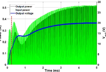
The output voltage waveform and the evolution of the piezoelectric power exchanges are given in Fig.8 for a power set of 0.5 W and a voltage ratio of 2 (Vin equals 10 Volts).
Fig. 8. Energy exchanges and output voltage during transient time
At first, the material receives many more energy than it releases meaning that the resonator accumulates energy and the output voltage rises rapidly (CL is initially discharged). After 20
resonant periods (see vertical dotted line), the normal cycle, synchronized with the current waveform, enters in operation including the closed loop that regulates the output voltage. The output voltage reaches the 20V target voltage after 4.5ms. After stabilization, the output power becomes very close to the input power, meaning that the efficiency is very close to 1.
Fig.9. presents the response of the regulation to a fast variation of a load. A change of resistive load from 800 to 1200 is applied after 4 milliseconds. In steady state, the current amplitude is around 0.15 A. This is therefore in perfect agreement with the analytical model (0.154 A using (15)). The PI corrector makes the output voltage return to 20 V, 2 milliseconds after the load change. This validates the operation principle with a response time about 20 piezoelectric periods. By using a piezoelectric having a higher resonance frequency or by using the thickness mode of the selected piezoelectric (2.8 MHz), the response time should be significantly reduced. In counterpart, the electronic management circuit needs to be faster.
Fig. 9 Piezoelectric current and output voltage: effect of a load variation
This simulation validates the analytical model and its hypothesis. It also proves the possibility of controlling the
output voltage. The simulations enable also to understand and manage the transient part since the analytical model only considers steady states operations.
VI. EXPERIMENTATIONS AND RESULTS
A. Converter presentation
The converter was fabricated and tested. A first experimentation had already been done successfully and presented in [24] with an efficiency up to 87 %. In this paper we present an update of this proof of concept with a significant improvement in term of efficiency and power level. The diodes had been replaced by MOS transistors which have been chosen for their low on-state resistance. Furthermore, the parasitic inductances of the switching paths due to the layout have been significantly reduced. A finite-state machine is used to switch from one state to another and to achieve the voltage regulation with the help of an analog to digital converter (ADC). This finite-state machine is implemented with a Field Programmable gate array (FPGA). The switch kin must be bidirectional and is
therefore composed of two N channel MOSFET kin1 and kin2
(IRLML0040TRPbF, Infineon®). Switches k3 and kout are N
channel MOSFETs as well. Nevertheless, since the 6 phases cycle must be synchronized with the piezoelectric current, a Schottky diode Dout with a lower voltage drop than the inherent
reverse diode of kout is added in parallel. Indeed, in phase 6, the
MOSFET is conducting most of the time but just before the end of the period, it is turned off to let the parallel diode conduct to have a precisely synchronized cycle. An isolated driver receives the signals from the FPGA and allows to control the switches with a valid gate-source voltage. The overall operation of the converter is resumed in Fig.10 and the picture of the power circuit is presented on Fig.11.
Fig.10. Experimental converter description
B. Experimental results
The conversion cycle was successfully reproduced and experimental waveforms are presented in Fig.12 corresponding to a 10 V-20 V, 90 kHz conversion with an output power of 310 mW. The internal piezoelectric current cannot be directly measured but it is possible to observe it during constant voltage phases measuring im. Experimental voltage (Vp) and current (im)
waveforms are compared to the one given by the analytical model including mechanical damping (section IV-B) for the same output power. The transition between the conduction of kout and Dout is observable and highlighted by the vertical dotted
line and proves that the system is well synchronized with the piezoelectric current. The experimental piezoelectric voltage waveform is very close to the theoretical one. The current is almost sinusoidal but has some harmonics contents due to the other piezoelectric resonance modes and to parasitic elements of the layout. This validates the analytical model since the current amplitude and the duration of phases are quite well corresponding.
Fig. 12. Experimental piezoelectric current and voltage waveforms for a 310 mW conversion compared to analytical model
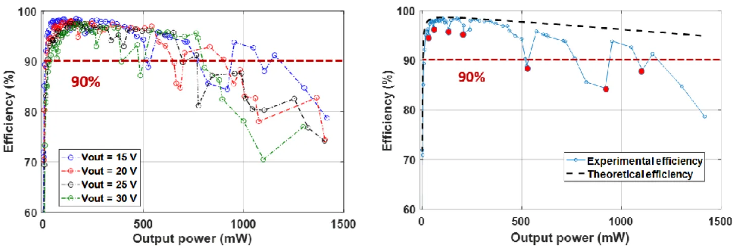
The efficiency was measured for different operating points with four different output voltages (input voltage of 10 V) and for different output powers. The power spent for the control part is not taken into account. The power efficiency graph is represented in Fig.13-a. Fig.13-b compares the power efficiency curve with the theoretical one for a step up 10-15 V converter. A high efficiency up to 98.4 % (10-15 V conversion, 160 mW) and a power conversion up to 1.45 W (10-15 V conversion, 78% of efficiency) were achieved. As expected, the efficiency remains high for a large range of power whatever the output gain ratio. The frequency has been measured for each points of Fig.13-a. It ranges from 89 to 104 kHz (resonance and anti-resonance) depending on the load and output gain. Nevertheless, since those variations have no real impact on the system behavior, the fixed frequency approximation of the analytical model remains very relevant.
The analytical model of section IV is in very good agreement with experimental results for low powers and is therefore validated. However, above 500 mW, the error increases and the efficiency drops more than expected. This can be explained considering that the piezoelectric current amplitude I increases with the power, the same for the constant voltage phase’s duration. That increases the transistor conduction losses which are not taken into account in the model, and explains the increasing gap between the model and the experimental results with the increasing power. Another cause of the difference is that for high powers, the material temperature starts rising and induces a decrease of the mechanical quality factor. Compared to the theoretical power efficiency curve, the experimental measurement reveals also irregularities at some points (big points in Fig.13 (b)) with sudden drops in efficiency for specific values of the output power. This is due to the harmonics effect discussed in the next section.
The material temperature was observed with an infrared thermometer for a 1.2 W 10-20V conversion, the measured temperature elevation is only of 11°C compared to ambient although there is no cooler. Anyhow, it is far from the material Curie temperature (315°C).
VII. DISCUSSION
A. Harmonic analysis
As mentioned previously, there are some points in the power efficiency curves where the efficiency drops suddenly before increasing again. Those irregularities which are not predicted by the model, takes greater importance considering high output powers. The reason is that the voltage Vp applied to the
resonator contains harmonics able to excite some other resonance modes of the piezoelectric material. The higher the output power is, the higher is the harmonic content, which increases the probability to encounter this problem. As a result, if the current has an important harmonic content, the transitions between the phases of the conversion cycle (based on ZVS conditions) occur at a different time compared to the sinusoidal case. Moreover, its RMS value increases, the same for losses. This creates a difference between the ideal 6 phase’s cycle of Fig.3-b and the real applied conversion cycle. To avoid these points, the condition is therefore to have no harmonics at the other resonance mode of the material. Fig.14-a and Fig.14-b compare two cases: a normal case (A case 960mW) and a case where the thickness mode is excited (B case 580 mW). The current in the B case has a significant harmonic content corresponding to the thickness resonance mode. That is why the efficiency is lower compared to the A case although the global harmonic content is higher in this case. This effect is proved in Figure 15: in case B (580 mW) it can be observed that the piezoelectric current harmonic at 2.8 MHz matches exactly the thickness mode of the impedance curve of the resonator, but not for case A.
The harmonics excitation frequencies and related level can be theoretically predicted thanks to the Fourier decomposition of the piezoelectric voltage Vp. From these frequencies and related
level, knowing the various resonance and related amplification of the piezoelectric material one can deduce the final current
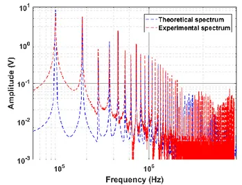
amplitude for each harmonic frequency. In Fig.16, the theoretical spectrum of Vp is compared to the measured one for
the same conditions (960 mW and 10-20 V conversion). The main frequencies peaks observed are quite well predicted by theory. The small difference is because the experimental cycle is not perfectly synchronized with the fundamental current waveform and also because some losses are not taken into account like the conduction losses in the transistors. However, some harmonic frequencies are not theoretically predicted, they are caused by parasitic elements as the stray inductance of the wires that connect the piezoelectric to the electronic. They resonate with the parallel capacitance Cp of the piezoelectric material. When designing the converter, the theoretical 6 phase’s cycle spectrum should not have a significant harmonic that matches with a higher frequency resonance mode.
B. Elements for future work
The analytical model including the mechanical damping is very relevant for a large set of operating points (until 500 mW in this case). In the first part of the power efficiency curve, it constitutes an excellent approximation of the converter keys waveforms and is therefore reliable for design issues. To be more accurate for the second part of the graph, other elements than the mechanical resistance R should be added in the model like the transistors conduction losses. The decrease of the quality factor can be modelled by making R depending on temperature. This would enable to predict the limits of the material and the maximal current it can withstand.
For design issues, the impact of geometry parameters such as the resonator diameter and thickness must be studied. This could be done by expressing each term of the piezoelectric electrical equivalent circuit as a function of the piezoelectric geometry using [26] . It should be noted that reducing the diameter increases the radial resonance frequency (control dynamic must increase) and reducing the thickness increases the thickness resonance frequency. The analytic model developed in section IV highlights the necessity of a low mechanical damping (R as low as possible). Since [26] states that R can be linearly reduced by reducing the radius or thickness of the disk, it means that theoretically, efficiency and
Fig. 14-a Case A: Piezoelectric waveforms for 960 mW
Fig. 14-b Case B: Piezoelectric waveforms for 580 mW
Fig. 15. Harmonic spectra of piezoelectric current for A and B cases: large scale and thickness mode centered
Fig. 16. Comparison of theoretical and observed harmonics of piezoelectric voltage
resonator. However, the limits of the material must also be included in the model. The converter should therefore be tested and compared for different piezoelectric sizes at different output powers and conversion ratios. Based on experimental results, efficiency and maximum output power should be expressed as a function of the resonator dimensions. A design procedure using the model described in IV and taking the material limits into consideration should be established. For a desired input and output voltage and a given output power this procedure should use (20) and (21) to optimize the efficiency or (17), (18) and thermal limits to optimize the power density.
A 1.45 Watt conversion was achieved (10-15 V conversion, 78% of efficiency) but with the same piezoelectric resonator, higher powers and therefore higher power densities can be easily reached by increasing the input voltage as (17) states.
VIII. CONCLUSION
A new piezoelectric DC-DC converter is presented. The PZT material replaces the traditional magnetic-based inductance as an energy storage element. At steady state, a conversion cycle is applied at each resonant period in which the converter’s input and output are successively connected to the material to accumulate or release energy. The driving strategy of the converter ensures both ZVS operations and output current/voltage regulation allowing to keep very high efficiencies for a large range of output gain and power. The presented analytical model, validated by simulation and experimentation, enables a fast and reliable converter predesigning. This concept has been very successfully validated getting an efficiency up to 98.4 % at 160 mW and achieving a conversion up to 1.4 W.
This new concept, being very promising, can be extended to other topologies of classical power converters based on temporary energy storage. Putting several piezoelectric resonator in parallel or operating in an interleaving mode to increase the output power, performing an AC-DC conversion or achieving an isolated piezoelectric-based converter are other possibilities that we are studying.
REFERENCES
[1] A. Vazquez Carazo, “Piezoelectric Transformers: An Historical Review,” Actuators, vol. 5, no. 2, p. 12, Apr. 2016.
[2] C. Degel et al., “3D sonar system based on mills cross antenna configuration,” in Oceans-St. John’s, 2014, 2014, pp. 1–6.
[3] D. Guyomar, A. Badel, E. Lefeuvre, and C. Richard, “Toward energy harvesting using active materials and conversion improvement by nonlinear processing,” IEEE Trans. Ultrason. Ferroelectr. Freq. Control, vol. 52, no. 4, pp. 584–595, 2005.
[4] M. J. Prieto, J. Diaz, J. A. Martin, and F. Nuno, “A very simple DC/DC converter using piezoelectric transformer,”
PESC. 2001 IEEE 32nd Annual, 2001, vol. 4, pp. 1755– 1760.
[5] T. L. A. van den Heuvel, D. J. Graham, K. J. Smith, C. L. de Korte, and J. A. Neasham, “Development of a Low-Cost Medical Ultrasound Scanner Using a Monostatic Synthetic Aperture,” IEEE Trans. Biomed. Circuits Syst., vol. 11, no. 4, pp. 849–857, Aug. 2017.
[6] M. Ekhtiari, Z. Zhang, and M. A. Andersen, “State-of-the-art piezoelectric transformer-based switch mode power supplies,” in The 40th Annual Conference of the IEEE Industrial Electronics Society, IECON, 2014, pp. 5072– 5078.
[7] E. Sarraute, D. Vasic, and F. Costa, Transformateurs statiques piézoélectriques. Ed. Techniques Ingénieur, 2005.
[8] M. Sanz, P. Alou, R. Prieto, J. A. Cobos, and J. Uceda, “Comparison of different alternatives to drive piezoelectric transformers,” in Applied Power Electronics Conference and Exposition, 2002. APEC 2002. Seventeenth Annual IEEE, 2002, vol. 1, pp. 358–364. [9] R. L. Lin, F. C. Lee, E. M. Baker, and D. Y. Chen,
“Inductor-less Piezoelectric Transformer Electronic Ballast for linear fluorescent lamp.”, in Proceedings of Applied Power Electronics Conference. APEC '2001, Anaheim, CA, United States, pp 664-669.
[10] S. Bronstein and S. Ben-Yaakov, “Design considerations for achieving ZVS in a half bridge inverter that drives a piezoelectric transformer with no series inductor,” in Power Electronics Specialists Conference, 2002. pesc 02. 2002 IEEE 33rd Annual, 2002, vol. 2, pp. 585–590. [11] M. Ekhtiari, Z. Zhang, and M. A. E. Andersen, “Analysis
of Bidirectional Piezoelectric-Based Converters for Zero-Voltage Switching Operation,” IEEE Trans. Power Electron., vol. 32, no. 1, pp. 866–877, Jan. 2017.
[12] E. L. Horsley, A. V. Carazo, Nam Nguyen-Quang, M. P. Foster, and D. A. Stone, “Analysis of Inductorless Zero-Voltage-Switching Piezoelectric Transformer-Based Converters,” IEEE Trans. Power Electron., vol. 27, no. 5, pp. 2471–2483, May 2012.
[13] M. P. Foster, J. N. Davidson, E. L. Horsley, and D. A. Stone, “Critical Design Criterion for Achieving Zero Voltage Switching in Inductorless Half-Bridge-Driven Piezoelectric-Transformer-Based Power Supplies,” IEEE Trans. Power Electron., vol. 31, no. 7, pp. 5057–5066, 2016.
[14] J.-H. Park, G.-S. Seo, B.-H. Cho, and K.-P. Yi, “A
Resonant-type Step-up DC/DC Converters with
Piezoelectric Transducer,” Trans. Korean Inst. Power Electron., vol. 14, no. 5, pp. 343–354, 2009.
[15] S. Moon and J.-H. Park, “High Power DC–DC Conversion
Pb(Zr,Ti)O$_{3}$ Ceramic Transducer,” Jpn. J. Appl. Phys., vol. 50, no. 9, p. 09ND20, Sep. 2011.
[16] K. W. E. Cheng, “Zero-current-switching switched-capacitor converters,” IEE Proc. - Electr. Power Appl., vol. 148, no. 5, p. 403, 2001.
[17] T. Zaitsu, T. Shigehisa, M. Shoyama, and T. Ninomiya, “Piezoelectric transformer converter with PWM control,” in Proceedings of Applied Power Electronics Conference. APEC ’96, San Jose, CA, USA, 1996, vol. 1, pp. 279–283. [18] S. Hamamura, T. Ninomiya, M. Yamamoto, and M. Katsuno, “Combined PWM and PFM control for universal line voltage of a piezoelectric transformer off-line converter,” IEEE Trans. Power Electron., vol. 18, no. 1, pp. 270–277, Jan. 2003.
[19] J. A. Martin-Ramos, M. A. J. Prieto, F. N. Garcia, J. D. Gonzalez, and F. M. F. Linera, “A new full-protected control mode to drive piezoelectric transformers in DC-DC converters,” IEEE Trans. Power Electron., vol. 17, no. 6, pp. 1096–1103, Nov. 2002.
[20] M. Ekhtiari, T.-G. Zsurzsan, M. A. E. Andersen, and Z. Zhang, “Optimum Phase Shift in the Self-Oscillating Loop for Piezoelectric-Transformer-Based Power Converters,” IEEE Trans. Power Electron., vol. 33, no. 9, pp. 8101– 8109, Sep. 2018.
[21] M. Khanna, R. Burgos, Q. Wang, K. D. T. Ngo, and A.
Vazquez Carazo, “New Tunable Piezoelectric
Transformers and Their Application in DC–DC Converters,” IEEE Trans. Power Electron., vol. 32, no. 12, pp. 8974–8978, Dec. 2017.
[22] J. Mark Noworolski and Seth R. Sanders, “Microresonant devices for power conversion,” in Proc. SPIE Micromachined devices and Components IV, 1998, vol. 3514, pp. 3514–6.
[23] S. Ghandour, G. Despesse, and S. Basrour, “Design of a new MEMS DC/DC voltage step-down converter,” in NEWCAS Conference (NEWCAS), 2010 8th IEEE International, 2010, pp. 105–108.
[24] B. Pollet, F. Costa, and G. Despesse, “A new inductorless DC-DC piezoelectric flyback converter,” in proceedings of IEEE International Conference on Industrial Technology, ICIT 2018, pp. 585–590.
[25] Y.-P. Liu, D. Vasic, F. Costa, W.-J. Wu, and C.-K. Lee, “Design of fixed frequency controlled radial-mode stacked disk-type piezoelectric transformers for DC/DC converter applications,” Smart Mater. Struct., vol. 18, no. 8, p. 085025, Aug. 2009.
[26] R.-L. Lin, “Piezoelectric transformer characterization and application of electronic ballast,” Ph.D. dissertation, Electrical Engineering Department, Virginia Tech, 2001.