HAL Id: hal-03047670
https://hal.archives-ouvertes.fr/hal-03047670
Submitted on 8 Dec 2020
HAL is a multi-disciplinary open access archive for the deposit and dissemination of sci-entific research documents, whether they are pub-lished or not. The documents may come from teaching and research institutions in France or abroad, or from public or private research centers.
L’archive ouverte pluridisciplinaire HAL, est destinée au dépôt et à la diffusion de documents scientifiques de niveau recherche, publiés ou non, émanant des établissements d’enseignement et de recherche français ou étrangers, des laboratoires publics ou privés.
The effect of N-vacancy and In aggregation on the
properties of InAlN
Ranim Mohamad, Jun Chen, Pierre Ruterana
To cite this version:
Ranim Mohamad, Jun Chen, Pierre Ruterana. The effect of N-vacancy and In aggregation on the properties of InAlN. Computational Materials Science, Elsevier, 2020, 172, pp.109384. �10.1016/j.commatsci.2019.109384�. �hal-03047670�
Manuscript ID: COMMAT-D-19-01731R1
Titled: The effect of N-vacancy and In aggregation on the properties of InAlN.
1 2 3 4 5 6 7 8 9 10 11 12 13 14 15 16 17 18 19 20 21 22 23 24 25 26 27 28 29 30 31 32 33 34 35 36 37 38 39 40 41 42 43 44 45 46 47 48 49 50 51 52 53 54 55 56 57 58 59 60
The effect of N-vacancy and In aggregation on the properties of InAlN
Ranim Mohamad*, Jun Chenand Pierre Ruterana
Centre de Recherche sur les Ions, les Matériaux et la Photonique UMR 6252, CNRS ENSICAEN UCBN CEA, 6 Boulevard du Maréchal Juin, 14050 Caen Cedex, France.
In0.17Al0.83N, lattice matched to GaN, is an attractive solution for applications such as high electron
mobility transistors, distributed Bragg reflectors, or light-emitting diodes. It has been reported that InAlN layers lattice matched to GaN on growth along the [0001] exhibit crystallographic degradation when the thickness is increased. In our recent work, it was shown, through theoretical modelling as well as transmission electron microscopy, that the N vacancy (VN) plays a critical role in this behavior. In
this work, we have carried out a detailed theoretical investigation of the possible modification of the properties of this alloy as brought about by the presence of the nitrogen vacancy and the associated formation of the indium rich regions. After testing the ab initio procedures on the AlN and reproducing the lattice parameters and band gap with high accuracy, it is shown that the indium aggregation in InAlN leads to a reduction of the band gap. In contrast to AlN, where acceptor levels can also form, the combination of the nitrogen vacancy and the favored indium aggregation introduced even more levels at the top of the band gap, moreover examining the whole spin configuration we find a strong asymmetry in the occupation of the spin up and down states with a net moment of around 1 µB per supercell. Most importantly, the presence of a nitrogen vacancy changes significantly the top of the band gap: first, the band edges become very sharp, and second, the introduced states originating from local deformation are occupied. This leads to n type doping of the alloy and nicely agree with the use of Ti for generation of N vacancies in the technology of ohmic contacts on nitride materials.
*Manuscript
2 3 4 5 6 7 8 9 10 11 12 13 14 15 16 17 18 19 20 21 22 23 24 25 26 27 28 29 30 31 32 33 34 35 36 37 38 39 40 41 42 43 44 45 46 47 48 49 50 51 52 53 54 55 56 57 58 59 60 61 I. Introduction
III-V semiconductor (AlN, GaN, InN) have unique physical properties such as high electron mobility, high saturation velocity, direct and tunable band gaps (6.2 to 0.65 eV), large absorption coefficients and high thermal stability as well as good thermal conductivity. These outstanding properties have allowed them to come at the forefront of optical applications in light emitting diodes (LEDs) [1] and laser diodes (LDs) [2], as well as in microelectronics as high frequency, high power devices (high electron mobility transistors (HEMT)) [3]. Of particular interest is the InAlN alloy, where, close to 18% of In-content, the lattice match to GaN can be achieved with a band gap around 4.2eV and the performances of the corresponding HEMTs are expected to improve by avoiding the interface strain due to the lattice mismatch which is inherent in AlGaN/GaN heterostructures [4]. Moreover, it has been shown that the HEMTs with an InAlN barrier can operate at very highest frequencies (~ 300 GHz) and withstand temperatures up to1000 °C [5]. Still, many challenges need to be addressed, as the performance of the corresponding devices strongly depends on the materials quality of active layers which are grown on foreign substrates. These layers may contain extended defects such as dislocations [6], stacking faults [7, 8] and inversion domains [9], but also point defects all of which have a spurious influence on the device performance and stability [10, 11, 12]. More specifically, in addition to the above-mentioned defects, InAlN layers have been shown to undergo extensive crystallographic degradation with increasing thickness [13, 14] and some mechanisms have been proposed in order to explain this behavior. For instance, Chen et al. [13] reported that the threading dislocations (TD) propagating from the underlying GaN layer may be at the origin of a TD governed degradation of the InAlN layers with increased thickness through the formation of V-pits. However, in their work on self-supported low dislocation density InAlN/GaN heterostructures, Perillaz-Merceroz et al. reported a similar degradation of the ternary layers [14] under compressive and tensile strain state. This was then attributed to the particular growth mode of InAlN which is dominated by kinetic roughening and formation of hillocks at the
2 3 4 5 6 7 8 9 10 11 12 13 14 15 16 17 18 19 20 21 22 23 24 25 26 27 28 29 30 31 32 33 34 35 36 37 38 39 40 41 42 43 44 45 46 47 48 49 50 51 52 53 54 55 56 57 58 59 60
growing surface. The V-defects were then shown to appear above a critical thickness which depended on the growth conditions and they were proposed to correspond to stabilized inclined facets of hillocks. In our current investigations and by carefully examining the results of the literature, we became convinced that probably the coalescence of growth hillocks is not the most predominant origin of the V-defects, as they start to form on the tops of hillock, and not between [14]. Moreover, each crystallographic defect can influence in a typical way the observed degradation of the InAlN/GaN layers [15] and it is not clear that even for the spontaneous degradation, a critical thickness can be accurately determined [16]. As reported more recently, this degradation may also be related to local indium segregation which has been shown to be favorable when relaxing the strain which is introduced in the system by N-vacancies [16].
In this work, we have investigated, in detail, the possible influence of the In aggregation and N-vacancy on the electronic properties of InAlN alloys. Earlier, the role of indium clustering on the band structure of InxAl1-xN alloys was investigated by Gorczyca et al. [17] by ab-initio methods using
supercell geometry with 32 atoms and the effects of varying the composition and atomic arrangements were examined. It was reported that the In clustering influences the band gap which becomes smaller. In the present paper we present the electronic properties in two case, 1- In aggregation in InAlN and 2- In aggregated around a VN situated in the center of supercell, inside the InAlN alloy. To this end, we have
first calculated the properties of the bulk AlN, using the Heyd Scuseria Ernzerhof (HSE) functional to verify the robustness of our procedures by comparing with the experimental data. Subsequently, we investigated the effect of VN and aggregation of In on electronic and magnetic properties of the InAlN
alloy, in this procedure, their influence on localization of electron was also determined.
II. Computational details
With the objective of investigating the properties of native defects in InAlN and determining how the nitrogen vacancy may affect its electronic properties, we carried out the structural relaxations within
2 3 4 5 6 7 8 9 10 11 12 13 14 15 16 17 18 19 20 21 22 23 24 25 26 27 28 29 30 31 32 33 34 35 36 37 38 39 40 41 42 43 44 45 46 47 48 49 50 51 52 53 54 55 56 57 58 59 60 61
the density functional theory as implemented in the Vienna ab initio simulation package (VASP) [18] with the projector augmented wave (PAW) method [19], using supercells of 128 atoms which correspond to 4 4 4 unit cells. In these systems, the (In, Al) and N atoms occupy, respectively, the two hexagonal close packed sublattices of the corresponding wurtzite structure which belongs to the P6/3mc space group [20]. The indium concentration of x=17.2%, has been realized by substituting 11 Al
atoms by In in the supercell. We investigated two atomic distributions: 1) the uniform alloy in which the positions of the metal atoms were randomly distributed, 2) and the clustering case in which Al atoms in the center of the supercell were substituted by In. The calculations have been performed in two steps, applying two different approximations in order to improve the accuracy as it is well known that the LDA (Local Density Approximation) underestimate the band gap of semiconducting materials. As a first step, the initial atomic coordinates in the supercell were relaxed by minimization of the Hellmann-Feynman forces (smaller than 10-7 eV. Å-1) for each configuration using the GGA (Generalized Gradient
Approximation) [21] for the exchange-correlation term. To this end, a cutoff energy of 900 eV for the plane wave basis set was sufficient for attaining converged results and a k-point mesh of Monkhorst-Pack [22] special points was used. The relaxations were performed until the energy on each ion was smaller than 10-6 eV.
In the second step, the aim was to improve the accuracy of the results from the GGA; to this end, we used the HSE06 (Heyd-Scuseria-Ernzerhof) functional to correct the band gap, and the convergence criteria was that the force and energy were smaller than 0.02 eV. Å-1 and 10-4 eV, respectively. The accuracy of the HSE functional is determined by the two parameters, α and ω, which are the fractions of semi local Perdew–Burke–Ernzerhof (PBE) functional replaced by a screened nonlocal functional and the inverse screening length, respectively [23]. In this study, α and ω are set at 25% and 0.2Å-1,
respectively, which correspond to the HSE06 functional [24]. For calculating the density of state (DOS) of structures, a k-point mesh of Monkhorst-Pack was used. Clearly, there is a notable
2 3 4 5 6 7 8 9 10 11 12 13 14 15 16 17 18 19 20 21 22 23 24 25 26 27 28 29 30 31 32 33 34 35 36 37 38 39 40 41 42 43 44 45 46 47 48 49 50 51 52 53 54 55 56 57 58 59 60
difference between the two steps, and as can be seen in table 1, our second step gives values of the band gap for AlN which are close to the published experimental [25] results within 1.8%, whereas the GGA approximation band gap falls away by 34%.
Table 1: Bulk AlN lattice constants ( and ), and electronic band gap ( ), of AlN as calculated using GGA-PBE and HSE06 functional along with the experimental measurements taken from references [25] and [26].
GGA HSE06 AlN Calculated 3.130 5.011 4.095 3.117 5.000 6.300 Experimental 3.1[26] 4.980 [26] 6.190 [25] III. Results III.1. AlN
Before addressing the InAlN alloy, we found useful to test our procedures on AlN. Indeed, for this compound many experimental and theoretical data are available in the literature. For that, a supercell with configuration AlN was simulated using the procedure described in section II. The relaxed equilibrium Al-N bond length of 1.91 Å and the lattice parameter of 3.117 Å are close to the experimental value (3.110 Å) [26] and previous theoretical work [27, 28]. As can be seen in the electron localization function (ELF) [29] (figure 1), electron rich areas (red to green) are located around the nitrogen atoms (small spheres), meaning that there is a charge transfer from the Al atoms (large spheres) to N and therefore the bond between the two elements has a strong ionic character. This of course is due to the electronegativity difference between Al and N.
2 3 4 5 6 7 8 9 10 11 12 13 14 15 16 17 18 19 20 21 22 23 24 25 26 27 28 29 30 31 32 33 34 35 36 37 38 39 40 41 42 43 44 45 46 47 48 49 50 51 52 53 54 55 56 57 58 59 60 61
Figure 1: The two dimensional (2D) contour slice of ELF projected on a (0001) atomic plane, Al and N atoms are shown by large and small spheres, respectively
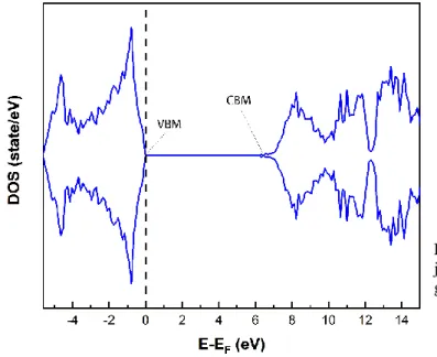
The spin polarized density of states for a perfect structure of AlN after structural optimization is exhibited in figure 2. The fermi level (dashed line) is located inside the band gap; the spin up and spin down states are totally symmetric as expected for a nonmagnetic semiconductor. The band gap width is 6.3 eV which is quite close (1.8%) to the experimental value of 6.19 eV as reported by Schulz et al. [25].
Figure 2: DOS of pure AlN, the Fermi level is located just at the top of the valence band (VBM), and the band gap is 6.3 eV (see Conduction band minimum: CBM).
If now VN is introduced in the middle of the AlN bulk supercell, the 0.73 ELF isosurface allows to
clearly visualize the asymmetry in the electron density around the vacancy. In this area, the ELF within the structure viewed along the [11-20] direction shows two high electron density zones. All of them are along the [0001] axis, however not on top of one another. Indeed, considering the tetrahedral site, which was previously occupied by the removed nitrogen atom, this represents the final redistribution of the electron density. There are definite areas of high electron density (yellow), first along the [0001] Al dangling bond and, second, in the barycenter of the three Al atoms of the top edges of the corresponding tetrahedron around the VN (Fig. 3).
2 3 4 5 6 7 8 9 10 11 12 13 14 15 16 17 18 19 20 21 22 23 24 25 26 27 28 29 30 31 32 33 34 35 36 37 38 39 40 41 42 43 44 45 46 47 48 49 50 51 52 53 54 55 56 57 58 59 60
Figure 3: ELF 0.73 isosurface for the structure viewed along [11-20], the yellow features mark the high electron density areas and the VN position is shown by the black asterisk *, the Al atoms underlined with a yellow cross are those around the VN.
As can be seen in figure 4, the 2D ELF contour of AlN underlines the location of the highest density as seen inside the (0001) plane around VN. Considering the 4 Al atoms located at the edges of the
tetrahedron centered of VN, figure 4a shows the charge distribution between the three Al atoms of the
top base of the tetrahedron (1, 2, 3). The charge density is highest at the barycenter of these three Al atoms, and equally spread towards each of them. Moreover, the distance between these atoms is around 3 Å, which slightly smaller than the 3.1 Å in the case when there is no VN. This charge density
distribution along with the shrinking of distance between these Al is a strong indication that these atoms form chemical bonds. Looking now from the bottom, there is another high electron density area on top of the fourth Al atom which means that this Al atom has a dangling bond (Fig. 4b).
2 3 4 5 6 7 8 9 10 11 12 13 14 15 16 17 18 19 20 21 22 23 24 25 26 27 28 29 30 31 32 33 34 35 36 37 38 39 40 41 42 43 44 45 46 47 48 49 50 51 52 53 54 55 56 57 58 59 60 61
Figure 4: The 2D contour slices of ELF crossing (0001) atomic plane for AlN with a VN. a) Formation of bonds between the three Al atoms, b) The possible dangling bond for the Al atom along the [0001] axis.
Figure 5 shows the calculated total DOS (TDOS) of AlN with a VN and as well as the contributions of
the valence orbitals of the two atoms (Al and N). First, as related to the bulk AlN, the band gap width has been decreased by the introduction of the nitrogen vacancy, it goes from 6.3 eV to less than 5 eV (4.96). The question, what is the origin of this band gap reduction? Looking at the valence band of AlN (Fig. 2) and after the introduction of the VN (Fig. 4a), it can be seen that the band width does not change,
therefore, this reduction of more than 1 eV in the band gap comes from changes at the bottom of the conduction band as brought in by the introduction of the N vacancy. Considering the partial densities of stated, it could be seen that the main contribution at the top of the valence band comes from the N-p orbitals, and that the bottom of the conduction band is slightly dominated by the N-s and Al-s contributions. Interestingly, additional levels are formed inside this band gap where one shallow level with spin up forms at the top of the valence band, while two deep ones are present just above the middle of the band gap. The state closest to the middle of the band gap is contributed by all the considered orbitals. Two spin down states are also present, one just at the top of the valence band the other at the highest position inside the band gap. They are both contributed by N-p and Al-s orbitals, but the highest in the band gap also receives contributions from N-s and Al-s. The calculations show that the state closest to the middle of the band gap with spin up is occupied which means that the Fermi level of the AlN-VN has almost shifted from a neutral semiconductor to one with deep donor states.
2 3 4 5 6 7 8 9 10 11 12 13 14 15 16 17 18 19 20 21 22 23 24 25 26 27 28 29 30 31 32 33 34 35 36 37 38 39 40 41 42 43 44 45 46 47 48 49 50 51 52 53 54 55 56 57 58 59 60
Figure 5: Density of state curves for AlN with VN: a) The total
DOS along with the N and Al contributions, b) The partial DOS of the Np orbitals, with a strong contribution at the top of the valence band, c) The Al-s, N-s and Al-p partial DOS have a slightly lower contribution in the valence and conduction bands, but participate equally as N-p to the deep levels inside the band gap.
From the above results, the equilibrium Al-N bond length of 1.91 Å and the lattice parameter of 3.117 Å agree with the experimental values [26]. This also the clear for the calculated the band gap of 6.3 eV which is very close to values reported in the literature of 6.0-6.3eV [30, 31,32, 33, 34, 35], and closer than the theoretical value calculated by HSE functional of 5.71 eV [28] and GGA+U functional of 4.326 [36]. Therefore, in the following, we will use the same procedure to investigate the properties of the lattice matched InAlN alloys which is very rich in Al.
III.2. InAlN
The In0.17Al0.83N alloy, which is lattice matched to GaN, was then investigated in three
configurations (see fig. 6) , first as a random alloy, then the properties of In aggregation as formed in the center of the supercell, and finally the influence of the nitrogen vacancy and its coexistence with the In.
2 3 4 5 6 7 8 9 10 11 12 13 14 15 16 17 18 19 20 21 22 23 24 25 26 27 28 29 30 31 32 33 34 35 36 37 38 39 40 41 42 43 44 45 46 47 48 49 50 51 52 53 54 55 56 57 58 59 60 61
atoms, meaning that the total number of indium atoms was always 11, and the aggregation of In was realized by exchanging In with the Al atoms closest to the supercell center.
Figure 6: The three configurations, a) random alloy, b) In aggregation as formed in the center of the supercell, and c) nitrogen vacancy and its coexistence with the In, * shows the position of the vacancy.
III.2.1. Lattice parameters
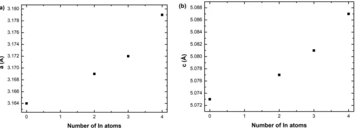
For the first two configurations (random alloy and In aggregation) the equilibrium lattice parameters of the above supercells were calculated. We have three cases, in the random alloy, a nitrogen atom can only be bound at most to one indium. In this work, we address the effect of In by discussing the three cases where the N atom is bounded to two, three and four indium atoms. For each case, the structures were relaxed by minimizing the total energy leading to the optimal atomic coordinates and , parameters of the supercell. As can be seen in Figure 7a, which shows the variation of lattice parameter, it increases with the number of In atoms around one N from 3.164 Å in the random In0.172Al0.828N alloy to 3.179 Å with an aggregation of 4 In atoms, corresponding to a change of 0.5%. A
similar behavior occurs also for (Fig. 7b), it is 5.073 Å (random alloy) and it increases to 5.087 Å when 4 In are brought around the N atom in the middle of the supercell which corresponds to a slightly lower variation of 0.3%.
2 3 4 5 6 7 8 9 10 11 12 13 14 15 16 17 18 19 20 21 22 23 24 25 26 27 28 29 30 31 32 33 34 35 36 37 38 39 40 41 42 43 44 45 46 47 48 49 50 51 52 53 54 55 56 57 58 59 60
Figure 7: The equilibrium lattice parameters (a) and (b) for InAlN versus the number of In atoms inside the In-rich region. Four In distributions in the supercell are considered: uniform and 3 aggregates (2, 3 and 4 In around a N atom in the center of the supercell).
III.2.2 Electronic structure
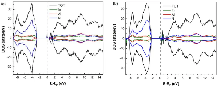
We now discuss the electronic properties for the random alloys and when indium atoms are aggregated around the N atom in the middle of the supercell, we typically take into account only 2 and 4 In atoms. As can be seen in figure 8, the most striking effect is the evolution of the band gap width, indeed band gap is largest for the uniform distribution, 4.4 eV (Fig. 8a) which maybe compared to the published experimental value of optical band gap at the composition of 17-18% (4.3 eV) [37]. When the indium is aggregated around the nitrogen atom, the calculated band gaps are 4.1 eV and 3.8 eV for 2 and 4 In atoms, respectively.
The Fermi level is always at the top of the valence band and the shape of the bands can be seen to change with the largest modification coming from the bottom of the conduction band. Therefore, the aggregation of the In atoms decreases Eg through this modification in the conduction band. Indeed, though we have only one large state at the BCM in the random alloy, three bands have been formed when 4 indium atoms are aggregated. This effect has been reported in reference [17] they conclude that the indium clustering strongly influences the band gap, for a system with 32 atoms. As in the case of
2 3 4 5 6 7 8 9 10 11 12 13 14 15 16 17 18 19 20 21 22 23 24 25 26 27 28 29 30 31 32 33 34 35 36 37 38 39 40 41 42 43 44 45 46 47 48 49 50 51 52 53 54 55 56 57 58 59 60 61
pure AlN, in these relaxed structures of In0.172Al0.828N, the electron distribution shows a predominant
localization on the nitrogen atoms (Fig. 8b), this can be explained by the fact that the electronegativity of N (3.04) and larger than that of Al (1.61) or In (1.78). Based on Bader charge analysis, the Al (In) atom loses 2.4 e (1.3 e) to the neighboring N atoms; therefore, the Al-N bond is mainly ionic whereas the In-N bond is of covalent character, along a slightly less ionic character. This is also clearly visible in the ELF image of the InAlN random alloy (Fig. 8b) where the contrast between In and N atoms indicates that the two atoms share electrons.
The total DOS reveals that the spin-up states and spin down states are symmetric, therefore the InAlN with and without In aggregation are nonmagnetic materials.
Figure 8: (a) DOS for the random distribution of In, (b) the corresponding 2D contour slice of ELF crossing (0001) atomic plane, (c) DOS of cell with 2 In atoms around the central N atom, (d) the case of 4 In atoms.
III. 2. 3. InAlN with N-vacancy
In our recent work, it was shown that the nitrogen vacancy plays an important role on the distribution of indium atoms inside the InAlN alloys [16]. In the following section, we discuss the effect
2 3 4 5 6 7 8 9 10 11 12 13 14 15 16 17 18 19 20 21 22 23 24 25 26 27 28 29 30 31 32 33 34 35 36 37 38 39 40 41 42 43 44 45 46 47 48 49 50 51 52 53 54 55 56 57 58 59 60
of VN in the middle of the calculation supercell and indium distribution on the properties of lattice
matched InAlN alloy.
III. 2. 3. 1. Electronic properties
When the N vacancy is introduced in the alloy, as can be seen in figure 9a, in comparison to the random alloys, the CBM, becomes as well defined as the VBM and clear band gap can be estimated (4.15 eV). In contrast to the case of AlN, there does not form any acceptor level close to the VBM. However, donor levels are now present just below the CBM, and the first of them is occupied which defines the new Fermi level. Two donor states are clearly visible, they can be attributed to the atoms around the vacancy because they belong only to Al and N, and as no In is present at this location, and its contribution to these states is zero. When Indium atoms are brought to substitute Al around VN, the intensity of states
slightly decreases at the Fermi level and more states appear just above, instead of one additional state in the case of the vacancy alone, there appear one state with the spin up, and two states with the spin down in the case of two indium atoms. In the case of 4 indium atoms we have a more complex configuration with the level at the Fermi level still decreasing in intensity; above it, there are now three states with the spin up and 4 levels with the spin down. These levels are now only contributed by indium and N orbitals.
2 3 4 5 6 7 8 9 10 11 12 13 14 15 16 17 18 19 20 21 22 23 24 25 26 27 28 29 30 31 32 33 34 35 36 37 38 39 40 41 42 43 44 45 46 47 48 49 50 51 52 53 54 55 56 57 58 59 60 61
Figure 9: The TDOS: a) the random alloy with a VN, b) 4 In atoms around VN.
As can be seen in figure 10, the 2D ELF crossing (0001) atomic plane shows that the metal atoms around the vacancy establish bonds between them which may explain the changes that take place on the density of states at the top of the band gap. In the case of the random alloy with 4 Al atoms around the VN, two metallic bonds Al-Al were formed between the closest atoms, the distance between 1-2 and 3-4
are 2.92 Å and 2.84 Å respectively; the distance is larger between 1-3, 2-4, 2-3, and 1-4 atoms. This is similar when In atoms are aggregated around the VN, bonds were established between the closest atoms
with a length of 2.83 Å (1-3) and 2.92 Å (2-4) for the case of 4 In atoms as this is smaller than the In-In bond length in metallic indium (3.25Å).
2 3 4 5 6 7 8 9 10 11 12 13 14 15 16 17 18 19 20 21 22 23 24 25 26 27 28 29 30 31 32 33 34 35 36 37 38 39 40 41 42 43 44 45 46 47 48 49 50 51 52 53 54 55 56 57 58 59 60
Figure 10: The 2D ELF contour of InAlN around the VN; a) Random alloy View from the top with bonding of Al (1) and Al
(2) (b) view from the bottom of the supercell showing the bonding of Al (2) with Al (4) ; c) 4 In atoms around VN, View
from the top with bonding of In (1) and In (3) (d) view from the bottom of the supercell showing the bond between In (2) and In (4)
III.2. 3.2. Magnetic properties
In comparison with AlN where the VN has been reported to introduce non-symmetric density of states
when the spin is considered [35], the above calculations were also carried out with spin polarization for InAlN. As already mentioned above, we do not have symmetry in the additional states that are introduced inside the band gap for spin up and down. Moreover, while the TDOS is completely symmetric when there is no N-vacancy (Fig. 8a), the VN induces up to a total magnetic moment of 1.00
2 3 4 5 6 7 8 9 10 11 12 13 14 15 16 17 18 19 20 21 22 23 24 25 26 27 28 29 30 31 32 33 34 35 36 37 38 39 40 41 42 43 44 45 46 47 48 49 50 51 52 53 54 55 56 57 58 59 60 61
that the systems are more stable in comparison with their counter parts when the spin polarization is not taken into account.
Table 2: Energy difference between the spin-polarized (Esp) and spin-unpolarized (Espun) states (ΔE = Espun- Esp) and magnetic moments of the supercell Mtot.
To better understand the distribution of magnetic moments in the considered systems with VN, the
local magnetic moment on each atom is shown in Table 3 where the most contributing atoms have been numbered. We then show in figure 11 the corresponding atoms for InAlN with 4 In around the VN. It is
clear that the most contributing atoms are those located around the VN.
Table 3: Local magnetic moment (µB) in InAlN alloy for random and aggregation distribution of indium.
Figure 11: The atoms that most contribute to spin polarization are those around the VN for the case with 4 indium atoms
around the vacancy.
Models ΔE(eV) Mtot(μB)
N-vacancy in InAlN 0.88 0.84
N-vacancy in InAlN + 2In 1.11 1.10
N-vacancy in InAlN + 4In 0.28 1.10
Local magnetic moment ( µB)
Number of atom VN in InAlN VN in InAlN+2In VN in InAlN+4In
1 0.048 0.137 0.149
2 0.036 0.124 0.084
3 0.022 0.050 0.123
2 3 4 5 6 7 8 9 10 11 12 13 14 15 16 17 18 19 20 21 22 23 24 25 26 27 28 29 30 31 32 33 34 35 36 37 38 39 40 41 42 43 44 45 46 47 48 49 50 51 52 53 54 55 56 57 58 59 60
IV. Discussion and conclusion
Before investigating the properties of the InAlN alloy, we tested our procedures on AlN which exist in bulk and whose properties are well known [26]. As presented above, our calculations give values which completely agree with the available experimental results (bond length, lattice parameters, band gap width). Interestingly, it is shown that the N vacancy introduces many states in the band gap which are contributed by the atoms closest to the vacancy and this is in agreement with previous reports [36]. These results on AlN are closer to the experimental results that other theoretical values calculated by HSE functional of 5.71 eV [28] or indeed GGA+U functional of 4.326 [36]. As a consequence, we confidently applied the same procedures to the InAlN as lattice matched to GaN which does not exist in bulk, and whose properties have not yet been subjected to extensive investigation with similar accuracy.
For the In (17-18%)AlN alloy lattice parameters, we obtained = 3.165 Å for the random In distribution and up to 3.179 Å for the 4 In atoms aggregation around the central N atom. The corresponding parameters were = 5.073 Å and 5.087 Å, respectively. This is very close to the experimental results as we keep the composition of 18% In where the a parameter is that of GaN and the reported (In(17.7%)AlN) = 5.089 Å [38]. Unfortunately, it is difficult to compare with the values reported in reference [17], where the lattice parameters seem to present a slight decreasing trend, as the so called clustering appears probably to some ordering, indeed the indium atoms were positioned in every 4 hexagonal layer of their supercell. The calculated DOS of random InAlN showed that the band gap width of 4.4 eV is in good agreement with the experimental measurement of 4.3 eV [37]. In addition, the In segregation with 2 In or 4 In atoms reduces the band gap width from 4.4 eV (random) to 4.1 eV (with 2 In), and 3.8 eV (4In). A similar trend was reported by Gorczyca et al. [17] who carried out LDA-LMTO (linear muffin-tin-orbital) calculations on supercells of 32 atoms, for the InxAl1-xN
(x=19%) using three configurations, their random case is similar to ours, and their band gap was 4.2 eV, in the case of 4 indium atoms around a nitrogen one, their band gap slightly decreases to 4.0 eV [17].
2 3 4 5 6 7 8 9 10 11 12 13 14 15 16 17 18 19 20 21 22 23 24 25 26 27 28 29 30 31 32 33 34 35 36 37 38 39 40 41 42 43 44 45 46 47 48 49 50 51 52 53 54 55 56 57 58 59 60 61
In our recent study [16], our theoretical modelling showed that in the presence of nitrogen vacancy, indium nitride clusters are energetically stable up to diameters around 1.4 nm. In parallel, Z-contrast TEM (Transmission Electron Microscopy) observations close to the InAlN/GaN interface confirmed that 2–5 nm size indium rich areas form and are systematically connected to the vertical degradation channels. Therefore, the VN can play an important role on this specific crystallographic
degradation in lattice matched InAlN. In this work, the modifications of the electronic properties of the InAlN alloys as contributed by the VN have been investigated in detail. It should also be pointed out that
our calculations have been carried out considering spin polarization which shows the non-symmetry of spin up and down and it is comes out that the states that are introduced inside the band gap bring about a magnetic moment of 1.00 µB. As seen above, when the VN was introduced in the InAlN ternary alloy,
the density of states changes completely, especially at the top of the band gap. As compared to the random alloy or even with indium aggregation cases, the bottom of the conduction band becomes well defined similar to the top of the valence band, and there is no significant trend for the slight change of the band gap width (4.15 eV (random case), 4.04 eV (2 In) to 4.24 eV (4 In)). Around the vacancy, metallic bonds were formed with a length of 2.84 - 2.91 Å for In-In and Al-Al which is smaller than the equilibrium distance In-In = 3.25 Å and very close to Al-Al bond (2.86 Å). Indeed, this falls in the attractive area for an In-rich cluster with a radius smaller than 6 Å as reported recently [16].
More importantly, many donor states form just below the conduction band minimum, in agreement with reports for example on AlN [35, 38]. This result is important as it explains why the enrichment of nitride layers in nitrogen vacancies turn them into n+ doped which find application for instance in the mechanism which governs the Ohmic contacts for HEMTs through the use of Ti which captures nitrogen atoms [40, 41].
In summary, we have performed a comprehensive study of the properties of lattice matched InAlN to GaN in the presence of the N-vacancy, using first-principles calculations. It is shown that the presence
2 3 4 5 6 7 8 9 10 11 12 13 14 15 16 17 18 19 20 21 22 23 24 25 26 27 28 29 30 31 32 33 34 35 36 37 38 39 40 41 42 43 44 45 46 47 48 49 50 51 52 53 54 55 56 57 58 59 60
of the N-vacancy modifies the electronic properties of the alloy; it introduces states in the band gap and moves the fermi level from the VBM toward the CBM. Taking into account the total spins shows that the system is in fact a non-symmetric in spin-up and spin down states; this is due to the atoms located around VN and results in a magnetic moment of 1.00 µB. We also investigated the effect of the In
aggregation on the electronic properties of InAlN alloy with and without VN. In the absence of the
vacancy, the band gap width reduces when In atoms are substituted to Al atoms. In the presence of VN,
the top of band gap become well defined in comparison to that of the random InAlN alloy, the number of introduced states in the top of band gap increases with the additional In atoms. Some of the new levels at the top of the band gap are populated and may induce n+ doping. In contrast to the case of AlN where such stated may be attributed to the presence of dangling bonds around the vacancy site, the additional states originate from the local deformation of the bonds that form between pars of metallic atoms.
ACKNOWLEDGMENTS
This work has been partly supported by the EU under project OSIRIS contract ECSEL-JU, GA: 662322.
The calculations were carried out in the « Centre Régional Informatique et d’Applications Numériques de Normandie » “CRIANN” (www.criann.fr). We would like to thank H. Lei for fruitful discussions.
REFERENCES
1 S. Nakamura, M. Senoh, N. Iwasa and S. Nagahama, Jpn. J. Appl. Phys. 34, L797 (1995).
2 S. Nakamura, M. Senoh, S. Nagahama, N. Iwasa, T. Yamada, T. Matsushita, H. Kiyoku and Y. Sug Ref1. S. Iwama, K. Hayakawa, and T. Arizumi, J. Cryst. Growth 56, 265 (1982)imoto, J. Appl. Phys.
35, L74 (1996).
3 A. Khan, M.S. Shur and Q. Chen, Appl. Phys. Lett. 68, 3022 (1996). 4 J. Kuzmik, IEEE Electron Device Lett. 22, 510 (2001).
5 F. Medjdoub and J. Carlin, Elec.Elect. Eng. J. 2, 1 (2008).
2 3 4 5 6 7 8 9 10 11 12 13 14 15 16 17 18 19 20 21 22 23 24 25 26 27 28 29 30 31 32 33 34 35 36 37 38 39 40 41 42 43 44 45 46 47 48 49 50 51 52 53 54 55 56 57 58 59 60 61 7 P. Ruterana, B. Barbaray, A. Béré, P. Vermaut, H. Hairie, E. Paumier, G. Nouet, A. Salvador, A. Botchkarev, and H. Morkoc, Phys. Rev. B 59, 15917-15925 (1999).
8 V. Potin, P. Ruterana and G. Nouet, J. Phys. Condensed Matter 12, 10301 (2000). 9 V. Potin, G. Nouet and P. Ruterana, Appl. Phys. Lett. 74, 947 (1999).
10 M. A. Reshchikov and H. Morkoç, J. Apl. Phys. 97, 061301 (2005). 11 Z.-Q. Fang and D. C. Look, Appl. Phys. Lett. 87, 182115 (2005). 12 Z.-Q. Fang, B. Claflin and D. C. Look, J. El. Mater. 40, 2337 (2011).
13 Z. T. Chen, K. Fujita, J. Ichikawa, and T. Egawa, J. Appl. Phys. 111, 053535 (2012).
14 G. Perillat-Merceroz, G. Cosendey, J. F. Carlin, R. Butté and N. Grandjean, J. Appl. Phys. 113, 063506 (2013).
15 H. Ben Ammar, A. Minj, M.-P. Chauvat, P. Gamarra, C. Lacam, M. Morales, and P. Ruterana, J. Micro 268, 269-275 (2017).
16 R. Mohamad, M.-P. Chauvat, S. Kret, P. Gamarra, S. Delage, V. Hounkpati, C. Lacam, C.; J. Chen and P. Ruterana, J. Appl. Phys. 125, 215707 (2019).
17 I. Gorczyca, S. P. Łepkowski, T. Suski, N. E. Christensen; and A. Svane, Physical Review B, 80, 075202 (2009).
18 G. Kresse and J. Furthmüller, Physical Review B, 54(16):11169–11186 (1996). 19 P. E. Blöchl, Physical Review B, 50(24):17953–17979 (1994).
20 J. L. Birman, Phys. Rev., 115, pp. 1493–1505, (1959).
21 J. P. Perdew, K. Burke and M. Ernzerhof, Phys. Rev. Lett. 77, 3865 (1996). 22 H. J.Monkhorst and J. D. Pack, Physical Review B, 16 (4):1748–1749 (1976).
23 J. Heyd, G. E. Scuseria and M. Ernzerhof, Journal of Chemical Physics 118(18):8207–8215 (2003). 24 A. V. Krukau, O. A. Vydrov, A. F. Izmaylov and G. E. Scuseria, Journal of Chemical Physics 125 (22) (2006).
25 H. Schulz and K. H. Thiemann, Solid State Communications 23, pp. 815-819 (1997). 26 S. Iwama, K. Hayakwa and T. Arizumi, J. Crystal Growh 56, 265 (1982).
27 A. Janotti, D. Segev and C. G. Van De Walle, Physical Review B - Condensed Matter and Materials Physics 74 (4):1–9 (2006).
28 J. Kaczkowski, Acta Physica Polonica A 121(5-6):1142–1144 (2012). 29 B. Silvi and A. Savin, Nature 371, 683−686 (1994).
2 3 4 5 6 7 8 9 10 11 12 13 14 15 16 17 18 19 20 21 22 23 24 25 26 27 28 29 30 31 32 33 34 35 36 37 38 39 40 41 42 43 44 45 46 47 48 49 50 51 52 53 54 55 56 57 58 59 60 30 W. M. Yim, E. J. Stofko, P. J. Zanzucchi, J. I. Pankove, M. Etten-berg and S. L. Gilbert, J. Appl. Phys. 44, 292 (1973).
31 L. Chen, B. J. Skromme, R. F. Dalmau, R. Schlesser, Z. Sitar, C. Chen, W. Sun, J. Yang, M. A. Khan, M. L. Nakarmi, J. Y. Lin and H.-X. Jiang, Appl. Phys. Lett. 85, 4334 (2004).
32 P. B. Perry and R. F. Rutz, Appl. Phys. Lett. 33, 319 (1978). 33 Q. Guo and A. Yoshida, J. Appl. Phys. 33, 2453 (1994).
34 H. Akamaru, A. Onodera, T. Endo and O. Mishima, J. Phys. Chem. Solids 63, 887 (2002).
35 J. Li, K. B. Nam, M. L. Nakarmi, J. Y. Lin, H. X. Jiang, P. Carrier and S.-H. Wei, Appl. Phys. Lett.
83, 5163 (2003).
36 A. Majid, F. Asghar, U. A. Rana, S. U-D. Khan, M. Yoshiya, F. Hussain and I. Ahmad, J. of Magnetism and Magnetic Materials 412, 49-54 (2016).
37 J.-F. Carlin, C. Zellweger, J. Dorsaz, S. Nicolay, G. Christmann, E. Feltin, R. Butté and N. Grandjean, phys. stat. sol. (b) 242, No. 11, 2326–2344 (2005).
38 A. Vilalta-Clemente, PhD, University of Caen (2012).
39 C. Stampfl and C. G. Van de Walle, Phys. Rev B 65, 155212 (2002). 40 J. K. Kim, H. W. Jang and J. L. Lee, J. Appl. Phys. 91, 9214 (2002).
41 D. C. Look, G. C. Farlow, P. J. Drevinsky, D. F. Bliss and J. R. Sizelove, Appl. Phys. Lett. 83, 3525 (2003).
Ranim Mohamad:
Conceptualization, Methodology, Investigation, Writing - original draft. Jun Chen:
Participation on setting up the concepts, critical discussion on the manuscript. Pierre Ruterana:
Writing - review & editing, Supervision, Funding acquisition. *CRediT Author Statement
The authors declare no conflict of interest DelarationOfInterestStatement
![Table 1: Bulk AlN lattice constants ( and ), and electronic band gap ( ), of AlN as calculated using GGA- GGA-PBE and HSE06 functional along with the experimental measurements taken from references [25] and [26]](https://thumb-eu.123doks.com/thumbv2/123doknet/13112200.386818/8.918.82.845.306.410/lattice-constants-electronic-calculated-functional-experimental-measurements-references.webp)
![Figure 3: ELF 0.73 isosurface for the structure viewed along [11-20], the yellow features mark the high electron density areas and the V N position is shown by the black asterisk *, the Al atoms underlined with a yellow cross are](https://thumb-eu.123doks.com/thumbv2/123doknet/13112200.386818/10.918.84.759.123.425/figure-isosurface-structure-features-electron-position-asterisk-underlined.webp)