HAL Id: hal-02366775
https://hal.archives-ouvertes.fr/hal-02366775
Submitted on 16 Nov 2019HAL is a multi-disciplinary open access
archive for the deposit and dissemination of sci-entific research documents, whether they are pub-lished or not. The documents may come from teaching and research institutions in France or abroad, or from public or private research centers.
L’archive ouverte pluridisciplinaire HAL, est destinée au dépôt et à la diffusion de documents scientifiques de niveau recherche, publiés ou non, émanant des établissements d’enseignement et de recherche français ou étrangers, des laboratoires publics ou privés.
Youssef Mokadem, Sylvie Bégot, François Lanzetta, Jean Rauch, Aymen
Zribi, Virginie Moutarlier, Magali Barthes
To cite this version:
Youssef Mokadem, Sylvie Bégot, François Lanzetta, Jean Rauch, Aymen Zribi, et al.. Influence of low temperature annealing on Nickel RTDs designed for heat flux sensing. International Metrology Congress, Sep 2019, Paris, France. �hal-02366775�
1
Influence of low temperature annealing on Nickel RTDs designed for heat flux sensing
Youssef Mokadema, Sylvie Bégota, François Lanzettaa, Jean Yves Raucha, Aymen Zribia, Virginie Moutarlierb, Magali Barthèsa
a FEMTO-ST Institute UMR 6174, CNRS-University Bourgogne Franche-Comté-ENSMM-UTBM
2 avenue Jean Moulin, 90000 Belfort France
b UTINAM Institute, UMR 6213, CNRS-University Bourgogne Franche-Comté 16, Route de Gray 25030 BESANCON Cedex France
Highlights
Resistive Temperature Detectors
Nickel thin film on a chromium buffer layer and glass substrate
Influence of low temperature annealing on repeatability of measurements, resistivity and temperature coefficient of resistance
Abstract
In this paper, we study the influence of annealing on the performance of Resistive Temperature Detectors made from Nickel thin films. The aimed application is heat flux sensing. The substrate is made of Borofloat glass with a Chromium adhesive layer. Several annealing temperatures between 150°C and 300°C are applied to this assembly. The thin films as deposited and after annealing are analyzed through SEM images. The evolution of the resistance and the temperature coefficient of the sensor are discussed. The uncertainties are analyzed in the frame of heat flux sensing application. An annealing temperature is selected that ensures the repeatability of measurements.
Keywords
Resistive Temperature Detectors – Thin films – Annealing – Nickel – Temperature coefficient of resistance
Nomenclature
a: range of measurement e: thickness (m) k: coverage factor l: length (m)n: number of measurements in the calibration curve q: heat flux (W.m-2) 3 4 5 6 7 8 9 10 11 12 13 14 15 16 17 18 19 20 21 22 23 24 25 26 27 28 29 30 31 32 33 34 35 36 37 38 39 40 41 42 43 44 45 46 47 48 49 50 51 52 53 54 55 56 57 58 59 60
2 R: resistance (Ω) u: uncertainty (°C) U: expanded uncertainty (°C) T: temperature (°C); Greek symbols
α: Temperature Coefficient of Resistance (TCR) (°C-1)
αl: Linear Coefficient Thermal Expansion (CTE) (°C-1)
λ: thermal conductivity (W.m-1.°C-1) ρ: resistivity (Ω.m) Subscripts 0: reference 1, 2: side of the RTD A: annealing B: bulk c: combined F: film r: residual
Ref: reference temperature T: temperature
Introduction
Resistive Temperature Detectors (RTD) are widely used as sensors in numerous applications. Several metals can be used for the thin film RTDs: platinum, copper or nickel. Nickel has the advantage of being more cost-effective than platinum, therefore it is suitable for wide diffusion sensors or disposable applications as in biomedical sensing [1][2]. It is also recommendable in nuclear engineering because it does not undergo significant changes when irradiated (see for example [3]). Some authors worked on heat flux sensors using thin film nickel RTDs [4][5][6]. In heat flux sensing, the heat flux can be derived from the difference of two temperature measurements. Thus, in this application, any variation in temperature leads to a large discrepancy in the indicated heat flux. Therefore, temperature sensing has to be accurate and reliable, so the properties of the film, resistivity and temperature coefficient or resistance (TCR), have to be stable. One of the method to ensure this stability is to perform an annealing of the film. This method has been widely studied in thin film platinum and more scarcely for other metals. Some authors studied the influence of heat treatment on the resistivity of the layer and 3 4 5 6 7 8 9 10 11 12 13 14 15 16 17 18 19 20 21 22 23 24 25 26 27 28 29 30 31 32 33 34 35 36 37 38 39 40 41 42 43 44 45 46 47 48 49 50 51 52 53 54 55 56 57 58 59 60
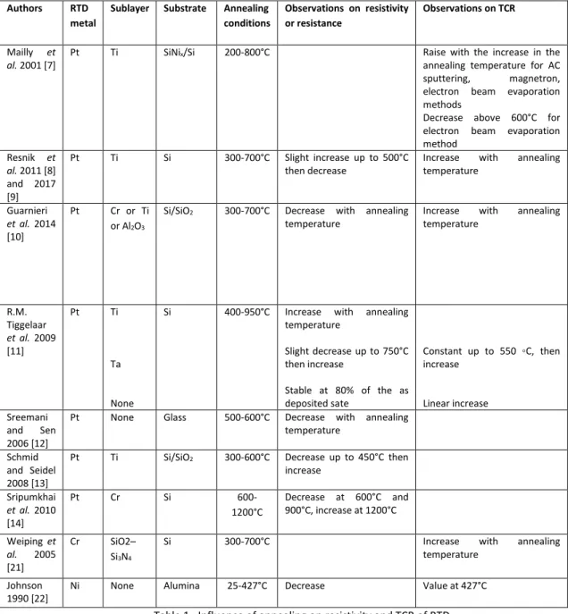
3 its TCR. Mailly et al. [7] studied a platinum thin film on a titanium sublayer for an application of anemometry. They showed that the TCR raises with the increase in the annealing temperature for all the deposition methods used. Above 600°C, the TCR was strongly reduced for the sample made from electron beam evaporation. Their results and those proposed by other authors are summarized in Table 1 where the RTD metal, sublayer, substrate, annealing temperature and observation on resistivity and TCR changes are reported. Resnik et al. [8][9] studied the design, fabrication and characterization of thin film Ti/Pt heaters and integrated temperature sensors. Thermal annealing of the deposited Ti/Pt layers was investigated revealing an increase in the resistivity up to 500°C then a decrease. They also showed an increase in the temperature coefficient of resistance (TCR) with the annealing temperature. Guarnieri et al. [10] studied the adherence of platinum thin film on a Si/SiO2 wafer using chromium, titanium or alumina as sublayer. They reported a decrease in resistivity with the annealing temperature and an increase in the TCR. Others authors only reported results on the resistivity of the platinum film. R.M. Tiggelaar et al. [11] observed that oxidation and diffusion of titanium or tantalum buffer layers into a platinum film during annealing leads to an increase in the resistivity. Sreemani and Sen [12] studied the effect of annealing temperature on the structural, electrical and microstructural properties of thin Pt films. They showed that resistivity of Pt films decreases appreciably up to 500 °C. They also showed that annealing improves the degree of crystallinity of Pt films and that micro-strain of the film decreases. Schmid and Seidel [13] studied the influence of annealing under vacuum and film thickness on the electrical resistivity of evaporated Ti/Pt thin films. They observed a diminution of the resistivity at an annealing temperature of 300°C then a raise at an annealing temperature of 450°C. Above 600 °C, they state that the diffusion of titanium into the platinum top layer and its plastic deformation dominate the electrical behaviour. Sripumkhai et al. [14] investigated the effect of annealing condition on a Cr/Pt thin film. The authors found that after annealing, the grain size of the Pt film increased and the electrical resistivity decreased remarkably. Finally, some authors focus on the microstructural changes after heat treatment and particularly on the titanium sublayer diffusion into the platinum film [15][13][16][17][18][19][20]. They showed that annealing at high temperature lead to a diffusion and oxidation of the Ti sublayer generating compressive stress. As for other metals than platinum, Weiping et al. [21] studied a chromium membrane for temperature sensing developed in the case of a polymerase chain reaction (PCR) application. Their results indicated that the TCR increases with the heat treatment temperature going up, then levels off. Johnson [22] studied the resistivity and TCR of nickel thin films (0.125 to 1.25 μm) used as interconnections on an alumina substrate. A significant decrease of about 1 Ωcm in the resistivity of nickel films was observed after annealing at 427°C primarily due to dislocation sinking. A TCR of 0.0051 C-1 was observed between 25°C and 427°C for a film thickness of 1 μm.
As a summary, annealing leads to different phenomena that happen at different conditions and temperatures: decrease in micro-strain, raise in crystallinity, diffusion and oxidation of the sublayer if any. Therefore, it is useful to gain knowledge on the influence of an annealing process on the resistivity and TCR of a nickel RTD associated with a sublayer and substrate. In this paper, we focus our work on the influence of low temperature annealing on the characteristics of a nickel RTD designed for a heat flux sensing application up to 200°C. The RTD concept, practical design and microfabrication technique are presented in the first section. In the second section, the characterization of the thin films through profilometry and Scanning Electron Microscopy (SEM) is presented. The experimental setup for the temperature and resistance measurement is detailed in the following section. Finally, experimental results for the temperature measurement without and with annealing are presented and discussed. 3 4 5 6 7 8 9 10 11 12 13 14 15 16 17 18 19 20 21 22 23 24 25 26 27 28 29 30 31 32 33 34 35 36 37 38 39 40 41 42 43 44 45 46 47 48 49 50 51 52 53 54 55 56 57 58 59 60
4
Authors RTD
metal
Sublayer Substrate Annealing conditions Observations on resistivity or resistance Observations on TCR Mailly et al. 2001 [7]
Pt Ti SiNix/Si 200-800°C Raise with the increase in the
annealing temperature for AC sputtering, magnetron, electron beam evaporation methods
Decrease above 600°C for electron beam evaporation method Resnik et al. 2011 [8] and 2017 [9] Pt Ti Si 300-700°C Slight increase up to 500°C then decrease
Increase with annealing temperature Guarnieri et al. 2014 [10] Pt Cr or Ti or Al2O3
Si/SiO2 300-700°C Decrease with annealing
temperature
Increase with annealing temperature R.M. Tiggelaar et al. 2009 [11] Pt Ti Ta None
Si 400-950°C Increase with annealing temperature Slight decrease up to 750°C then increase Stable at 80% of the as deposited sate Constant up to 550 ◦C, then increase Linear increase Sreemani and Sen 2006 [12]
Pt None Glass 500-600°C Decrease with annealing temperature
Schmid and Seidel 2008 [13]
Pt Ti Si/SiO2 300-600°C Decrease up to 450°C then
increase Sripumkhai et al. 2010 [14] Pt Cr Si 600-1200°C Decrease at 600°C and 900°C, increase at 1200°C Weiping et al. 2005 [21] Cr SiO2– Si3N4
Si 300-700°C Increase with annealing temperature
Johnson 1990 [22]
Ni None Alumina 25-427°C Decrease Value at 427°C
Table 1 : Influence of annealing on resistivity and TCR of RTD 1 Concept, design and microfabrication of the sensor
1.1 Concept
Gradient heat flux sensors are based on the application of Fourier’s law:
𝒒 = −𝝀
∆𝑻𝒆 (1)
where the temperature difference
∆𝑇
is measured across a substrate of known thickness e and conductivity𝜆
. The thermal resistance of the sensor e/λ is usually small in order to avoid disturbance of the thermal environment.The resistivity 𝜌 of thin metal film can be expressed as Matthiesen’s rule [22]: 3 4 5 6 7 8 9 10 11 12 13 14 15 16 17 18 19 20 21 22 23 24 25 26 27 28 29 30 31 32 33 34 35 36 37 38 39 40 41 42 43 44 45 46 47 48 49 50 51 52 53 54 55 56 57 58 59 60
5
𝜌 = 𝜌𝑇+ 𝜌𝑟
(2)
where 𝜌𝑇 is the temperature-dependant term and 𝜌𝑟 is the residual resistivity term. 𝜌𝑟 includes the
contribution from surface scattering, impurities, magnetic disorder effects, grain boundaries and intragranular effects. Thus, using thin film metal RTD in a gradient heat flux sensor requires that the variation of resistivity is only linked to the temperature variation and not to uncontrolled variations of the residual resistivity. If not, this variation divided by a small thermal resistance would lead to large heat flux errors.
Assuming the resistivity evolves linearly with temperature:
𝜌(𝑇) = 𝜌0(1 + α(T − T0))
(3)
where
𝜌
0is the resistivity of the material at the reference temperatureT
0.
This implies that the resistance of the RTD can be expressed as:
𝑅(𝑇) = 𝑅0[1 + 𝛼(𝑇 − 𝑇0)]
(4)
where
𝑅
0is the resistance at the reference temperatureT
0.
The TCR α can be expressed as:α = 1 𝑅0 dR 𝑑𝑇= 𝑅(𝑇)−𝑅0 𝑅0(𝑇−𝑇0)
(5) 1.2 Design
The heat flux sensor is made from two RTDs deposited on each side of a Borofloat glass substrate (Figure 1). A 20 nm sublayer made of chromium ensures the adhesion between the substrate and the nickel. The thickness of the nickel track is about 220 nm. The total sensor dimensions are 5 x 5 x 0.5 mm3, with a sensing area of 2 x 2 mm2. More details on the sensor can be found in previous works where platinum RTDs were used [23]. The properties of the materials used in the sensor are summarized in Table 2.
Figure 1 Heat flux sensor scheme (a) and photograph (b)
Property Borofloat Glass Nickel Chromium
Coefficient of linear expansion al (C-1) (20-300 °C) 3.25 x 10⁻⁶ 13.3 x 10⁻⁶ 6.5 x 10⁻⁶
Resistivity ρ (Ω.m) at 25 °C 6.9 x 10⁻⁸ 13.2 x 10⁻⁸ TCR α (C-1) at 25-500 °C (bulk) 0.0068 0.00214 Table 2 Properties Chromium Nickel 0,02 µm 0,2 µm 500 µm Borofloat 33 a/ b/ 3 4 5 6 7 8 9 10 11 12 13 14 15 16 17 18 19 20 21 22 23 24 25 26 27 28 29 30 31 32 33 34 35 36 37 38 39 40 41 42 43 44 45 46 47 48 49 50 51 52 53 54 55 56 57 58 59 60
6 1.3 Microfabrication
The RTDs for the heat flux sensor were manufactured in the MIMENTO cleanroom at FEMTO-ST institute. The wafer is a Borofloat glass wafer, 4 inches in diameter and a thickness of 500 microns. The microfabrication process follows the steps given on Figure 2. First (1) the glass wafer is coated with a thin photoresist Shipley 1813 by spin coating. The mask aligner then allows the exposure to UV of the photosensitive resin according to the mask (2). Then, after development of the photoresist in a basic developer MF26A from Shipley (3), the wafer is installed in a sputtering machine PLASSYS MP500. After an etching step with argon gas in order to remove all the impurities from the surface of the glass, the metal deposition, around 20 nm of Chromium as adhesive layer and 220 nm Nickel, is performed by magnetron sputtering at a pressure of 4x10⁻³mbar (4). Finally, the chemical lift-off removes the resin retaining only the patterns registered tracks (5). These five steps are repeated on the other side of the wafer with the same lithography mask in order to be able to measure the heat flux easily. The final step is the cutting of sensors from the wafer by a high rotating speed dicing saw DISCO DAD3321 and a special blade of 200µm thickness .
Figure 2 Microfabrication steps
1.3 Annealing
An annealing was performed during 6h in air on the sensors at four different annealing temperatures TA 150 °C, 200°C, 250°C, 300°C. The applied temperature profile is presented in Figure 3. A slope of 5°C/min is applied up to the annealing temperature TA, and at the end of the 6h, the sample is subjected to free cooling in the oven.
3 4 5 6 7 8 9 10 11 12 13 14 15 16 17 18 19 20 21 22 23 24 25 26 27 28 29 30 31 32 33 34 35 36 37 38 39 40 41 42 43 44 45 46 47 48 49 50 51 52 53 54 55 56 57 58 59 60
7
Figure 3 Annealing temperature profile
2 Characterization of the thin films
2.1 Profilometry
The thickness of the nickel tracks was measured with an accuracy of 0.1% by a TENCOR profilometer (DEKTAK 150). Two examples of profiles on either side of the substrate are shown in Figure 4. The deposition thickness was of the order of 0.220 μm and the track width is 60 μm which is in agreement with the design.
Figure 4 Profiles of the tracks deposited on each side of the substrate.
2.2 SEM
The characterization of the nickel films was also achieved by SEM after a milling step using Focused Ion Beam (FIB). The FIB process is used to control the profile of the nickel layer. The surface of the nickel film of the sensor was observed by SEM as deposited and after annealing at 200°C and 300°C. Various magnifications were used. We did not find any structural differences, either on the surface or in
cross-Annealing temperatureoC Time (min) TAoC 360 min 22 oC Slope 5oC/ min TAoC – 6h Free cooling 0 50 100 150 200 250 300 350 400 0 100 200 300 Th ic kn ess (nm ) Length (μm) Face 1 Face 2 3 4 5 6 7 8 9 10 11 12 13 14 15 16 17 18 19 20 21 22 23 24 25 26 27 28 29 30 31 32 33 34 35 36 37 38 39 40 41 42 43 44 45 46 47 48 49 50 51 52 53 54 55 56 57 58 59 60
8 section for nickel deposition as a function of different annealing temperatures (Figure 5). Grain size and nodule distribution of columnar growth hardly changes for the different temperature levels. (Figure 5). We do not notice the presence of stress scales, stress cracks due to different annealing and the edges of the thin layers remain cleanly drawn as on the original mask of the pattern. Therefore, we do not observe major differences at the surface of the films as deposited or after annealing.
Figure 5: SEM pictures of Ni/Cr films with increasing magnification a – b – c as deposited , d – e – f annealed 6h 200°C and etched by FIB, g-h-i annealed 6h 300°C
3 Experimental setup of the resistance and temperature measurement
3.1 Temperature calibration bench, uncertainties and errors
The calibration bench was composed of a portable calibration oven (550 Gemini LRI), a highly accurate Pt100 platinum reference probe (0.005 °C) and a reference thermometer (PHP 601) (Figure 6). The RTDs were placed into the oven and were measured with two precision 61/2 digits digital multimeters Keithley 2100. They were connected with the 4-wire method with constantan wires. The 10 kΩ range of the multimeter was chosen, leading to an applied current of 0.1 mA in order to minimize self-heating. Data acquisition was performed with a Labview® software. The RTDs resistance values were
d/
a/
b/
c/
e/
f/
h/
i/
g/
3 4 5 6 7 8 9 10 11 12 13 14 15 16 17 18 19 20 21 22 23 24 25 26 27 28 29 30 31 32 33 34 35 36 37 38 39 40 41 42 43 44 45 46 47 48 49 50 51 52 53 54 55 56 57 58 59 609 measured on a 20°C-120°C range. At each temperature step, 50 observations of the resistance value were made.
Figure 6 Calibration test bench.
3.2 Uncertainties and errors
The uncertainties of the resistance measurement and temperature calibration were established following the guidelines exposed in [23][24][25]. The type A uncertainties are computed with the following equation: 𝑢𝑒𝑥𝑝 = 1 √𝑛[ 1 𝑛−1∑(𝑋𝑖− 𝑋̅) 2]1/2 (6)
For type B uncertainties, we suppose that the data provided by the constructor represent a uniform distribution between the value [-a, +a]. Therefore, the uncertainty is obtained from:
𝑢 = 𝑎
√3 (7)
The total uncertainty is computed applying the law of propagation of uncertainties. Then, the expanded uncertainty considering a confidence interval of 95% is computed as:
𝑈 = 𝑘𝑢 (8)
with the coverage factor 𝑘 = 2. The expanded uncertainty is found to be 0.14°C. The details for the resistance and temperature measurement are presented in Table 3 and in Table 4 respectively.
We consider the temperature of the reference Pt100 as the reference value. Therefore, in the next paragraphs, the absolute error is the difference between this value and the values issued from the RTDs.
Sources of uncertainties Uncertainty
type Contribution (Ω)
Resistance measurement at 120°C (n=50) A 2.25x10⁻³
Digital Multimeter resolution Keithley 2100 (10KΩ range) B 2.89x10⁻³ 3 4 5 6 7 8 9 10 11 12 13 14 15 16 17 18 19 20 21 22 23 24 25 26 27 28 29 30 31 32 33 34 35 36 37 38 39 40 41 42 43 44 45 46 47 48 49 50 51 52 53 54 55 56 57 58 59 60
10
Combined uncertainty 𝑢𝑐 3.66x10⁻³
Expanded uncertainty U (k=2) 7.32x10⁻³
Table 3 Uncertainties of the resistance measurement
Sources of uncertainties Uncertainty
type Contribution (°C)
Resistance measurement at 120°C (n=50) A 2.21x10⁻³
Digital Multimeter resolution Keithley 2100 (10KΩ range) B 2.84x10⁻³
Temperature measurement at 120°C (n=50) A 1.03x10⁻³
Reference temperature probe Pt100 B 5.77x10⁻³
Thermometer PHP 601resolution B 5.77x10⁻³
Oven temperature resolution B 5.77x10⁻²
Spatial homogeneity of the oven B 6.35x10⁻³
RTD self heating (10KΩ range) B 2.89x10⁻²
Combined uncertainty 𝑢𝑐 6.55x10⁻²
Expanded uncertainty U (k=2) 0.131
Table 4 Uncertainties of the temperature measurement
4 Experimental results and discussion
4.1 Characteristics of the sensor without annealing
The initial calibration curves of the nickel RTDs R1 and R2 as deposited (without annealing) are presented in Figure 7. 3 4 5 6 7 8 9 10 11 12 13 14 15 16 17 18 19 20 21 22 23 24 25 26 27 28 29 30 31 32 33 34 35 36 37 38 39 40 41 42 43 44 45 46 47 48 49 50 51 52 53 54 55 56 57 58 59 60
11
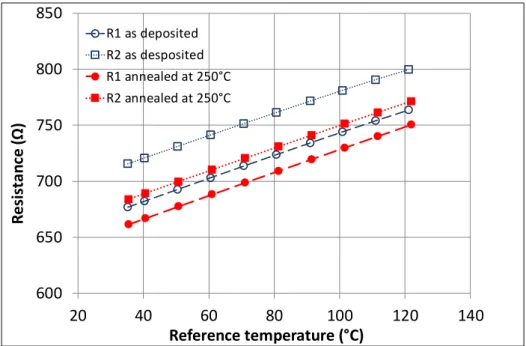
Figure 7 Calibration curves of the RTDs as deposited and with annealing at 250°C
In this temperature range, the observed variation of the resistance with temperature is close to linear. The difference in the values of resistance R1 and R2 can be explained by the difference of film deposition from one side to the other one (cf. Figure 4). The observed averaged resistivity of both resistances deduced from the track dimension was 1.31x10⁻⁷ Ω.m at 35°C and the average TCR was 0.00143 °C-1 (Table 5). As expected in thin films, we observe an increase in resistivity compared to bulk nickel (Table 2) and a decrease in TCR. As analysed by Johnson [22], the main contribution of this increase is probably due to the raise in grain boundary scattering. In order to investigate the repeatability of the measurement, several tests were performed after the calibration, and the absolute error calculated as explained in paragraph 3.2 was plotted for each reference temperature for the same sensor. The results after the 3 tests are plotted in Figure 8. It can be noticed that the resistance measurement is not repeatable enough. On the second test, the maximum absolute error strongly rose to 3°C for R1 and 4.1°C for R2. During the following tests, the error seemed to tend to a fixed value. These results suggested that the different tests achieved a partial annealing on the resistive sensors, even at low temperatures of around 100 °C. The properties of the film was modified along the tests resulting in a drift of the measurements.
TCR (°C-1)
Conditions R1 R2
As deposited 0.00149 0.00138 As deposited : average value 0.00143
After annealing 0.00156 0.00149 After annealing : average value 0.00152
Table 5 TCR as deposited and after annealing at 250°C
600 650 700 750 800 850 20 40 60 80 100 120 140 R esi st an ce (Ω ) Reference temperature (°C) R1 as deposited R2 as desposited R1 annealed at 250°C R2 annealed at 250°C 3 4 5 6 7 8 9 10 11 12 13 14 15 16 17 18 19 20 21 22 23 24 25 26 27 28 29 30 31 32 33 34 35 36 37 38 39 40 41 42 43 44 45 46 47 48 49 50 51 52 53 54 55 56 57 58 59 60
12
Figure 8 Absolute errors of the RTDs (R1 a/ – R2 b/) as deposited and with annealing at 250°C
4.2 Influence of the annealing temperature on the resistivity of the sensor
In order to overcome this problem, different annealing temperatures from 150°C to 300°C were applied (cf §1.3) to the sensor in order to determine the appropriate annealing temperature. The evolution of the resistance of the sensor versus the annealing temperature is plotted in Figure 9. We observed a decrease down to 200°C, then an increase. This phenomenon was also reported by Schmid and Seidel [13] and Zribi et al. [23] on a Pt/Ti and Pt/Cr film respectively. On the other hand, Johnson only reported a decrease in resistivity on a Ni film without sublayer. Concerning the decrease in resistance observed after annealing at the lowest temperatures, we make the hypothesis that the main contribution is linked to the release of the micro stress induced by the deposition process, as observed by Sreemani and Sen for platinum [12]. A raise in crystallinity due to the annealing can also lead to a decrease in resistivity.
Concerning the increase observed above 200°C, we make the hypothesis that the increase is due to the diffusion and oxidation of the chromium buffer layer into the nickel layer along grain boundaries, changing the electrical properties. This phenomenom was frequently observed for Pt thin films deposited on a sublayer (see for example [11]).
Figure 9 Influence of the annealing temperature on the resistance.
0 0.5 1 1.5 2 2.5 3 3.5 4 4.5 20 40 60 80 100 120 |T 1 -TREF | ( °C) Temperature (°C) Test 1 as deposited Test 2 as deposited Test 3 as deposited Test 4 annealed Test 5 annealed Test 6 annealed a/ 0 0.5 1 1.5 2 2.5 3 3.5 4 4.5 20 40 60 80 100 120 |T2 -TREF | ( °C) Temperature (°C) Test 1 as desposited Test 2 as deposited Test 3 as deposited Test 4 annealed Test 5 annealed Test 6 annealed b/ -12 -10 -8 -6 -4 -2 0 2 0 50 100 150 200 250 300 350 R esi st an ce v ar ia ti o n (% ) Annealing temperature (°C) R1 R2 3 4 5 6 7 8 9 10 11 12 13 14 15 16 17 18 19 20 21 22 23 24 25 26 27 28 29 30 31 32 33 34 35 36 37 38 39 40 41 42 43 44 45 46 47 48 49 50 51 52 53 54 55 56 57 58 59 60
13 4.3 Characteristics of the RTDs annealed at 250°C
An annealing temperature of 250°C was applied to the sensors in order to benefit from the release of stress in the film. Then, the calibration was performed using the same experimental conditions. The calibration curves of both RTDs are plotted in Figure 7. We observed a decrease in resistance, thus in resistivity. We also observed a 6% increase in the average TCR up to 0.00152 °C-1. The absolute errors versus the reference temperature are displayed in Figure 8. We observed that the annealing also led to a high improvement in the repeatability of the results. The absolute errors are reduced to a maximal error of 0.44°C instead of 4.12°C without annealing. Therefore, this choice of annealing temperature led to an improvement of the RTDs.
Conclusion
In this paper, we have presented the influence of low temperature annealing on nickel RTDs deposited on a glass substrate with a chromium sublayer. The aimed application is heat flux sensing where repeatable and accurate measurement are needed. We applied different annealing temperatures from 150°C to 300°C for 6 hours and showed that the resistivity decreased down to 200°C then increased. The films were analysed though SEM images and no major changes were observed between as deposited and annealed films. We made the hypothesis that the decrease was due to the reduction of stress in the film, and the increase was due to the oxidation and diffusion of the chromium sublayer. Applying a 250°C annealing led to repeatable temperature measurements and an increased TCR. The achieved performance seems compliant with the aimed application oh heat flux sensing.
Acknowledgements
This work has been supported by the EIPHI Graduate School (contract "ANR-17-EURE-0002") and was partly supported by the French RENATECH network and its FEMTO-ST technological facility.
References
[1] E. J. P. Santos and I. B. Vasconcelos. RTD-based smart temperature sensor: Process development and circuit design. In 2008 26th International Conference on Microelectronics, pages 333–336, May 2008.
[2] B. Davaji and C. H. Lee. A paper-based calorimetric microfluidics platform for bio-chemical sensing. Biosensors and Bioelectronics, 59:120 – 126, 2014.
[3] N. Sion. In-core moderator temperature measurement within candu reactors. Nuclear
Instruments and Methods in Physics Research, 206(3):527 – 536, 1983.
[4] M. Hayashi, A. Sakurai, and S. Aso. Investigation of a multi-layered thin film heat transfer gauge. Memoirs of the Faculty of Engineering, Kyushu University, 44(1):113–124, 1 1984.
[5] A. H. Epstein, G. R. Guenette, R. J. G. Norton, and Y. Cao. High-frequency response heat-flux gauge. Rev. Sci. Instrum., 57(4):639–649, 1986.
[6] H. Mocikat and H. Herwig. Heat transfer measurements with surface mounted foil-sensors in an active mode: a comprehensive review and a new design. Sensors, 9(4):3011–3032, 2009.
3 4 5 6 7 8 9 10 11 12 13 14 15 16 17 18 19 20 21 22 23 24 25 26 27 28 29 30 31 32 33 34 35 36 37 38 39 40 41 42 43 44 45 46 47 48 49 50 51 52 53 54 55 56 57 58 59 60
14 [7] F. Mailly, A. Giani, R. Bonnot, P. Temple-Boyer, F. Pascal-Delannoy, A. Foucaran, and A. Boyer. Anemometer with hot platinum thin film. Sensor Actuat. A: Phys., 94(1-2):32 – 38, 2001.
[8] D. Resnik, D. Vrtacenik, Pecar B. Mozek, M., and S. Amon. Experimental study of heat-treated thin film ti/pt heater and temperature sensor properties on a si microfluidic platform. Journal of
Micromechanics and Microengineering, 21(2):025025, 2011.
[9] D. Resnik, J. Kovac, D. Vrtacnik, M. Godec, B. Pecar, and M. Mozek. Microstructural and electrical properties of heat treated resistive Ti/Pt thin layers. Thin Solid Films, 639:64 – 72, 2017.
[10] V. Guarnieri, L. Biazi, R. Marchiori, and A. Lago. Platinum metallization for MEMS application.
Biomatter, 4(1):e28822, 2014. PMID: 25482415.
[11] R.M. Tiggelaar, R.G.P. Sanders, A.W. Groenland, and J.G.E. Gardeniers. Stability of thin platinum films implemented in high-temperature microdevices. Sensor Actuat. A: Phys., 152(1):39 – 47, 2009.
[12] M. Sreemany and S. Sen. Effect of substrate temperature and annealing temperature on the structural, electrical and microstructural properties of thin Pt films by rf magnetron sputtering.
Applied Surface Science, 253(5):2739 – 2746, 2006.
[13] U. Schmid and H. Seidel. Effect of high temperature annealing on the electrical performance of titanium/platinum thin films. Thin Solid Films, 516(6):898 – 906, 2008.
[14] W. Sripumkhai, S. Porntheeraphat, B. Saekow, W. Bunjongpru, S. Rahong, and J. Nukeaw. Effect of annealing temperature on platinum thin films prepared by electron beam evaporation.
Journal of the Microscopy Society of Thailand, 24(1):51–54, 2010.
[15] S.Y. Kweon, S.K. Choi, S.J. Yeom, and J.S. Roh. Platinum hillocks in Pt/Ti film stacks deposited on thermally oxidized Si substrate. Japanese Journal of Applied Physics, 40(10R):5850, 2001.
[16] W. W. Jung, S. K. Choi, S. Y. Kweon, and S. J. Yeom. Platinum (100) hillock growth in pt/ti electrode stack for srbi 2 ta 2 o 9 ferroelectric random access memory. Journal of electroceramics, 13(1-3):55–63, 2004.
[17] K. Wang, K. Yao, and S. J. Chua. Titanium diffusion and residual stress of platinum thin films on Ti/SiO2/Si substrate. Journal of Applied Physics, 98(1):013538, 2005.
[18] C.L. Dai, F.Y. Xiao, C.Y. Lee, Y.C. Cheng, P.Z. Chang, and S.H. Chang. Thermal effects in pzt: diffusion of titanium and recrystallization of platinum. Materials Science and Engineering: A, 384(1):57 – 63, 2004.
[19] H.J. Nam, D.K Choi, and W.J Lee. Formation of hillocks in pt/ti electrodes and their effects on short phenomena of pzt films deposited by reactive sputtering. Thin Solid Films, 371(1):264 – 271, 2000. 3 4 5 6 7 8 9 10 11 12 13 14 15 16 17 18 19 20 21 22 23 24 25 26 27 28 29 30 31 32 33 34 35 36 37 38 39 40 41 42 43 44 45 46 47 48 49 50 51 52 53 54 55 56 57 58 59 60
15 [20] Y.S. Jeong, H.U. Lee, S.A. Lee, J.P. Kim, H.G. Kim, S.Y Jeong, and C.R. Cho. Annealing effect of platinum-based electrodes on physical properties of pzt thin films. Current Applied Physics, 9(1):115 – 119, 2009.
[21] Y. Weiping, D. Liqun, W. Jing, M. Lingzhi, and Z. Jianbo. Simulation and experimental study of PCR chip based on silicon. Sensors and Actuators B: Chemical, 108(1):695 – 699, 2005. Proceedings of the Tenth International Meeting on Chemical Sensors.
[22] B.C. Johnson. Electrical resistivity of copper and nickel thin-film interconnections. Journal of
Applied Physics, 67(6):3018–3024, 1990.
[23] A. Zribi, M. Barthes, S. Begot, F. Lanzetta, J.Y. Rauch, and V. Moutarlier. Design, fabrication and characterization of thin film resistances for heat flux sensing application. Sensor Actuat. A: Phys., 245:26 – 39, 2016.
[24] B.N. Taylor and C.E. Kuyatt. Guidelines for evaluating and expressing the uncertainty of NIST measurement results. Technical Report TN1297, National Institute of Standards and Technology, Washington, USA, 1994.
[25] Evaluation of measurement data. Guide to the expression of uncertainty in measurement JCGM 100:2008 (GUM 1995 with minor corrections). Technical report, 1995.
3 4 5 6 7 8 9 10 11 12 13 14 15 16 17 18 19 20 21 22 23 24 25 26 27 28 29 30 31 32 33 34 35 36 37 38 39 40 41 42 43 44 45 46 47 48 49 50 51 52 53 54 55 56 57 58 59 60