Haute Ecole d'lngénierie ffl H o c h s c h u l e f û r I n g e n i e u r w i s s e n s c h a f t e n E l
Begree Ccurse Systenros
Engineerieg
ldajor: Ilrfubcnies
eâpBcma
2W33
Stép&aæwe
&æve!*p
CesbKTW
C*ç,æweæpud
æeed
fuæÊæ
fi6æve6âgewewê
Ssêewu
ffi
ffii$
.,\N
Professor C h r i s t o p h e B i a n c h i Expeft L u z i u s K r o n i gSubmissr'on date of the report 1 2 . O 7 . 2 0 ' t 3
X F S r
!
F r v
Année académique I Studienjahr 2012t13 No TD /Nr. DA ia2u3t't9 Mandant / Auftraggeber X H E S - s o V a l a i s ! I n d u s t r i e n E t a b l i s s e m e n t p a r t e n a i r e P a r t n e r i n s t i t u t i o n Etudiant I Student Stéphane Lovejoy
Lieu d'exécution / Ausftihrungsott X H E S - s o V a t a i s n I n d u s t r i e n E t a b l i s s e m e n t p a r t e n a i r e P a r t n e r i n s t i t u t i o n Professeur/ Dozent Ghristophe Bianchi
Travail confidentiel I verlrauliche Arbeit n o u i / j a t X n o n / n e i n
Experl / Experte gonnées complètes) Luzius Kronig
E P F L I A A c T S - c E I r l o t o I S t a t i o n 1 1 I 1 0 1 5 L a u s a n n e
Titre / Titel
C U b E T H C o m m a n d D a t a a n d M a n a g e m e n t S y s t e m Description et Objectifs / Beschreibung und Ziele
The Swiss Space Center is involved in a new CubeSat program called CubETH, whose goal is to fly four GNSS (Global Navigation Satellite System) sensors on a cubesat. The GNSS sensors will be used for orbit determination and if possible also for attitude determination. The Geodesy and Geodynamics lab of the ETHZ is responsible for the payload. EPFL is responsible for the platform.
The goal of the Bachelor Thesis is to contribute to the development of the CDMS breadboard. The tasks to realize are:
Review of the existing CDMS design
Design and development of the electronics of the magnetic torquer
Design and development of the electronics for the read-out of the sun sensors
Integration of theses electronics with the FPGA CDMS board already used during the semester project Propose a demonstrator to control the magnetic torquer from the sun sensors.
Signature ou visa I Unterschift oder Visum Resp. de la filière
Leiter des Studieng.: '
EtudianUStudent:
Délais / Termine
Attribution du thème I Ausgabe des Auftrags: 1 3 . 0 5 . 2 0 1 3
Remise du rapport I Abgabe des Sch/ussberichts: 12.07.2013
Expositions I Ausstellungen Diplomarbeiten: 2 8 - 3 0 . 0 8 . 2 0 1 3
Défense orale I Mtindliche Veffechtung: Semaine I Woche 36
'
Par sa signature, I'étudiant-e s'engage à respecter stictement le caractère confidentie! du travail de diplôme qui lui est confié et des informations mises â sa dlsposffion.
Durch seine Unterschrift veryflichtet sich der Student, die Veftraulichkeit der Diplomarbeit und der dafûr zur Verfûgung gestellten Informationen zu wahren.
Objectives
The goal of this Bachelor Thesis is to design a new board based on an FPGA to study the feasibility of this type of architecture for the attitude determination of a microsatellite.
Methods | Experiences | Results
This board will contribute to the development of the CubETH’s board whose goal is to fly four GNSS sensors on a CubeSat. It commands a Magnetotorquer according to a vector indicating the direction of the sun from the satellite, based on the values returned by a Sun Sensor.
The board implements all the necessary electronics for the proper operation of the Magnetotorquer and of the Sun Sensor. This card has been designed and tested from scratch.
A PC application also has been created to establish a serial connection between the board and a computer. This application also computes the Satellite-Sun vector based on the values received from the Sun Sensor. It also allows the control of the Magnetotorquer by the use of a PWM with a configurable duty cycle. The application contains an additional feature that displays a virtual representation of the satellite that can orient itself based on the value of the Satellite-Sun vector previously calculated.
This architecture based on a FPGA works fine but needs further testing to be completely validated.
CubETH Command and Data Management
System
Graduate
Stéphane Lovejoy
Bachelor’s Thesis
| 2 0 1 3 |
Degree course Systems Engineering Field of application Infotronics Supervising professor Christophe Bianchi [email protected] PartnerPolytechnic School of Lausanne
Sun Sensor wire bonded on its test board.
Magnetotorquer used to actuate the microsatellite.
Degree Course Systems
Engineering
Major :Infotronics
Diploma 2013
Stéphane Lovejoy
CubETH Command and Data
Management System
Professeur Christophe Bianchi
Expert Luzius Kronig
TABLE OF CONTENTS
LIST OF ACRONYMS ... 4 1 FOREWORD ... 5 1.1 CubeSat ... 5 1.2 SwissCube ... 5 1.3 Semester project ... 62 BACHELOR’S THESIS DEFINITION ... 6
3 INTRODUCTION ... 7
4 SYSTEM DESCRIPTION ... 8
4.1 Overall description of the system ... 8
4.2 ADCS ... 9
4.3 CDMS ... 9
4.4 Sun sensors ... 9
4.4.1 Description ... 10
4.4.2 Electronics of the Sun Sensor ... 11
4.4.3 Typical output of the Sun Sensor ... 12
4.5 Magnetotorquer ... 13
4.5.1 Description ... 13
4.5.2 Characterization of the Magnetotorquer’s Impedance ... 14
4.5.3 Current probe ... 15
4.5.4 H-Bridge and filter ... 17
4.6 FPGA board ... 17
4.7 AD converter ... 17
4.7.1 Serial Interface ... 18
4.7.2 Data write operation ... 19
4.7.3 Data read operation ... 20
5 HARDWARE DEVELOPMENT ... 21
5.1 Interface board ... 21
5.1.1 Description ... 21
5.1.2 Test of the card ... 22
6 COMMUNICATION PROTOCOL ... 25
6.1 Simple communication protocol ... 25
6.1.2 AD conversion COMMAND ... 26
6.1.3 AD value transmission ... 27
6.1.4 Weak points of this protocol ... 27
6.2 Final protocol proposition ... 28
7 FPGA DEVELOPPEMENT ... 29
7.1 UART Communication Block ... 30
7.1.1 Block description ... 30
7.1.2 Simulations ... 31
7.1.3 Test at board level ... 33
7.2 Block code_decode_Trame ... 34 7.2.1 Block description ... 34 7.2.2 Simulation ... 36 7.3 PWM generator block ... 40 7.3.1 Block description ... 40 7.3.2 Simulation ... 41
7.3.3 Test at board level ... 44
7.4 AD communication block ... 46
7.4.1 Block description ... 46
7.4.2 Simulation ... 47
7.4.3 Test at board level ... 49
8 DEMONSTRATOR ... 50
8.1 UART communication application ... 51
8.1.1 Description ... 51
8.1.2 Class overview ... 52
8.1.3 Behavior of the code ... 53
8.1.4 Validation of the communication ... 55
8.1.5 Further information concerning the coding of this application ... 55
8.2 Application for the Simulation of a Cube « Cube_draw » ... 56
8.2.1 Advantages of openGL ... 56
8.2.2 Key methods overview ... 57
8.2.3 Drawing the cube ... 58
8.3 Demonstrator integration ... 62
8.3.1 Description ... 62
8.3.2 Reuse of previous applications ... 63
8.3.3 Class overview ... 63
8.3.5 Satellite-Sun vector determination algorithm ... 70
9 STUDY ON THE ISOLATION OF THE ADCS BOARD’S SENSORS AND ACTUATORS ... 72
9.1 Components to isolate ... 72
9.2 Failure analysis ... 72
9.3 Schematic proposition and test ... 73
9.4 Estimated time needed to accomplish the task ... 73
10 SYSTEM VALIDATION ... 73
10.1 Hardware validation ... 73
10.1.1 Validation of the Sun Sensor ... 73
10.1.2 Validation of the Magnetotorquer ... 73
10.1.3 Interface board ... 73
10.2 VHDL validation ... 73
10.3 Software validation ... 74
10.3.1 Acquisition of values from the Sun Sensor and the Current Probe ... 74
10.3.2 Attitude algorithm ... 74
10.3.3 Regulation algorithm ... 74
10.4 Test of the entire system ... 75
11 CONCLUSION ... 75
12 FUTURE ORIENTATION ... 76
13 BIBLIOGRAPHY ... 76
14 APPENDIX ... 77
LIST OF ACRONYMS
AD Analogic to Digital
ADCS Attitude Determination and Control System API Application programming interface
CAN Controller area network
CDMS Command and Data Management System
CRC Cyclic Redundancy Check
FPGA Field Programmable Gate Array
GNSS Global Navigation Satellite System MT MagnetoTorquer OpenGl Open Graphics Library
PWM Pulse Width Modulation
SPI Serial Peripheral Interface
SS Sun Sensor
UART Universal Asynchronous Receiver Transmitter
VHDL Hardware Description Language
1 FOREWORD
1.1 CubeSat
The CubeSat project was developed in 1999 at the California Polytechnic State University and at the Stanford University. Those two universities developed the specification of a CubeSat to allow universities worldwide to launch small satellites at reduced cost. The Cubesat must have cubic geometry, a volume of 10 cm3 and weight under 1.33 kg. [1]
Figure 1: Artist View of the SwissCube CubeSat [2]
1.2 SwissCube
SwissCube is the first fully Swiss made satellite. It follows the CubeSat standards. The goal of this mission was to give to the EPFL students the opportunity to work on a satellite. The scientific goal of the SwissCube mission was to make optical measurements of the Nightglow phenomenon Figure 2.
Figure 2 : Nightglow phenomenon [3]
1.3 Semester project
A prototype board made to pilot a microsatellite was developed during a master’s thesis project by Bastien Praplan at the HES in Sion. This board could be neither mounted nor tested. The goal of the semester project was to validate the proper functioning of this board. This board is composed of an FPGA that implements a basic architecture. This architecture allows great flexibility regarding the number and the types of peripherals that it implements.
2 BACHELOR’S THESIS DEFINITION
The Swiss Space Center is involved in a new CubeSat program called CubETH, whose goal is to fly four GNSS (Global Navigation Satellite System) sensors on a Cubesat. The GNSS sensors will be used for orbit determination and if possible also for attitude determination. This project is being developed by the ETHZ in Zurich in collaboration with the EPFL in Lausanne. The ETHZ is responsible for the payload of the mission and the EPFL is responsible for the platform. The HES-SO Valais/Wallis is working in collaboration with the l’EPFL, and therefore it will take part in the platform development.
The goal of the Bachelor’s Thesis is to contribute to the development of the CDMS board (command data and management system).
The tasks to perform are:
- Review of the existing CDMS design
- Design and development of the electronics of the Magnetotorquer
- Design and development of the electronics for the read-out of the Sun Sensors
- Integration of these electronics with the FPGA CDMS board already used during the semester project
- Propose a demonstrator to control the Magnetotorquer from the Sun Sensors
3 INTRODUCTION
The present report describes the work accomplished during the Bachelor’s thesis “CubETH Command and Data Management system”.
As explained in the previous chapters, the EPFL is currently working on a new CubeSat project that involves the design of a new platform board for the satellite.
For redundancy purposes, such as in the case of a malfunction of the ADCS board, the CDMS board would have to take over with a simple attitude determination algorithm. Therefore it would have to be capable of reading the incoming values from the different input sensors and control the different actuators of the satellite. The EPFL’s request is therefore that a study be made to determine whether, in case of malfunction of the ADCS board, it can be isolated from the different sensors and actuators so they can be accessed from and managed by the CDMS board.
In the context of this work, an ADCS/CDMS board will have to be developed. This board will be based on the FPGA board tested during the semester project. It will have to be able to handle the acquisition of the Sun Sensor’s values. It will also have to be able to control the Magnetotorquer. To perform these two tasks, the necessary electronics to make the connection with the Sun Sensor and the Magnetotoquer will have to be created from scratch.
A serial communication will have to be implemented between the ADCS/CDMS board and the computer. This communication will have to be established so the attitude determination algorithm can be initially implemented on the computer and then subsequently on the board.
As the satellite’s attitude determination algorithm will be implemented on a computer, a program that simulates the satellite’s attitude will have to be created. This simulation will show to the user a virtual version of the satellite that can be oriented in real time with the values received from a Sun Sensor.
4 SYSTEM DESCRIPTION
4.1 Overall description of the system
This chapter gives an overall explanation of the system. A more detailed description will be elaborated in further chapters. The diagram in the Figure 3 shows the different actors that take part in the design.
Figure 3 : Diagram of the system
The goal of the system is to read the values from a Sun Sensor, evaluate them to determine the position of the sun and drive a Magnetotorquer. This system is used to simulate the orientation of a satellite in a chosen direction.
This system comprises an application program that’s running on a PC as a controller. This application commands an FPGA to obtain the values of the Sun Sensor. Once these values are obtained, a computation is performed to determine the sun’s position. Then the order is given to the FPGA to drive the Magnetotorquer accordingly. A current probe is used to measure the current that is provided to the Magnetotorquer. This information is converted into a digital value and then transmitted back to the application. This principle is used to determine when the Magnetotorquer needs to be turned off accordingly to the torque provided.
This application also allows the visualization of the satellite’s attitude by making a graphical simulation of the satellite. This computer simulation orients itself according to the values received from the Sun Sensor and the current measurements done on the Magnetotorquer.
The Magnetotorquer is driven with a PWM provided by the FPGA. An H-Bridge then allows for activation of the Magnetotorquer in one way or the other.
4.2 ADCS
The ADCS (Attitude Determination and Control System) is the part of the satellite that determines its attitude. To achieve that goal, the ADCS disposes of several inputs that are used to determine its orientation in space. These include: magnetometer, gyroscope and Sun Sensors. It also commands actuators that allow the control of the satellite: Magnetotorquer, reaction wheel.
4.3 CDMS
The CDMS (Command and Data Management System) manages the command and the data of the satellite. Its main objective is to compute the incoming data produced by the satellite: orientation and status of the different sub-systems and to store them before sending them to earth.
For the CubETH mission, the CDMS board is also used as a backup system. In case of an ADCS failure, the CDMS must be able to take over the basic attitude determination of the satellite. Therefore it will have to be able to process the incoming data from the Sun Sensors and also to drive the Magnetotorquers.
4.4 Sun sensors
The Sun Sensors (SS) are used for the attitude determination of the satellite. They allow the determination of the Satellite-Sun vector by giving two angles. Each SS provides two angles indicating the orientation of the sun compared to the satellite’s face it is placed on.
Figure 4 : DTU Sun Sensor
The SSes used for CubETH are the same as were used for the SwissCube mission. These SSes were developed at the Danish Technical University. This university also used them in a previous CubeSat mission called DTUsat. Therefore these SSes have already been proven in several space missions.
4.4.1
Description
This chapter contains a basic description of the Sun Sensors. More precise information can be found in the report in bibliography [4]. This report can be found in the DVD in annex.
Figure 5 : (a) Top view of the sun sensor chip. (b) Axes of angle 1 and 2 [4]
For the determination of the two angles, (Figure 5b) six photodiodes are used. When these photodiodes are exposed to sunlight, they generate a current. This current is proportional to the illuminated surface, which depends on the incident angle of the sunlight as shown in Figure 6 (b).
(c)
Figure 6 : Top view (a) and front view (b) and Sensor dimensions (c) of one of the slits of the sensor [4]
4.4.2
Electronics of the Sun Sensor
This chapter explains a simplified version of the electronics of the SS. The complete and exact electrical schematics can be found in appendix 2. As shown in Figure 7, the circuit is a current-to-voltage converter with a gain set by R1 (a) and R2 (b).
Figure 7 : Electronics for one angle. Simplified schematic. (a) Angle detection diodes, (b) Reference diode [4]
In the part (a) of the circuit, the two photo diodes are connected head to tail. This mounting type is used to have the differential current between Dt1 and Dt2 flowing in the resistor R1. An offset of 1.25 V is added to have exclusively positive tension on the output V1. The expression of V1 can be written as follows:
1 1 2 ∗ 1
The expression of Vref1 is a simple ohm low and can be written as following:
1 2 ∗
Low pass filters R1C1 for (a) and R2C2 for (b) were added to both circuits. The constant of the low pass filters was set as explained in the report [4].
4.4.3
Typical output of the Sun Sensor
This test was performed during the “characterization and the calibration of the SS” at the EPFL in 2008 for the SwissCube mission. Further explanations and tests can be found in the report [4].
Figure 8 shows the output for the SS with the secondary angle set to 0°. The secondary angle was set to 0 because of the influence of it on the first angle. The interference between the two angles is corrected by the angle calculation algorithm, explained in chapter 8.3.5.
Figure 8: Output signals of a SS. Angle 2 fix at 0°. [4]
The accuracy of the SS is best for small angles, around 60°. Therefore the test was run for maximum angles of -60° to 60°. The output angles have to be computed as expressed in the following formula:
1,2 ,
,
, 1.25
,
4.5 Magnetotorquer
As the Sun Sensors are used to define the position of the sun, the Magnetotorquers (MT) are used as actuators to orient the satellite in space. CubETH implements 3.
Figure 9 : Magnetotorquer
The MTs used for CubETH are the same as those used in the previous SwissCube mission.
These chapters contain a basic description of the Magnetotorqer and of its related electronics. The tests and the characterization below were performed during the Magetotorquer Impedance Characterisation at the EPFL in 2008 for the SwissCube mission. Further explanations and tests can be found in the following report [5].
4.5.1
Description
The MTs are simply coils of wire which produce a magnetic field. The interaction between the natural magnetic field of the earth and the one generated by the MT produces a torque. This resultant torque is used to orient the satellite.
The following figure shows the principle of the electronic used to command the MT.
Figure 10: Principle of the MT electronics
As shown in Figure 10, an FPGA is used to generate a PWM signal. This PWM is generated on one of the two inputs of the H-Bridge. This bridge allows us to define the direction of the current that will flow in the MT. A filter is added to smooth this current. A current probe performs the measurement of the current that is actually flowing in the MT.
4.5.2
Characterization of the Magnetotorquer’s Impedance
These tests were performed during the “Magetotorquer Impedance Characterisation” work at the EPFL in 2008 for the SwissCube mission. Further explanations and tests can be found in the following report [5].
Figure 11: Magnetotorquer equivalent circuit [5]
As shown in the Figure 11, the equivalent circuit of the MT is composed of one serial resistor and of a capacitor added in parallel.
The following characteristics were measured with a spectral analyzer at ambient temperature. These measurements give the values of the equivalent circuit of the MTs.
Figure 12 : Magnetotorquer measured characteristics at ambient temperature [5]
Figure 13: Magnetotorquer measured characteristics at 32.5 [kHz] and ambient temperature [5]
4.5.3
Current probe
The current probe measures the current that flows in the MT. This current can be either positive or negative. Therefore, a system capable of measuring bidirectional current was adopted. The following figure shows the current probe that was chosen.
Figure 14: MAX4072 current probe
This device amplifies a differential voltage on a shunt resistor. An offset is added to this differential voltage and it is then displayed on the output. The gain can be set to 50 or 100 and the recommended Rsense value goes from 5 [mΩ] to 1 [Ω].
The configuration used for this design is: Rsense = 1 [Ω]
Gain = 50 (GSEL set to zero) Vref = 1.25 [V]
The following figure shows the theoretical output voltage of the current probe.
Figure 15: Theoretical output voltage of the current probe [5]
We can see that with the offset of 1.25[V], the yellow curve is always positive for a range starting at -25[mA]. This is a sufficient offset, as the current in the MT never exceeds -23.4 [mA].
4.5.4
H-Bridge and filter
The H-Bridge allows the control of the current flow direction in the MT and powers it. The PWM is generated by the FPGA and the current is amplified using the H-Bridge. The following figure shows this aforementioned schematic.
Figure 16: Magnetotorquer electronic schema
A low-pass filter is added to lower the current variation.
4.6 FPGA board
This FPGA board was developed during a master’s project by Bastien Praplan at the HES in Sion. This board is composed of an FPGA that implements a basic architecture. This architecture allows a lot of flexibility in the numbers and in the types of peripherals that can be connected to it.
This board is used to make the link between the interface board and the application program on the PC. It is used to gather the data sent by the SS and the current measured on the MT and send them to the application where they are treated. The incoming data are in the form of analogical signals. Therefore, the FPGA board also implements an A/D converter that allows the digitalization of this data. This board also treats the actuation data for the MT and generates the corresponding PWM.
Further information on the FPGA board can be found in report “Cart processeur pour satellite” that can be found on DVD in annex and the rapport “Satellite navigation with GPS” that can be found in appendix 1.
4.7 AD converter
The AD converter used for this system is an ADS8028 from Texas Instrument. It is a 12 bit resolution converter with 8 conversion channels. The communication with the AD converter is made with an SPI bus. As a mistake was made initially during the semester project, the communication between the AD converter and the FPGA will be re-explained in the following chapter.
4.7.1
Serial Interface
The Figure 17 shows the detailed serial interface timing diagram for the ADS8028. The device used a serial clock (SCLK) for internal conversion and for data transfer into and out of the device.
Figure 17: Serial interface timing diagram [6]
The CS signal defines one frame of conversion and serial transfer. The sequence of 16 SCLK is used for conversion and data transfer. For a valid read or write operation to the AD converter, 16 clocks must be provided on the SCLK pin between the CS falling and its rising edge.
Several modes of operation can be selected by programming the control register of the AD. For this application the single channel, one conversion mode is selected and will therefore be explained. The following figure shows the sequence that has to be applied to the converter to configure its control register and to read data from it. [6]
Figure 18: Configuring a conversion and read converted value from ADS8028. One channel selected for conversion, no repeat. [6]
A valid write operation must be executed on the control register to select the desired channel. The selected channel is converted in the second frame and the conversion result can be clocked out in the third frame. During the second frame, the control register can be written to select another (or the same) conversion channel, as shown in the Figure 18. [6]
4.7.2
Data write operation
The control register configures the ADS8028 for the next conversion cycle. To configure the control register, a valid sequence of 16 bits has to be performed. The following figure shows the bit functions of the control register.
Figure 19: Control register bit function [6]
For this system, the following configuration was chosen:
Figure 20: Configuration of the control register
As shown in the figure above, the reference source selection has been set to external. Further information on this choice can be found in the appendix 3. The temperature sensor is disabled and the normal mode is selected.
4.7.3
Data read operation
The following figure shows the ADS8028 channel address bits.
Figure 21: Channel address bits [6]
As shown in Figure 17, the four first bits of the data frame specify the channel selected for conversion. The other 12 bits contain the conversion result for the selected channel.
The read operation is made as shown in Figure 18, two frames after the configuration frame. It is also clocked by the SCLK pin in the sequence of 16 clocks.
5 HARDWARE DEVELOPMENT
5.1 Interface board
In order to make the electronic link between the Sun Sensor, the Magnetotorquer and the FPGA board, it was necessary to create an interface board. The board was designed to provide the necessary electronics for proper functioning of an SS and an MT, such as a driver and a power supply.
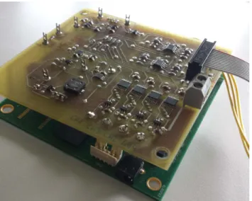
Figure 22: Picture of the Interface and FPGA board
On the figure above, one can see the interface board (yellow board) and the FPGA board (green board).
5.1.1
Description
This chapter explains the process that was followed to develop the interface board. Board specifications:
For this Bachelor’s Project the EPFL has provided only one SS and one MT. Therefore, the interface board was designed for one SS and one MT.
The different functions of the interface board are listed below: - Provide the necessary power supplies for the MT and the SS.
- Convert in tension, amplify and filter the current emitted by the photodiodesof the SS. - Implement the necessary electronics to drive the MT.
- Measure the current given to the MT when it is driven.
Schematics:
The different schematics were provided by the EPFL. They can be found in the DVD in annex. These schematics were not modified and the same components were used to provide a second validation of the design.
The interface board was initially designed for 6 SS and 3 MT (the number of SS and MT used for the satellite CubETH). However for reasons of time and complexity of routing, it was decided to make an interface for a unique SS and MT.
Schematics on PCad :
The schematic was created with PCad 2006.
In order to protect the more sensitive analogical signal, it was decided to completely separate the analogical and digital power supplies. Therefore, the two different worlds have their own DC/DC converters. The ground planes were also completely separated. There is only one single connection point. All the schematics can be found in appendix 2.
5.1.2
Test of the card
Test of the schematic of the board
All the power sources of the board were tested. The measured values are shown is appendix 4. A control was also performed that showed that all complex components on the board were correctly powered and correctly connected together. This test can be seen in appendix 5.
These two tests validate that all the components are correctly powered and correctly linked together according to the schematic of the board “Interface FPGA to Sun sens/Mag Torquer, V1.0” that can be found in appendix 2.
Test of the current probe MAX4072
As per chapter 4.5.3, the current’s value flowing in the MT was measured for various values of the PWM duty cycle at a frequency of 200 [kHz].
The following figure shows the practical output voltage of the current probe.
Figure 23: Practical output voltage of the current probe
As we can see on the figure above, the positive values are as expected. Unfortunately the negative measure doesn’t worf. No explanation for this behavior has yet been found. The problem could come from either the current probe or the H-bridge. No other component could influence this behavior.
The complete test of the current probe can be found in appendix 3.
0 0.25 0.5 0.75 1 1.25 1.5 1.75 2 2.25 2.5 2.75 3 0 1 2 3 4 5 6 7 8 9 10 11 12 13 14 15 16 17 18 19 20 21 22 23 24 Output of the current probe [V] Measured Current [mA]
Current probe measure
CurrentTest of the Sun Sensor’s electronics
The output values of the SS were measured on PT_SS_S1, PT_SS_R1, PT_SS_S2 and PT_SS_R2 according to the schematic of the board “Interface FPGA to Sun sens/Mag Torquer, V1.0” that can be found in appendix 2, for various values of irradiation. This test is presented in the figure below.
Figure 24: Measure of the SS’s outputs values
We can see on the figure above, that the measurements don’t match the intended values of Figure 8. All the reference values for R1 and R2 show higher voltage than expected. This could be modified by adapting the gain of the amplifier, as explained in chapter 4.4.2.
These measurements were taken at 1400 [W/m^2] because this is the theoretical level of irradiation in space near Earth, and at 1000 [W/m^2] because this is the irradiation level on Earth.
All those tests were performed with a halogen lamp of 1000 [W] and the irradiation was measured with a radiation meter with the following characteristics:
Brand: Kipp & Zonen Type: CC20
Serial no: CC20960168
Global validation of the interface board
Apart from the problem of the current probe, the interface board works correctly. Several minor routing mistakes were made. No second PCB was made.Tthe routing mistakes were corrected on the board. A new version of the schematic has been made which correct those mistakes. This new schematic can be found in the DVD in annex.
6 COMMUNICATION PROTOCOL
6.1 Simple communication protocol
A simple communication protocol was elaborated to manage the flow of UART frames between the application on the PC and the FPGA. Three cases within the application use this protocol. The first one is when the application on the PC asks the FPGA to generate a PWM. The second one is when the application on the PC asks the FPGA to start an AD conversion and the last one is when the FPGA sends back to the application the result of the AD conversion. These three cases in the application are explained in details below.
6.1.1
PWM generation
This case of utilization is employed when the application on the PC needs to generate a PWM to command the MT on the Interface board. The duty cycle of the PWM can be configured along with the direction of the current that flows in the MT. The following figure shows the form of the message.
Figure 25: Message to the FPGA containing the Duty Cycle of the PWM
Each frame is an individual UART frame of 8 bits of data plus the start and stop bits of the UART protocol. We can see on the Figure 25 that the first UART frame sent to the FPGA is the start frame. The second one contains the address of the PWM generator block (see chapter 7.3). As only one PWM generator block is present in the FPGA’s design, only one address has been attributed. The last frame is separated into two parts. The first one contains the value of the current’s direction that has to flow in the MT (Pos/Neg). If this value is set to one, the current will be positive and if set to zero the current generated will be negative. The second part of the last UART frame contains the value of the duty cycle that has to be generated by the block PWM_Gen of the FPGA. This value can be set from 0000000 to 1100100 (100).
6.1.2
AD conversion COMMAND
This case of utilization is emplyed when the application on the PC needs to obtain the values of the SS or the value of the current measure on the MT. The number of the AD channel on which the AD conversion will be performed is contained in the address of the AD_COM block.
Figure 26: Message to the FPGA containing the AD channel
Each frame is an individual UART frame of 8 bits of data plus the start and stop bits of the UART protocol. We can see on Figure 26 that the first UART frame sent to the FPGA is the start frame. The second one contains the channel number on which the AD conversion must be performed. A masking of the channel numbers is performed in the FPGA so all possible channel numbers are interpreted as the AD communication block address. The list of the possible AD conversion channels and their corresponding frame values can be found below.
Figure 27: List of the possible AD conversion channel
The masking is then performed on these possible UART frames with the following mask value: 0000 1111
6.1.3
AD value transmission
This case of utilization is employed when the FPGA sends back to the application on PC the value of the AD conversion. The channel on which the AD conversion was performed is sent followed by the 12 bits of the AD conversion.
Figure 28 : Message to the PC containing the result of the AD conversion and the channel it was performed on
Each frame is a separated UART frame of 8 bits of data plus the start and stop bits of the UART protocol. We can see on the Figure 28 that the first UART frame sent to the FPGA is the start frame. The second one contains the channel number on which the AD conversion was performed. The third frame of the message is constituted of padding bits and of the 4 MSBs of the AD conversion’s result. The last frame contains the 8 last bits of the 12 bits constituting the result value of the AD conversion.
6.1.4
Weak points of this protocol
This simple protocol is used for the development phase of the system. It works correctly in a non-perturbed environment. As no control of the validity of the message is made, it can be compromised in a more perturbed environment.
Another problem of this simple protocol is that it is to linked to the code that receives the message, such that the receiving device must determine the length of the data contained in the message. For example, when the FPGA receives a message addressed to the PWM generator block (see chapter 7.3), the FPGA decodes the destination address, ascertains that it is destined for the PWM generator block and therefore assumes that the data length is of one frame. The problem lies in the fact that the addressee decoding and the data length decoding are derived from the same frame and therefore from the same data, thus strongly linking the protocol to the application. This is not an issue as long as the number of addressed block stays small, but the code would become much more complicated in the event of a large number of addressed blocks.
A solution for those two problems is proposed in the following chapter.
6.2 Final protocol proposition
The simple communication protocol described in the previous chapter was used for the development phase of the system. To address the weaknesses previously mentioned, a more complete protocol is proposed.
This protocol has been inspired by the CAN protocol.
Figure 29: Proposition for the final communication protocol
The Start frame and Data could remain unchanged, but as we can see in Figure 29 the other frames would have to be modified to fit this protocol.
The Address frame contains the destination address. The destination could be a block on the FPGA, the computer or another device.
The next frame contains the length of the data in bytes that is contained in this message (it can also be equal to 0).
A CRC is added to verify whether the message has been compromised or not.
A Stop Frame could also be added, though this is not absolutely necessary, as the CRC could also act as a stop frame. The CRC could also be included in the Stop Frame.
This protocol ensures a safer way to exchange messages between the FPGA and the computer. It also has the advantage that the message’s receiver doesn’t have to decode the message’s addressee to ascertain the data length. Those two tasks could therefore be separated to reduce the complexity of the code.
7 FPGA DEVELOPPEMENT
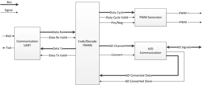
This chapter describes the different VHDL blocks that are implemented to drive the MT and to read the values from the SS from the FPGA board. The diagram in Figure 30 shows the organization of the different blocks.
Figure 30 : Diagram of the VHDL interface code
A first block performs the parallelization of the serial data transmitted by the application on the PC. Once these data are parallelized, a second block decodes the UART frames and extracts the useful information. This information is comprised of:
The destination of the frame. The frame can be addressed to the PWM block or to the A/D communication block.
The duty cycle. If the frame is addressed to the PWM block, it contains the duty cycle of the PWM that must be generated by this block. It also determines on which output the PWM is generated.
The Channel of the A/D conversion. If the frame is addressed to the A/D communication block, it contains the number of the channel on which the A/D conversion must be done. The PWM Generator block generates a PWM at a fixed frequency and at a variable duty cycle. The duty cycle can be modified at any time, however the PWM’s frequency must be defined prior to the synthesizing of the VHDL code.
The A/D communication block commands the AD converter. It defines on which channel the conversion will be done. It also provides the necessary signals used to configure and perform the conversion.
7.1 UART Communication Block
This block allows the parallelization of the incoming UART frame and the serialization of the outgoing frame.
7.1.1 Block description
This block allows the parallelization of the incoming UART frames. It also serializes the outgoing frames and clocks the UART communication.
Figure 31 (a) shows the graphical representation of the block with its generic parameters and their default values. Figure 31 (b) shows its signal table.
Figure 31 : uartCom bloc. (a) Symbol. (b) Signals table
Baud Rate :
The generic parameter baudRateDivide defines the baud rate of the UART communication. This parameter is redefined to take into account the FPGAs clock frequency, using the following formula:
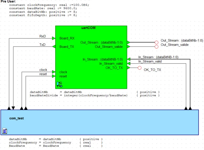
The actual configuration is used for the redefinition of the generic parameter baudeRateDivide: clockFrequcy : real := 100.0E6
baudeRate : real := 9600.0 Incoming frames:
The serial frames enter on the input Board_RX. The block automatically defines the start of the frame. Once the frame has been received, it is parallelized. When this operation is done, the frame is put on the output Out_Stream. To indicate when the frame is valid, the output Out_Stream_valid is passed to high level.
Outgoing frames:
The output OK_TO_TX allows the block to indicate when it is ready to receive new frames that need to be sent on the UART bus. This parallel frame has to be put on the input In_Stream. The input In_Stream_valid has to be set at high level to indicate that the frame is valid. Once this step is done, the frame is serialized and sent on the UART bus.
7.1.2 Simulations
To confirm that the block is working correctly, a simulation was performed. It allows one to show the behavior of the block when an UART frame is received and sent.
Test setup:
The following figure shows the schematic and the values of the parameters that were used to perform this simulation.
Figure 32 : Schematic of the UART communications simulation
Results of the simulation:
The Figure 33 shows the results of the simulation of the reception of an UART frame.
The following data is sent on the input RxD (MSB to LSB): 0111011. The frame is wrapped with a start bit of value 0 and a stop bit of value 1. The data are sent in little endian format (LSB first).
When the 8th bit is received, the output Out_Stream_valid is passed to high level for one clock period. At this moment, the output Out_Stream takes the value of the serial frame. The UART frame is correctly received in LSB first format, the start and stop bits are correctly at 0 and 1.
Figure 33 : Result of the simulation of the reception of an UART frame
Figure 34 shows a zoom of the figure above. It shows with greater precision what is going on when Out_Stream_valide is set to high level.
Figure 34 : Zoom of Figure 33
Out_Stream_valid is correctly passed at high level for one clock period. We also note that Out_Stream takes the value of the received serial frame on RxD.
Figure 35 shows the result of the simulation of the transmission of a serial frame on the UART bus.
Figure 35 : Result of the simulation of the transmission of an UART frame.
The parallel data is sent on the input In_Stream: 01101111. We can see that the UART frame sent on TxD has the desired value. We can also note that In_Stream_valid is set to high level, prior to the transmission of the frame for on clock period. This step allows us to validate the value of the frame that has to be sent.
The Figure 36 shows a zoom of the figure above. It shows with greater precision what is going on when In_Stream_valide is set to high level.
Figure 36 : Zoom of the Figure 35
Several different values are sent on the input In_Stream. The serial frame on TxD matches the data on In_Stream when In_Stream_valid is set at high level. In this case, it correctly corresponds to the desired value of 01101111.
Once the fame is validated by In_Stream_valid, the output OK_TO_TX is set at high level to indicate that the block is ready to receive new data.
The result of these two simulations shows that the different signals behave as expected. It therefore allows to synthesize this VHDL block and perform further tests on the FPGA board.
7.1.3 Test at board level
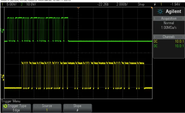
An oscilloscope measurement was made directly on the wire to visualize the passing UART frame. Results of the test:
The following figure shows an oscilloscope screen capture of several UART frames sent by the computer and several frames sent by the FPGA.
As can be seen in the above figure, frames are emitted by the computer (green trace) and received on it (yellow trace). As the decoding of these frames would have been fairly difficult in the context of this project, it was not performed. This test only validates that UART frames are emitted from the PC and from the FPGA. The correctness of these UART frames was only observed in chapter 8.1.1 when a string is sent to the FPGA board and received unchanged on the computer.
7.2 Block code_decode_Trame
7.2.1
Block description
Block_code_decode_Trame is the decision-making block of the system. It allows the extraction of the data contained in a UART frame. In function of the data received, it commands either the PWM block or the AD communication block. It also allows coding the AD conversions result into several UART frames. In order to communicate with the application on the PC, a simple communication protocol was developed. This protocol is described in chapter 6.1.
This block detects the start frame of the protocol and determines the number of following UART frames attached to this message. It then treats the received data to determine if they are addressed to the PWM generator block PWM_GEN or to the AD communication block adCOM.
Figure 38 (a) shows the graphical representation of the block with its generic parameters and their default values. Figure 38 (b) shows its signal table.
Figure 38 : Code_Decode_Trame block. (a) Symbol. (b) Signals table
Inputs / outputs description:
The inputs/outputs In_Stream, In_Stream_valid, Out_Stream, Out_Stream_valid and OK_TO_TX allow us to communicate with the block uartCOM to transmit and receive data in the form of UART frames.
The output PWM_Duty_Cycle allows sending the duty cycle value that the block PWM_GEN will have to generate. For example if the value 50 is put on this output, the PWM generated by the block PWM_GEN will have a duty cycle of 50% (It is not possible to modify the frequency of the generated PWM). The output PWM_DC_valid defines when the duty cycle on PWM_Duty_Cycle is valid. PWM_pos_neg defines the direction of the current in the MT by controlling the H-bridge.
AD_Channel defines the channel on which the AD conversion will be performed. The signal AD_Convert_valide validates the channel and gives the order to the block adCOM to start the AD conversion. The input AD_Converted_Data contains the result of the AD conversion and AD_Convert_done indicates when this value is valid.
E_AVCC enables the power supply for the analogical component of the interface board. E_SS activates the power supply for the SS and its related electronics. SS_MUX_A0…2 are the control signals of the multiplexer. These signals select which SS will be converted by the AD converter. For this bachelor’s thesis, only one SS is used, therefore these outputs are always set at low level. E_SS_MUX enables the multiplexer.
The following state machine defines the behavior of this block:
Figure 39: state machine of Code_Decode_Trame block
7.2.2
Simulation
To validate the proper operation of this block, a simulation was developed. It validates the proper behavior of the state machine (Figure 39). It also shows the behavior of the block when it receives frames form the block uartCOM. Finally, it shows that the blocks PWM_GEN and adCOM are properly controlled.
Test setup:
The figure below shows the schematic and the values of the parameters which were used to performed the simulation of the block Code_Decode_Trame.
Results of the simulation:
The following figure simulates the control of the block PWM_GEN by the block Code_Decode _Trame.
Figure 41 : Result of the simulation. Section control of the block PWM_GEN: positive current and 70% of duty cycle
Figure 41 shows the decoding of the communication protocol (described in chapter 6.1) by the block Code_Decode_Trame. The protocol frames are correctly received on the input in_stream and correctly validated by in_stream_valid. This test was set so that this block would have to command the PWM_GEN block so that it generates a PWM with a duty cycle of 70% and so that the current engendered by the PWM is positive.
Following the state machine of the block Code_Decode_Trame at Figure 39, we can see that when the start frame is received, the state machine jumps to the state Decode Address. As the received address corresponds to a PWM_GEN address (10000000) the state machine jumps to the state Set PWM duty cycle. In this last state the data frame is decoded. The MSB is used to define if the current must be positive or negative. In this case it is at 1, so the current must be positive. The next seven bits are used to define the duty cycle of the PWM. In this case they are at 70 (1000110). We can see that when pwm_dc_valid is set at high level, the output pwm_duty_cycle corresponds to 70 (1000110) and pwm_pos_neg is set at 1.
The following figure simulates the control of the block PWM_GEN by the block Code_Decode _Trame.
Figure 42 : Result of the simulation. Section control of the block PWM_GEN: negative current and 50% of duty cycle
Figure 42 shows the decoding of the communication protocol (described in chapter 6.1) by the block Code_Decode_Trame. This test is the same as the previous one except that the parameters of the PWM which have to be generated by the block PWM_GEN have been modified to: Duty Cycle 50% and negative current.
As the decoding approach is the same as the previous test, it will not be re-explained here.
We can see that the output pwm_duty_cycle has the expected value of 50(00110010) and that pwm_pos_neg is correctly set to 0 when the signal pwm_dc_valid is set to high level.
These two simulations confirm that the block Code_Decode_Trame correctly commands the block PWM_GEN.
The following figure simulates the control of the block adCOM by the block Code_Decode_Trame.
Figure 43 : Result of the simulation. Section control of the block adCOM. AD conversion on channel 1
The Figure 43 shows the decoding of the communication protocol (described in chapter 6.1) by the block Code_Decode_Trame. The protocol’s frames are correctly received on the input in_stream and correctly validated by in_stream_valid. This test was set so that this block would have to command the adCOM block so that it starts an AD conversion on the channel 1.
Following the state machine of the block Code_Decode_Trame in Figure 39, we can see that when the start frame is received, the state machine jumps to the state Decode Address. As the received address corresponds to an adCOM address (00000001) the states machine saves the 4 LSBs of the frame and jumps to the state Start AD conversion.
In this state, the 4 bits previously saved are used to define on which port the AD conversion must be done. In this case the channel 1 is selected (0001). This value is then put on the output ad_channel and the command to start the AD conversion is sent to the block adCOM by setting the ad_convert output to high level. The data on ad_channel are only valid during the time ad_convert is at high level. Then the state machine goes to the state Wait AD conversion done. In this state, the state machine waits until the AD conversion has been completed. When the signal AD_Convert_done indicating that
the AD conversion is done passes to high level, the data on ad_converted_data are saved. In this case they are 111110101010.
The state machine then jumps to the last state Send response. In this state the answer message is created. Figure 44 is a zoom of Figure 43 of the part where the answer message is created. The answer message follows the same communication protocol as explained in chapter 6.1. The start frame is sent first (10101010) on out_stream and validated by out_stream_valid then the AD channel on which the AD conversion was performed is sent (00000001). The third frame contains 4 padding bits followed by the 4 MSBs of the AD conversion (00001111). The last frame contains the 8 LSBs of the AD conversion (10101010).
Figure 44 : Zoom of the Figure 43
This simulation confirms that the block Code_Decode_Trame correctly commands the block adCOM. No board level tests were performed on this block. The correct results were observed through the tests at board level made on the other blocks, as this block commands the others, we can deduce that it is working correctly.
7.3 PWM generator block
7.3.1
Block description
This block is used to generate a PWM with a controllable duty cycle. The PWM can be emitted on one of the two different outputs. This mechanism is used to control the current direction in the MT by using an H bridge.
Figure 45 (a) shows the graphical representation of the block with its generic parameters and their default values. Figure 45 (b) shows its signal table.
Figure 45 : bloc PWM_GEN. (a) Symbol. (b) Signal table
Clock frequency and PWM frequency:
The generic parameter frequencyDivide allows the generation of a PWM with a defined frequency regardless of the clock frequency of the system, using the following formula:
The actual configuration is used for the redefinition of the generic parameter baudeRateDivide: clockFrequcy : real := 100.0E6
PWMFrequency : real := 200.0E3
The frequency of the generated PWM is set prior to synthesizing. Therefore it cannot be modified after this operation.
Inputs outputs description:
The desired duty cycle is applied on the input Duty_Cycle. It can be set with a precision of 1%. The input Duty_Cycle_valid defines when the duty cycle applied on Duty_Cycle is valid.
The input Pos_Neg defines on which output (PWM_pos or PWM_neg) the PWM will be generated. PWM_pos and PWM_neg are the two outputs on which the PWM will be generated. The PWM can only be generated on one of these two outputs at one time.
Output E_MT enables the power supply for the MT and for it related electronics. This output is set at high level when a PWM with a duty cycle different than 0% is generated.
7.3.2
Simulation
To validate the proper operation of this block, a simulation was developed. It validates the behavior of this block when different duty cycles are applied on the input Duty_Cycle. It shows that the PWM is
generated with the proper frequency, duty cycle and on the proper output. Finally it shows that the output E_MT is correctly controlled.
Test setup:
The figure below shows the schematic and the values of the parameters which were used to performed the simulation of the block PWM_GEN.
Figure 46 : Schematic of the block PWM_GEN
The parameter clockFrequency is defined to 100 M to match the FPGAs board clock frequency of 100 [MHz].
PWMFrequency is set to 200 [kHz].
The calculation of the parameter frequencyDivide is made during the synthesizing. That is why the parameters clockFrequency and PWMFrequency can be set to such high values.
Simulation results:
Figure 47 shows the simulation result of the generation of a PWM one the output PWM_pos. The duty cycle was defined to 20% and the frequency was set to 200 [kHz].
The time between the Cursor 2 and the Cursor 4 of the figure above is 5000 [ns] = 200 [kHz]. This result confirms that the PWM can be set to the desired frequency. The time between the Cursor 3 and the Cursor 4 is 1000 [ns]. This value corresponds to the desired duty cycle of 20%.
The input value of the duty cycle is first set to 20, then to 70. The duty cycle is correctly chosen when the input Duty_Cycle_valid is at high level, setting the output PWM duty cycle to 20% as expected. When Duty_Cycle_valid is at high level, the output port for the PWM is also correctly determined with the input Pos_Neg. The effect of this validation can be seen in the figure above by noting that the PWM is generated on the correct output PWM_pos.
The output E_MT is correctly set at high level, when the duty cycle is different than 0%.
Figure 48 shows the result of a second simulation. The PWM is generated on the output PWM_neg. The duty cycle was defined to 55% and the frequency was set to 200 [kHz].
This second test was performed to validate that a PWM of a precision of 1% could be generated and to validate that it could be generated on the second output.
Figure 48 : PWM_test. Duty Cycle = 55%. Freq PWM = 200 kHz. Out neg
This simulation shows that the behavior of the block is correct. The PWM’s frequency is correctly set to 200 [kHz] (5000 ns between cursor 2 and 4). The duty cycle is 55% (2750 ns between cursor 3 and 4) and the output is correctly generated on the output PWM_neg.
Figure 49 shows the last test needed to be performed in order to validate this block. It was performed to see if the output E_MT is set to low level when a duty cycle of 0% is validated by Duty_Cycle_valid.
Figure 49 : PWM_test. Duty Cycle = 0%.
The figure above shows that the output E_MT behaves as expected. It is not set at high level when the duty cycle is validated by Duty_Cycle_valid.
7.3.3 Test at board level
A test was performed at board level to determine if the PWM is generated with the designed duty cycle and the correct frequency, on the desired input of the H-bridge.
Result of the test:
The following figure shows an oscilloscope screen capture of a PWM generated on the input PWM+ of the H-Bridge (see Figure 16).
Figure 50: Oscilloscope screen capture of the PWM generated on the PWM+ input of the H-Bridge
For this first test, a PWM with the following characteristics was generated by the block PWMgen of the FPGA:
PWM frequency = 200 [kHz]
Duty Cycle = 50% => positive current flowing in the MT
Figure 50 shows that the generated PWM’s frequency and duty cycle are correct. As the measurement was performed on the input PWM+ of the H-Bridge, it indicates that the current that flows in the MT is positive.
The following figure shows an oscilloscope screen capture of a PWM generated on the input PWM- of the H-Bridge (see Figure 16).
Figure 51: Oscilloscope screen capture of the PWM generated on the PWM- input of the H-Bridge
For this first test, a PWM with the following characteristics was generated by the block PWMgen of the FPGA:
PWM frequency = 200 [kHz]
Duty Cycle = -20% => negative current flowing in the MT
Figure 50 shows that the generated PWM’s frequency and duty cycle are correct. As the measurement was performed on the input PWM- of the H-Bridge, it indicates that the current that flows in the MT is negative.
These two tests validate the correct operation of the block PWMgen.
7.4 AD communication block
7.4.1
Block description
This block is used to control and configure the AD converter. It establishes an SPI communication with the converter and sets its configuration register.
The Figure 52 (a) shows the graphical representation of the block with its generic parameters and their default values. Figure 52 (b) shows its signal table.
Figure 52 : block adCOM. (a) symbol. (b) signal list
The generic parameter adDataNbBit is the AD conversion number of bits and adNbBit is the number of bits needed to configure the AD converter’s internal register.
Inputs outputs description:
The input Channel defines on which channel of the AD converter the operation will be performed on the next AD conversion.
Cmd_Convert validates the channel on which the AD conversion will be done and starts the AD conversion.
The input and output AD_MOSI and AD_MISO are the two data lines of the full-duplex SPI data bus. AD_sClk is the clock of the SPI communication that has to be generated by the master of the bus. AD_CS is the chip select signal to enable the AD converter. The output AD_PD_RST allows to reset the AD converter and AD_Busy indicates when it is busy and cannot be configured.
The output AD_Convet_done indicates when the AD conversion is done and converted_Data gives the result of this conversion.
7.4.2 Simulation
To validate the proper operation of this block, a simulation was developed. It validates the behavior of this block when the AD converter has to be configured to perform an AD conversion on the port determined by the input address. It shows that the SPI frame to configure the AD register is correctly sent and that the different control signals are properly controlled.
Test setup:
The figure below shows the schematic and the values of the parameters which were used to performed the simulation of the block adCOM.
Results of the simulation:
Figure 54 shows the simulation result of the configuration of the AD converter and the transmission of the AD conversion return value to the block Code_Decode_Trame.
Figure 54: Result of the simulation of the block adCOM
We can see that the conversion channel is 0 (address = 0000). When convert is passed to high level, the conversion is started and ad_cs is passed to low level. The frame is sent on ad_mosi to configure the AD converter register as explained in the chapter 4.7. The 15th bit enables the conversion,
the 13th sets the conversion on the channel 0 and the bit number two defines an external power source as
the reference for the conversion. Once the transmission of this frame is done, the signal ad_cs is set to high level to indicate the end of the frame.
Then the data are received on the ad_miso during the next 15 ad_sclk periods. In this test no data are sent on the ad_miso input, but we can see that the ad_cs signal is correctly set at low level at the beginning of the 15 ad_sclk periods and put back a high level at the end.
As the AD conversion response contains the channel number on which it was performed, a comparison is made to determine if the received AD conversion was performed on the correct channel. In this case as no data were received on ad_miso, no valid channel is detected and an error frame of 1010101010101010 is sent on the output ad_convert_data.
The signal ad_convert_done is then set to high level to indicate that the value on ad_convet_data is valid.
This simulation does not fully validate this block as no data are received on as_miso and because the effects of the configuration of the AD converter are not visible. These validations are performed in the following chapter.
7.4.3 Test at board level
A test was performed at board level to determine if the AD’s internal register is correctly configured, and whether the measurement is made on the correct AD channel and returned to the FPGA.
Results of the test:
The following figure shows an oscilloscope screen capture of an AD’s configuration frame.
Figure 55: Oscilloscope frame capture of the AD’s configuration frame
Yellow trace: SCLK measured on the pin of the AD converter
Green trace: configuration frame measured on the MOSI pin of the AD converter
As explained in chapter 4.7.2 the figure above shows the AD’s configuration frame. This frame is formed so the next AD conversion will be performed on the channel 2 and that it uses an external power source as reference for this conversion. This figure also shows that the configuration frame is correctly clocked by SCLK.
The following figure shows an oscilloscope screen capture of the result of an AD conversion.
Figure 56: Oscilloscope frame capture of the AD’s configuration frame
Yellow trace: SCLK measured on the pin of the AD converter
Green trace: result of the AD conversion measured on the MISO pin of the AD converter
As explained in chapter 4.7.3, the figure above shows the result of the AD conversion. It shows that the conversion was performed on the channel 2 of the AD converter. The converted value corresponds to 000000011010.
This tests shows that the AD converter can be correctly configured and that an AD conversion can be performed on the desired channel.
8 DEMONSTRATOR
The goal of this demonstration application is to read the values of an SS sent by the FPGA board. Once these values are received, a calculation determines the position of the sun relative to the orientation of the SS. Depending on the orientation of the SS, the MT will be driven to orient a virtual satellite.
To reduce the coding difficulty of the final application, different intermediary applications were designed. The first one was designed to establish an UART communication between the application and the FPGA board. The second one draws a 3D cube that can be orientated.
The different applications were designed on QT 4.8.4 and written in C++.
8.1 UART communication application
The goal of this test application is to establish an UART communication between the computer and the FPGA board. The connection is made with an RS-232 cable using the UART protocol. The complete code of this application can be found in the DVD in annex.
8.1.1 Description
This application allows the sending of a character string to the FPGA board.
Figure 57 : UART communication application
Once the character string has been parsed into several UART frames, these are sent to the FPGA. For this test, the FPGA is configured to return without modification the received frames to the computer. The application decodes the received UART frames and displays them. The Figure 57 shows a frame exchange. On this figure we can verify that a character string is entered in the field Send and that the identical string is displayed in the field Receive.
8.1.2 Class overview
The Figure 58 shows the different classes that take part in the design of the application UARTcom.
Figure 58: UARTcom class diagram
The class Intelligence is the decision-making class of the design. It creates the instance of the classes COM, QextSerialEnumerator and GUI. All the decoding of the frames and the forming of the UART frames is done in this class.
The class COM creates the instance of the class QextSerialPort. It contains the methods that allow the communication on the serial port by calling the methods from QextSerialPort.
The class GUI displays the graphical user interface on the screen.
The classes QextSerialEnumerator and QextSerialPort are two API classes used to communicate on the serial port.
8.1.3
Behavior of the code
This chapter gives a description on the behavior of the code. Creation of a new connection:
The following figure show the behavior of the code when a new connection is opened.
Figure 59: Sequence diagram of the opening of a new connection
When the code starts, all the available ports are scanned by the instance ports of the class QextSerialEnumerator. They are then displayed on the graphical user interface. When the user has chosen a port, clicked on the button connect and then start (see Figure 57), the object intell creates the object com that itself creates the object port to open a new serial communication. The settings of the UART communication are done in the constructor of the class COM.
Transmission of an UART frame:
The following figure show the behavior of the code when a text is entered and is sent on the UART bus.
Figure 60: Sequence diagram of the transmission of an UART frame
When the user enters a text in the cell send (see Figure 57), the text is captured by the method textentered() of the class GUI and sent to the class Intelligence where it is separated into frames of 8 bits. Once the text has been parsed, it is send to the class QextSerialPort where it is then sent on the UART bus.
![Figure 6 : Top view (a) and front view (b) and Sensor dimensions (c) of one of the slits of the sensor [4]](https://thumb-eu.123doks.com/thumbv2/123doknet/15024310.684600/14.892.259.657.659.1096/figure-view-view-b-sensor-dimensions-slits-sensor.webp)
![Figure 7 : Electronics for one angle. Simplified schematic. (a) Angle detection diodes, (b) Reference diode [4]](https://thumb-eu.123doks.com/thumbv2/123doknet/15024310.684600/15.892.266.644.281.600/figure-electronics-simplified-schematic-angle-detection-diodes-reference.webp)
![Figure 15: Theoretical output voltage of the current probe [5]](https://thumb-eu.123doks.com/thumbv2/123doknet/15024310.684600/20.892.118.792.173.684/figure-theoretical-output-voltage-current-probe.webp)