Everest Wang Huang
S.B., Massachusetts Institute of Technology (1996)
S.B., Massachusetts Institute of Technology (1998)
M.Eng., Massachusetts Institute of Technology (1998)
Submitted to the Department of Electrical Engineering and Computer
Science
in partial fulfillment of the requirements for the degree of
Doctor of Philosophy
at the
MASSACHUSETTS INSTITUTE OF TECHNOLOGY
February 2006
c
° Massachusetts Institute of Technology 2006. All rights reserved.
Author . . . .
Department of Electrical Engineering and Computer Science
January 23, 2006
Certified by . . . .
Gregory W. Wornell
Professor
Thesis Supervisor
Accepted by . . . .
Arthur C. Smith
Chairman, Department Committee on Graduate Students
Everest Wang Huang
Submitted to the Department of Electrical Engineering and Computer Science on January 23, 2006, in partial fulfillment of the
requirements for the degree of Doctor of Philosophy
Abstract
When designing wireless communication systems, many hardware details are hidden from the algorithm designer, especially with analog hardware. While it is difficult for a designer to understand all aspects of a complex system, some knowledge of circuit constraints can improve system performance by relaxing design constraints. The specifications of a circuit design are generally not equally difficult to meet, allowing excess margin in one area to be used to relax more difficult design constraints.
We first propose an uplink/downlink architecture for a network with a multiple antenna central server. This design takes advantage of the central server to allow the nodes to achieve multiplexing gain by forming virtual arrays without coordination, or diversity gain to decrease SNR requirements. Computation and memory are offloaded from the nodes to the server, allowing less complex, inexpensive nodes to be used.
We can further use this SNR margin to reduce circuit area and power consumption, sacrificing system capacity for circuit optimization. Besides the more common trans-mit power reduction, large passive analog components can be removed to reduce chip area, and bias currents lowered to save power at the expense of noise figure. Given the inevitable crosstalk coupling of circuits, we determine the minimum required crosstalk isolation in terms of circuit gain and signal range. Viewing the crosstalk as a static fading channel, we derive a formula for the asymptotic SNR loss, and propose phase randomization to reduce the strong phase dependence of the crosstalk SNR loss.
Because the high peak to average power (PAPR) that results from multicarrier systems is difficult for analog circuits to handle, the result is low power efficiencies. We propose two algorithms, both of which can decrease the PAPR by 4 dB or more, resulting in an overall power reduction by over a factor of three in the high and low SNR regimes, when combined with an outphasing linear amplifier.
Thesis Supervisor: Gregory W. Wornell Title: Professor
accidentally neglect to mention some people by name, but be assured, I am most grateful for your help and wish I had a better memory.
First, I would like to thank Greg Wornell, who I consider not just my advisor, but also my friend. As an advisor, his hands-off philosophy to research allowed me to explore different topics of interest until I found what I was really interested in, so that my research felt like my own. While I was free to shape my research topic, he was always there to nudge me towards areas where fruitful results may lie, and away from areas where I might fall over the edge of a cliff, figuratively speaking. In addition he was always friendly and available to talk about just about any topic (which we did), and oh, all those confounding puzzles!
I would also like to thank my committee members, Anantha Chandrakasan and Charles Sodini, who along with Greg gave me excellent feedback and asked many probing questions, which improved my thesis by at least and order of magnitude. Although I collaborated with many students over the course of my research, I am most grateful to Lunal Khuon and Anh Pham for teaching about the world of analog circuits, and their own circuits in particular. From their test measurements, and from discussions with each of them and with Farinaz Edalat, I was able to understand, at least a little, how the analog world works.
During my doctoral studies, I have been fortunate to be a member of both the Signals, Information, and Algorithms Laboratory and the Digital Signal Process-ing Group. InteractProcess-ing with all of the many group members has made my time at MIT a real joy, and hard to give up. I enjoyed interacting with all of you, but I would especially like to thank Richard Barron, Lane Brooks, Albert Chan, Vijay Divi, Stark Draper, Uri Erez, Ashish Khisti, Nick Laneman, Mike Lopez, Emin Mar-tinian, Charles Sestok, Charles Swannack, and Huan Yao for many fruitful research discussions. I would also like to thank Giovanni Aliberti for his many efforts to keep the computers up and running even given a resource hog such as myself, and Tricia Mulcahy for taking care of all the many behind-the-scene details to make sure things ran smoothly, especially near the end. Not to be forgotten as well is Cindy LeBlanc, who was always looking out for me, even though I wasn’t even in her group.
I also learned a great deal from the many summer internships I had, both at Texas Instruments and at Lincoln Laboratory. My supervisors at these places, Don Boro-son, Alan Gatherer, and Mike Polley, along with Mike Direnzo, Dale Hocevar, Tarik Muharemovic, and Eko Onggosanusi were all great sources of ideas and information which helped my learn about the world from a different perspective than I would get just staying at MIT.
6
Among the many friends I made at MIT, I’d like to thank James Geraci, Brian Heng, and Wade Wan, both for helping me push around heavy objects at the gym to keep my from getting too flabby, but also for hanging around MIT as long as they did to make sure there was a way for me to get away from graduate student life for a while and see the rest of the world.
Most importantly, I want to thank my wife, Regina, who has always been there for me, loving and supportive through all my (many) years at MIT and beyond. I couldn’t have gotten this far without you in my life. I would also like to thank the rest of my family, both my and Regina’s parents, and her sister Carol, for their ever-present love and support. Finally, I would like to thank our new baby daughter Megan, who has not only become with Regina my two favorite people in the whole world, but was also considerate enough to wait three days to be born so that I would have enough time to finish the final draft of this thesis.
This research was generously funded by MIT, the Semiconductor Research Corpo-ration and MARCO C2S2, and Lincoln Laboratory.
Contents
1 Introduction 21
1.1 The Hardware Abstraction Layer . . . 21
1.2 High-level Physical Layer System View . . . 23
1.3 The WiGLAN . . . 24
1.4 Thesis Outline and Contributions . . . 25
2 Background 27 2.1 Transmission via OFDM . . . 27
2.1.1 Shape of OFDM Frequency Bins. . . 28
2.1.2 The Cyclic Prefix . . . 28
2.1.3 Size of the OFDM Frequency Bins . . . 29
2.1.4 Adaptive Modulation . . . 30
2.2 The Wireless Channel Model. . . 31
2.3 Capacity of a Wireless Link . . . 33
2.3.1 Ergodic Capacity . . . 34
2.3.2 Outage Probability . . . 37
2.3.3 The Diversity-Multiplexing Tradeoff. . . 37
2.3.4 Uncoded Bit Error Rate Performance . . . 40
2.4 Analog Circuit Considerations . . . 44
2.4.1 The Transmitter Power Amplifier . . . 44
2.4.2 The Receiver Low Noise Amplifier (LNA) . . . 47
2.4.3 Digital Circuit Considerations . . . 49
3 The WiGLAN Architecture 51 3.1 Network Topology . . . 52
3.2 The Communication Protocol . . . 53
3.2.1 The Server as a Base Station . . . 54
3.2.2 The Uplink Protocol . . . 55
3.2.3 The Downlink Protocol . . . 59
8 CONTENTS
3.2.5 The Control Channels . . . 63
3.2.6 The Training Phase . . . 64
3.2.7 Bandwidth Allocation Phase . . . 65
3.2.8 Concatenated Code Viewpoint of Uplink/Downlink . . . 67
3.3 SNR Gain From Multiple Antennas . . . 69
3.3.1 Average Throughput With Adaptive Modulation . . . 70
3.3.2 Using Error Correcting Codes . . . 71
3.4 Managed vs. Ad Hoc Network . . . 73
3.4.1 Diversity vs. Multiplexing . . . 73
3.4.2 Comparison to Ad Hoc Communication . . . 73
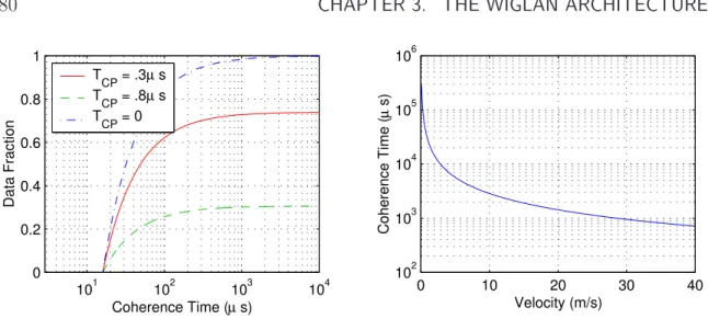
3.5 Effect of Coherence Time on Throughput . . . 76
3.6 Implications for the WiGLAN . . . 77
3.6.1 Number of Server Antennas . . . 77
3.6.2 Coherence Time . . . 79
3.7 Design Guidelines . . . 80
4 Circuit Optimizations 83 4.1 Sacrificing Capacity for SNR Gain. . . 84
4.1.1 Using SNR Gain to Ease Circuit Requirements. . . 84
4.1.2 SNR Gain vs. Antennas . . . 86
4.2 Link Budget Analysis . . . 87
4.3 Analog Circuit Optimizations . . . 89
4.3.1 Reducing RF Output Power . . . 90
4.3.2 Reducing RX Circuit Area . . . 91
4.3.3 Reducing RX Circuit Power Dissipation . . . 93
4.4 Digital Circuit Implications . . . 94
4.4.1 Reducing Digital Circuit Area . . . 95
4.4.2 Reducing Digital Circuit Power . . . 96
4.5 WiGLAN Analog Circuit Optimization . . . 97
4.5.1 SNR Margin from Link Budget . . . 97
4.5.2 Reducing Circuit Area . . . 98
4.5.3 Reducing Power Consumption . . . 101
4.6 Design Guidelines . . . 102
5 Circuit Crosstalk 105 5.1 Feedback Crosstalk Model . . . 106
5.1.1 Crosstalk Feedback Loop between Multiple Front Ends . . . . 106
5.1.2 Crosstalk behavior when ρ < 1. . . 109
5.1.3 Crosstalk behavior when ρ≥ 1 . . . 110
5.3.1 Crosstalk as a Static Fading Channel . . . 118
5.3.2 Role of the Singular Values . . . 119
5.3.3 Worst Case SNR Loss From Crosstalk . . . 121
5.3.4 Asymptotic Averaged SNR Loss From Crosstalk . . . 123
5.3.5 Effect of Crosstalk Phase Randomization . . . 127
5.4 Crosstalk Performance of Larger Systems . . . 130
5.5 How to Achieve Phase Randomization . . . 131
5.6 Circuit Crosstalk Measurements . . . 133
5.6.1 Frequency Nulls from Crosstalk Feedback. . . 133
5.6.2 Wideband RX Circuit Crosstalk Measurements . . . 135
5.6.3 Effect of Partial Phase Randomization . . . 136
5.7 Simulation Results . . . 137
5.8 Design Guidelines . . . 141
6 Peak to Average Power Ratio 143 6.1 Existing Solutions for Reducing PAPR . . . 144
6.2 PAPR Distribution and Clipping Probability . . . 146
6.3 Effect of PAPR on Amplifier Efficiency . . . 149
6.3.1 Some Example OFDM Symbols . . . 149
6.3.2 Instantaneous Amplifier Efficiency Curves . . . 150
6.3.3 Average Efficiency with Rayleigh Inputs . . . 151
6.3.4 Average Efficiency with Uniform Input . . . 154
6.3.5 Average Efficiency Curves . . . 155
6.4 Effects of Clipping an OFDM Symbol . . . 156
6.4.1 Discrete-Time Clipping Model . . . 157
6.4.2 SNR Degradation from Clipping . . . 159
6.4.3 Bandwidth Expansion from Clipping . . . 164
6.5 Precoding Algorithm for PAPR Reduction . . . 166
6.5.1 Precoding Connection to WiGLAN Downlink Protocol . . . . 166
6.5.2 The PAPR Precoding Algorithm . . . 168
6.6 Amplitude Synthesis for PAPR Reduction . . . 170
6.6.1 Capacity of Phase- and Magnitude-Only Channels . . . 171
6.6.2 The Phase Synthesis Algorithm . . . 174
6.7 Simulation Results . . . 178
6.7.1 Precoding Simulation Results . . . 178
6.7.2 Synthesis Simulation Results . . . 183
10 CONTENTS
6.8.1 Computational Complexity Comparisons . . . 185
6.8.2 Rate Loss Comparisons . . . 186
6.8.3 Amplifier Efficiency Comparisons . . . 186
6.8.4 Rate Normalized Efficiency Gain (High SNR) . . . 189
6.8.5 Rate Normalized Efficiency Gain (Low SNR) . . . 191
6.9 Design Guidelines . . . 192
7 Conclusions and Future Work 193 7.1 Thesis Contributions . . . 193
7.1.1 Network Architecture . . . 193
7.1.2 Circuit Area and Power Optimizations . . . 194
7.1.3 Circuit Crosstalk Mitigation . . . 194
7.1.4 Peak to Average Power Control . . . 195
7.2 Future Research Directions. . . 195
A Notation 197 B Tables of SNR Values 199 C Outphasing Amplifiers 203 C.1 Using Outphasing Amplifiers . . . 203
C.1.1 The Combining Circuit . . . 203
C.1.2 Vector Representation of a Signal . . . 205
List of Figures
1-1 The bottom layers of the communications stack, with a brick wall indi-cating the relative lack of interaction between the algorithm and analog hardware layers. We exploit some knowledge of analog hardware im-pairments to influence algorithm design. . . 22 1-2 Wireless system block diagram. The circuits and other hardware inside
the dashed rectangle are typically black boxed by the algorithm designer. 24
2-1 OFDM frequency bin shapes, with single bin highlighted. . . 29 2-2 Adaptive modulation per frequency bin vs. measured channel response. 31 2-3 The wireless channel model. . . 32 2-4 Path loss for n = 2, 3, 4 vs. distance. . . 34 2-5 Capacity comparison between 1× 1 and 4 × 4 wireless systems. . . . 35 2-6 Capacity tradeoff with SNR. . . 37 2-7 Outage probability for transmitting at rates of 6 b/s/Hz for 1× 1 and
4× 4 systems, and at 24 b/s/Hz (6 b/s/Hz per transmit antenna) for a 4× 4 system. . . 38 2-8 Diversity-multiplexing tradeoff for a 4× 4 system. . . . 39 2-9 Uncoded 64-QAM BER for 1× N systems, N = 1, 2, 4, 9, 16 (right
to left). . . 41 2-10 BER for a 1× 1 vs. 4 × 4 system for a 64-QAM input constellation. . 43 2-11 A typical analog transmit and receive front end. . . 44 2-12 Two methods for increasing the efficiency of a linear amplifier. Varying
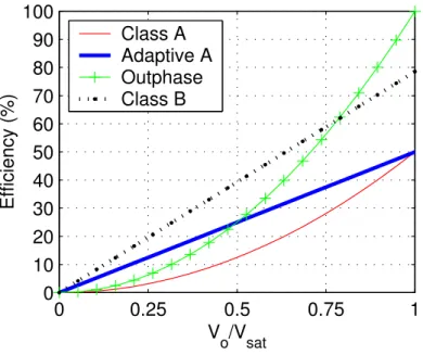
the bias currents changes the gain of the adaptive A amplifier (left), while an outphasing amplifier sums the outputs of two highly efficient, constant amplitude amplifiers (right). . . 46 2-13 Efficiency of several linear (Class A, Adaptive A, and Outphase)
am-plifiers vs. output voltage swing. The nonlinear class B amplifier is shown for comparison. . . 47 2-14 Rapp model for amplifier saturation (assuming unity gain). . . 48 2-15 Sinusoidal harmonics from the Rapp model. . . 49
12 LIST OF FIGURES
3-1 A schematic of a typical network, including both the high-bandwidth, multi-antenna nodes (B), as well as the less capable, power- and memory-limited nodes (A).. . . 53 3-2 The five phases of a communications frame. . . 54 3-3 Uplink BER performance for 4 (dashed line) and 16 (solid line with
dots) nodes for 64-QAM. The performance closely matches a 1× 1 system at high SNR. . . 56 3-4 Uplink uncoded 64-QAM BER performance for 4 nodes with extra
server antennas. From right to left, the curves represent 4, 5, 6, 7, and 8 server antennas. . . 59 3-5 Downlink precoding: all of the shaded constellation points are mapped
to the center constellation, so all the circled points are equivalent, for example. . . 61 3-6 Downlink BER performance for 4 (dotted line) and 16 (dashed line)
downlink nodes, with an equal number of server antennas. The diver-sity gain for an extra transmit antenna is also shown. . . 62 3-7 Bandwidth allocation for two nodes and several total power levels. . . 66 3-8 Concatenated code viewpoint for the uplink. One encoder outputs
the bit streams for each node antenna, with the inner and outer de-coders corresponding to the pseudoinverse and cancellation operations, respectively, of the VBLAST decoder. . . 68 3-9 Concatenated code viewpoint for the downlink. The outer and
in-ner encoders are the back-substitution and rotation operations, respec-tively, of the transmit precoder. . . 68 3-10 Achievable (left) and uncoded (middle, right, for 64-QAM) SNR gain
for 1× N and N × N systems for N = 2 to 5, relative to a 1 × 1 system. 70 3-11 BER curves (left plot) for a 1× 1 and 1 × 4 system for uncoded 4-, 16-,
64-, and 256-QAM constellation sizes (dashed, left to right), with BER curves for adaptive modulation at 10−3 BER (solid). Also plotted is
expected throughput vs. SNR for 10−5 (middle) and 10−3(right) BER,
respectively for 1× 1 to 1 × 5 systems (bottom to top). The horizontal dashed line represents 6.67 b/s/Hz, or 1 Gb/s for 150 MHz bandwidth. 71 3-12 Encoded BER for Reed-Solomon codes of varying lengths (left), and
optimizing code parameters for a given target BER using the (255,k) code family (right). . . 72 3-13 Circles represent the distance that the BER is not greater than some
threshold for direct (dashed) and server-assisted (solid) communication between nodes A and B for a fixed transmit power. . . 74 3-14 Multiplicative distance gain factor compared to a 1× 1 system for
and how the coherence time varies as the relative velocity changes (right). 80
4-1 BER for a 1× 1 vs. a 4 × 4 system for a 64-QAM input constellation. 85 4-2 Achievable ranges of 1× 1 to 4 × 4 systems. . . 86 4-3 Achievable and uncoded SNR gain for 2× 2 to 5 × 5 systems relative
to a 1× 1 system. Gains for single antenna nodes (middle) are also shown for comparison. . . 87 4-4 Roadmap for analog circuit optimizations. . . 90 4-5 Sizes of typical on-chip components (in parentheses) relative to the
bipolar transistor. . . 91 4-6 Simplified circuit comparison for narrowband (left) and broadband
(right) LNA (biasing not shown). The inductors in the narrowband LNA are replaced with physically smaller resistors and transistors. (Di-agram by L. Khuon) . . . 92 4-7 Example noise figure (solid) and LNA power gain (dashed) vs. bias
current. . . 94 4-8 Schematic for WiGLAN integrated receiver test chip with four RF
front ends. The LNA (highlighted) is the target for area and power optimizations. (Diagram by L. Khuon) . . . 98 4-9 Die photo of WiGLAN receiver chip with four RF front ends. The
boxed region is the area occupied by a single broadband LNA. (Chip design by L. Khuon) . . . 100
5-1 Crosstalk coupling model for two parallel amplifiers. . . 107 5-2 Three crosstalk cases for different values of the interferer/input ratio ρ.
Unfavorable crosstalk conditions can degrade the SNR for a large range of values, with ρ > 1 resulting in the crosstalk signal overwhelming the intended signal. . . 109 5-3 Some sources that can couple into an amplifier input. . . 112 5-4 Two- (left) and four-port (right) model for a circuit with scattering
matrix S. . . 113 5-5 Crosstalk model for a 1× 2 system. . . . 117 5-6 Effect of singular value ellipse on the input vector. . . 120 5-7 Singular values as a function of crosstalk magnitude (right) for 0 to
30 dB in 5 dB increments. Left side shows the range of singular val-ues for a small (solid) and large (dashed) crosstalk magnitude. The crosstalk phase is uniformly distributed. . . 121
14 LIST OF FIGURES
5-8 For a 2× 2 crosstalk matrix, lower bounds on performance degradation due to crosstalk (left plot) as a function of phase for 0 dB (solid), 10 dB (dash-dot) and 20 dB (dotted) isolation, and worst case performance as a function of crosstalk isolation (right). . . 122 5-9 PDFs of constellation points at ±d/2 in AWGN. The probability of
error P r(ǫ) is given by the integral of the shaded areas. . . 125 5-10 Asymptotic SNR loss for a 2× 2 crosstalk matrix averaged over all
inputs for a fixed crosstalk phase (left) for 0 (solid), 10 (dot-dash), and 20 dB (dotted) isolation. Right plot compares average (solid) to worst case performance (dashed) for θ = 180◦. . . . 128
5-11 Left shows performance of randomized phase algorithm (solid lines) for all inputs (thick) and worst case inputs (thin). Dotted lines show the unrandomized performance for comparison, and right plot shows equivalent crosstalk isolation. . . 129 5-12 Worst case (dashed) and randomized (solid) SNR loss for 3× 3 (left)
and 4× 4 (right) crosstalk matrices. . . . 131 5-13 Two possible hardware methods of adjusting the phase. . . 132 5-14 Die photo of PA test chip. (Chip design by A. Pham) . . . 134 5-15 PA test chip crosstalk measured for different phase shifts (left). The
thick solid line is inverse of amplifier gain for comparison. Depending on the phase, deep notches can appear at random places where the crosstalk is unfavorable (right). . . 135 5-16 Simulated data fits using measured crosstalk amplitude and phase
in-formation compared to the measured frequency response. . . 136 5-17 Measured crosstalk magnitude (left) and unwrapped phase (right) for
“close” (dashed) and “far” (solid) circuits. The crosstalk magnitude is correlated with but not a function of distance. . . 137 5-18 Average SNR loss for a 2× 2 system for a fixed phase (dashed, left)
and for randomization over the WiGLAN bandwidth (solid, left), or 50◦ centered on the fixed phase. Right plot shows the average SNR loss
for the worst case phase (0◦ or 180◦) with varying amounts of partial
phase randomization. Crosstalk isolation is 0, 5, 10, and 20 dB from bottom to top in both plots. . . 138 5-19 Worst (dashed), average (thick), and best (thin line) case crosstalk for
several isolations for a 1× 2 system. The dotted line represents no crosstalk. . . 139 5-20 Worst (dashed), average (thick), and best case crosstalk for several
isolations for a 1× 4 system. The dotted line represents no crosstalk. 140 5-21 Crosstalk at transmitter for a 2× 2 system using V-BLAST with 20 dB
6-2 Three examples of OFDM symbols with 128 frequency bins and 64-QAM constellations scaled relative to the RMS amplitude. Depicted are a “typical” OFDM symbol (middle), as well as unusually “good” (left) and “bad” (right) symbols. . . 150 6-3 Comparison of the efficiency of various amplifier topologies as functions
of the output magnitude (left) and power (right). . . 151 6-4 PDF of a Rayleigh distribution (left) with different average powers
(2σ2). Right shows the power savings relative to the average power
corresponding to no clipping.. . . 152 6-5 Average Efficiency for a Rayleigh distribution (left) and a uniform
distribution (right) vs. maximum PAPR. . . 156 6-6 Clipping of a digital signal x[n] is equivalent to adding a noise signal
e[n] given by the Fourier transform of the inverse signal. . . 157 6-7 Two peaks of the discrete-time, 128 bin OFDM symbol (left,solid) are
clipped to the threshold (left, dashed) level. The center plot compares the original frequency bin constellation points (◦) with the clipped symbol constellation points (×). Right plot shows the constellation point offsets caused by the clipping. . . 158 6-8 Constant offset caused by a single clip (left) shifts the resulting
con-stellation closer to a decision region boundary, increasing the error probability. A zoomed picture of a single constellation point and its decision region is shown on the right. . . 160 6-9 Average SNR loss due to clipping (left) and as a function of the
maxi-mum allowed PAPR (right) for length 128 OFDM symbols using (top to bottom) 4-, 16-, 64-, and 256-QAM constellations. Dashed lines indicate the worst-case behavior. . . 164 6-10 Cumulative maximum spectral heights for several clipping levels. The
6.2 dB and 10 dB levels correspond to the maximum PAPRs for a 10−2
clipping probability for the precoding algorithm (Section 6.5) and the original distribution. Right plot compares spectral heights to 802.11a transmitter spectral mask. . . 165 6-11 OFDM symbol with 10 frequency bins (left), and the corresponding
PAPR (right) for two different phase configurations. . . 167 6-12 Constellation mapping for transmit precoding with 16-QAM showing
16 LIST OF FIGURES
6-13 A typical constellation for the complex (left), magnitude-only (middle), and phase-only (right) channels. . . 173 6-14 POCS algorithm dynamics: the initial guess converges to a point in
the intersection of the two sets after repeated projections onto each set. The error signal e[i] decreases with each iteration. . . 176 6-15 Phase synthesis example comparing discrete-time signal (left) and
continuous-time signal (right). The thin line is the original signal, and thick line shows the result of the synthesis algorithm after 100 iterations. . . 178 6-16 Example of PAPR precoding using 10 iterations for the greedy and
random-greedy algorithm. Left plot shows the peak reduction with each iteration for the greedy (solid) and random-greedy (hollow) al-gorithm. Middle plot shows original signal, and right plot shows the result of the greedy algorithm. The middle circle represents the maxi-mum amplitude after using the random-greedy algorithm.. . . 179 6-17 Results for example PAPR precoding in Figure 6-16, showing how the
peak and average power changes result in PAPR improvements. Left two plots are for the greedy (1) and random-greedy (2) algorithm, and the right plot diagrams the original (1), greedy (2), and random-greedy (3) PAPR. . . 180 6-18 Histogram of PAPR reduction loss for random-greedy over greedy
al-gorithm for 20% (25) active bins and the average power gain needed for the greedy (right curve) and random-greedy (left curve) algorithm. 181 6-19 CCDFs for precoding algorithm using greedy and random-greedy
al-gorithms for length 128 OFDM symbols and 10× oversampling. The greedy algorithm uses 25 iterations maximum, and the random-greedy algorithms use 10%, 20%, and 50% bins active (right to left). . . 182 6-20 Iterations required for for 128 bins, 64-QAM, greedy (less than 1%
requires more than 10 iterations) and histogram of which bins are most likely to improve PAPR. . . 183 6-21 CCDF of the PAPR for the phase synthesis algorithm for length 128
OFDM symbols using 64-QAM and 10× oversampling for bandlimited interpolation. The difference between 10 (solid right) and 100 (solid left) iterations is less than 1 dB. . . 184 6-22 Precoding: Average Efficiency for Rayleigh distributed signals through
ideal linear amplifiers using length 128 OFDM time signals with 10× oversampling and 64-QAM. Histograms show original PAPR, plus PAPR of random-greedy and greedy algorithms (left to right) with 20% active bins or 25 maximum iterations. . . 187
C-1 Outphasing system (left) with Wilkinson combiner (right). . . 204 C-2 Vector combining of two constant amplitude signals in the outphased
amplifiers. . . 205 C-3 Triangle for sin/cos property. . . 207 C-4 Frequency spectrum of original signal (left) and outphase signal (right).209 C-5 Instantaneous power for bandlimited versions of the outphase signal. . 210
List of Tables
4.1 Sample link budget for a 1× 1 and 4 × 4 system for uncoded 64-QAM at 10−5 BER. . . 89 4.2 SNR margin in dB for adaptive modulation in the WiGLAN assuming
SNRi = 35.4 dB. Uncoded numbers are for rates in Mb/s for 10−5
BER. All indicated rates are normalized to show actual information rates. . . 97 4.3 Comparison of a single WiGLAN narrowband and broadband LNA. . 99 4.4 Area and noise comparison for 5 GHz single antenna receiver front ends
with both broadband and narrowband four antenna WiGLAN receiver front ends. (* approximate receiver area for a combined transceiver chip).. . . 99
6.1 Table of instantaneous and average efficiency for several types of am-plifiers. . . 155 6.2 Computational complexity for precoding and synthesis algorithms for
a sample OFDM symbol of length 128 using 64-QAM. (1 MFLOP is 106 FLOPS) . . . 185
6.3 Average efficiencies (%) for precoding and synthesis algorithms. . . . 188 6.4 Average energy units (original signal normalized to 100) required per
bit after using the precoding and synthesis algorithms in the high SNR regime. . . 190 6.5 Average energy units (original signal normalized to 100) required per
bit after using the synthesis algorithm in the low SNR regime. . . 191
B.1 Table for adaptive modulation SNR values (dB) for 1000, 900, and 540 Mb/s assuming a system bandwidth of 150 MHz with a uncorrected BER = 10−1. The throughput is normalized to account for the rate
20 LIST OF TABLES
B.2 Table for adaptive modulation SNR values (dB) for 1000, 900, and 540 Mb/s assuming a system bandwidth of 150 MHz with a uncorrected BER = 10−2. The throughput is normalized to account for the rate
loss of the (255,k) RS codes. . . 200 B.3 Table for adaptive modulation SNR values (dB) for 1000, 900, and 540
Mb/s assuming a system bandwidth of 150 MHz with a uncorrected BER = 10−3. The throughput is normalized to account for the rate
loss of the (255,k) RS codes. . . 201 B.4 Table for adaptive modulation SNR values (dB) for 1000, 900, and 540
Mb/s assuming a system bandwidth of 150 MHz with a uncorrected BER = 10−4. The throughput is normalized to account for the rate loss of the (255,k) RS codes. . . 201 B.5 Table for adaptive modulation SNR values (dB) for 1000, 900, and 540
Mb/s assuming a system bandwidth of 150 MHz with a uncorrected BER = 10−5. The throughput is normalized to account for the rate
loss of the (255,k) RS codes. . . 202 B.6 SNR gain (dB) for N × N systems compared to a 1 × 1 at the same
capacity. . . 202 B.7 SNR gain (dB) for uncoded systems compared to a 1× 1 at the same
Chapter 1
Introduction
In all but the simplest systems, it is often necessary to separate the design into many layers separated by abstraction barriers. The abstraction barriers isolate the details of a section of the system from all other system parts. These layers form a stacked protocol, in which a layer can only communicate with the layer immediately above and below it. In principle, all of the implementation details within a given layer are hidden from any layer above or below it. This allows a designer to focus on designing the algorithms in his/her own layer without having to know how the entire system is going to work. In addition, the layering allows the algorithms in a particular layer to be changed without affecting any of the other layers, enabling algorithm reuse for many different applications, as well as allowing improvements to be made without disrupting existing infrastructure.
In practice, however, this strict layering can cause design choices in one layer to make unreasonable demands on the neighboring layers. For this reason, the design in each layer often incorporates some knowledge of the details of nearby layers. The amount of information that is shared between the layers depends on their proximity, with neighboring layers more likely than distant layers to share information.
1.1
The Hardware Abstraction Layer
For a communications system, Figure 1-1 represents the bottom few layers of the protocol stack (adapted from the TCP/IP stack). The Physical layer is the bottom-most layer, and is concerned with how the data passed to it from the MAC (Media Access Control) layer is going to be transmitted and received. At the transmitter, the Physical layer receives a bit stream and processes it to an analog waveform to be transmitted. At the receiver, the Physical layer receives an analog waveform from the communications channel, and converts it back into a bit stream, which is passed to the layer above. In this thesis we will focus on aspects of the Physical layer.
22 CHAPTER 1. INTRODUCTION
This Thesis
Physical Analog Hardware Algorithms Digital Hardware Network
MAC/Link
Figure 1-1: The bottom layers of the communications stack, with a brick wall indicating the relative lack of interaction between the algorithm and analog hardware layers. We exploit some knowledge of analog hardware impairments to influence algorithm design.
The Physical layer can be further subdivided into algorithm, digital, and analog hardware implementation layers. Although these layers do not officially exist, they are present in practice as algorithms, digital and analog hardware are all typically designed with only limited information about the other layers. The algorithm designer usually works in the theoretical realm, where precision can be exact and linearity is perfect, with infinite dynamic range and noise is absent or artificially introduced. These algorithms are then implemented on digital hardware, and then output through the analog hardware to interface with a communications channel. Each of these steps is separated by an abstraction barrier, but the strength of these barriers is very different.
Digital circuit designers must contend with issues of power, computational com-plexity and speed, dynamic range, and quantization errors. If the algorithm designer is aware of these limitations, the algorithms can be designed to be less computation-ally taxing or more tolerant to quantization errors. Similarly, the digital hardware designer can optimize the circuit architecture for running a particular type of algo-rithm so that it is more efficient for the given task. Because of these advantages, the algorithms and digital hardware are often designed with each other in mind.
Analog circuit designers must also contend with hardware that is far from ideal. For example, issues of nonlinearity, limited dynamic range, component noise and crosstalk, and power efficiency can all hinder analog circuit performance. The algo-rithm designer, unaware of the nature of this nonideal behavior, may place unrealistic demands on the analog hardware while optimizing algorithm performance, requiring large design margins for the hardware to function. Unlike with digital circuits, ana-log circuitry cannot be automatically synthesized, with difficult requirements placing greater demands on the circuit designer. In addition, analog circuits are tuned to
representing the weak abstraction barrier which allows significant details about each layer to be shared. On the other hand, a brick wall separates the analog hardware layer from the digital hardware and algorithm designer, representing the very strong abstraction barrier that separates them. The algorithm designer is already one layer removed from the analog hardware, and due to the large differences in technical knowledge required, fewer of the details of the analog hardware design passes up to the algorithm designer. For example, the algorithm designer will often have a model of the nonideal circuit behavior, but without detailed enough knowledge to know how changing the circuit specifications will affect other circuit parameters. This thesis attempts to bridge this gap by using some knowledge of analog hardware impairments and implementation to guide algorithm design.
Removing the abstraction barrier would seem to be a good solution, since a joint optimization should be better than optimizing each layer individually. Removing the layering allows more optimization, but at the cost of a greatly increased workload on the system designer. However, even some cross-layer knowledge can significantly increase the efficient use of resources. Many things are easier to do digitally than with analog components, but the digital versions may come at the expense of circuit size and power. Similarly, there are many tasks that are well-suited to analog circuit techniques and cannot easily be done with digital circuits.
As a general rule, the different specifications of a design are not all equally difficult to meet, thus the performance of a system is limited by its most difficult to meet constraint. By understanding some details of the circuit behavior, the algorithm designer can learn which specifications are particularly difficult for the analog circuit designer to meet, and which are easy to meet. The excess margin from the easier to meet constraints can then be traded off to relax the more difficult design constraints, leading to novel architectures and improved designs. Significant gains in power and area can be made with these cross-layer designs. The effects of nonidealities from the analog circuits can be reduced by these techniques as well. We explore several problems that can occur with analog circuits and algorithmic techniques that can either alleviate or are tolerant of these limitations.
1.2
High-level Physical Layer System View
A block diagram of a typical wireless system is shown in Figure1-2. The data stream to be transmitted is first encoded to provide error protection, modulation, pulse shap-ing, etc. in the digital domain. The digital waveform is then converted to analog and
24 CHAPTER 1. INTRODUCTION passband & amplify digital to analog mix to analog to digital
Encode mix to Decode
baseband amplify &
Analog Front End Analog Front End
x H y
Figure 1-2: Wireless system block diagram. The circuits and other hardware inside the dashed rectangle are typically black boxed by the algorithm designer.
mixed up to the carrier frequency. A power amplifier (PA) drives the signal onto the antennas and through the wireless channel. At the receiver, the signals picked up by the receive antennas are then amplified by a low noise amplifier (LNA) and mixed back down to a baseband signal. This waveform is then sampled by the ana-log to digital converter. The shaded boxes are part of the anaana-log front ends, which are squarely in the domain of the analog circuit designer. For the communication algorithm designer, the entire dashed box is usually abstracted away into a simplified wireless channel model. Hardware impediments are encapsulated by simplified mod-els, which do not capture the interdependence of the different circuit characteristics. As we will show, some cross-layer knowledge allows the system to be improved in circuit area and power, and more resistant to circuit nonidealities.
1.3
The WiGLAN
For wired networks, gigabit per second (Gb/s) Ethernet networks are already com-mercially available. Although the wireless channel is much more hostile than the wired one, it would be desirable to have such a high bandwidth connection for wireless net-works as well. Such a network might be the Wireless Gigabit LAN (WiGLAN) [14].
A central server with few constraints on transmit power, computational ability or memory controls and assists the peer-to-peer traffic among the multiple mobile nodes in the network. The nodes have limited battery and computational power, and are equipped with one or more antennas for transmission and reception. The central server is equipped with several antennas (for example, four), which can be used in any combination to transmit and receive information from the other nodes in the system. Within the WiGLAN, appliances throughout the home or office environment can communicate wirelessly among themselves and to the central network controller. Depending on the needs and type of each node, single and multiple antenna battery-powered portable adapters are attached to the various appliances. Devices that re-quire high data rates and/or excellent link quality for large ranges (e.g. an HDTV or
150 MHz. The wide bandwidth means that the network only needs to be able to achieve an overall spectral efficiency of about 6-7 b/s/Hz. However, the wide band-width also brings frequency selective fading and complexity issues which must be dealt with. For these reasons, and to facilitate resource allocation, the total bandwidth is divided into many subcarriers, or frequency bins through Orthogonal Frequency Di-vision Multiplexing (OFDM).
1.4
Thesis Outline and Contributions
In the following chapters, we explore in detail the implications and advantages of opti-mizing algorithms across the analog circuit abstraction barrier within the framework of the WiGLAN.
The wireless channel model is described in Chapter2, both for single- and multiple-antenna links. The achievable performance is shown, as well as the trade offs involved in power, data rate, and error tolerance. Some basic circuit principles are also de-scribed to provide the necessary cross-layer knowledge of the analog circuitry.
Chapter 3 introduces the system architecture of the WiGLAN and the communi-cations protocol it uses. Because of the asymmetrical capabilities of the nodes and the central server, the majority of the computation and memory requirements have been offloaded to the server. The uplink/downlink protocol allows the network nodes to achieve multiplexing gain without coordination, reduce transmit power, and increase transmission range by exploiting the capabilities of the central server.
Chapter 4 describes some of the limiting constraints for circuit area and power of receiver circuit designs. The SNR gain from using multiple antennas can be used to reduce the analog circuit area or power. Removing physically large passive com-ponents can reduce circuit area by a factor of three, while reducing bias currents to lower amplifier gain cuts amplifier power consumption by a factor of two or more. Gains in area and power can also be made for digital circuits by using the SNR gain to reduce the computational complexity.
Chapter 5 describes the effect of crosstalk between parallel circuits, with design guidelines as well as techniques to mitigate the severity of circuit crosstalk. This is especially important when there are parallel amplifiers present in a circuit which may create unstable feedback loops. A simple relationship between amplifier gain and crosstalk isolation prevents deep nulls or unstable feedback behavior for parallel circuit paths. A relation for the asymptotic SNR loss caused by the crosstalk is derived, and the beneficial effects of phase randomization is explored.
26 CHAPTER 1. INTRODUCTION
Chapter 6outlines the problem of the high dynamic range requirements of many wideband systems including the WiGLAN, with the associated problem of poor am-plifier efficiency for these waveforms. Peak to average power reducing algorithms, both with and without penalties in data rate are described which reduce the dynamic range requirement and significantly increases overall power efficiency. A precoding algorithm decreases the energy per bit requirement by more than a factor of three when coupled with an efficient linear amplifier at high SNR. At low SNR a synthesis algorithm achieves similar gains. It is also shown that the major distortion caused by hard signal clipping is not a loss in SNR, but instead bandwidth expansion.
Chapter 2
Background
Since the WiGLAN system has 150 MHz of bandwidth, the spectral efficiency re-quired to achieve data rates at or near a gigabit per second is less than seven bits per second per Hertz of bandwidth (b/s/Hz). Although it may be possible to transmit at or above this rate over some of the frequency band, the frequency- and time-dependent nature of the wireless channel requires adaptively changing the encoding to match the channel conditions. Dividing the available bandwidth into frequency bins via OFDM is described, as well as the achievable limits of the communication links. In addition, a brief overview is given for some of the nonidealities that must be accounted for in analog circuitry, along with some of the major concerns for both analog and digital circuit designs. This knowledge presents opportunities for algo-rithms to take advantage of circuit details that are often otherwise hidden from the algorithm designer.
2.1
Transmission via OFDM
Although the WiGLAN has a large amount of bandwidth to work with, it is not feasible, or even desirable for each transmitter to use all of the available bandwidth for each transmission. In a multi-user environment, it is inefficient for each user to be assigned time slots in which the entire frequency bandwidth is available for use. In addition to the requirement of much faster data converters and hardware to process data so quickly, the multipath fading over such a large bandwidth is not independent of frequency. It then becomes necessary to train and equalize the signals for the path between any two nodes which might be transmitting. This is especially taxing for small mobile nodes with very limited computational power and low data requirements. Additionally, even if the node has the capability to process the entire band, it might not need all of the available bandwidth, wasting the surplus for that time slot.
Modu-28 CHAPTER 2. BACKGROUND
lation (QAM) on the subcarriers of an OFDM symbol. The advantage of OFDM is that the symbol is divided into a large number of frequency bins or subcarriers which can then be allocated to the nodes that wish to communicate at a given time in ratios according to their requested rates. The bandwidth of each frequency bin is small enough that the the multipath fading is essentially constant over the bin, reducing the equalization to only a single multiplicative constant to account for the amplitude and phase shift of that subcarrier.
2.1.1
Shape of OFDM Frequency Bins
A convenient subchannelization for an OFDM symbol is to use the frequency bins of a Discrete Fourier Transform (DFT). To convert the modulated subcarriers (frequency bins) into a time signal, one can simply apply the Inverse Fast Fourier Transform (IFFT), which has complexity that grows with O (N log N) where N is the number of frequency bins. At the receiver, the Fast Fourier Transform (FFT) will convert the OFDM time symbol back to frequency bins, again withO (N log N) complexity.
As shown in Figure 2-1, these frequency bins have the shape of a sin(x)/x pulse, which are orthogonal to each other, but have side lobes that fall off very slowly as 1/x. As a result, if there is any kind of inter-symbol interference (ISI), then a frequency bin will interfere significantly with neighboring bins. To deal with the impulse response of the channel, a cyclic prefix can be prepended to the OFDM symbol, which has the effect of making the convolution of the OFDM symbol with the channel impulse response the same as the circular convolution. When the OFDM symbol is transformed to the frequency domain, each sample (frequency bin) is simply scaled by a complex number that is the channel frequency response at that frequency. As long as the prefix length is at least as long as the channel impulse response, this property holds, even if the channel characteristics change with every symbol. In order to be able to correct for the channel, however, there still needs to be some training data sent along with each OFDM symbol.
This is a very optimistic result, however, and not always true in practice because the length of the channel impulse response will invariably be longer than the chosen prefix length, or the required prefix length will be so long that it significantly impacts the data rate. The cyclic prefix then serves to reduce the ISI, making equalization easier, but not eliminating it altogether.
2.1.2
The Cyclic Prefix
If the channel impulse response is not finite length (or is very long), then the cyclic prefix will be so large that the code rate of an OFDM symbol becomes too small. If the frequency bins were more localized in frequency, then less work could be put
Figure 2-1: OFDM frequency bin shapes, with single bin highlighted.
into removing the ISI caused by the channel. In the extreme, the frequency bins could not overlap at all, but that makes the time series associated with each channel arbitrarily long. Although arbitrary subchannel shapes can be used as long as they are orthogonal, it is desirable to have an efficient algorithm, such as the FFT, to easily code and decode the OFDM symbol. The length of the cyclic prefix is dependent on the delay spread of the wireless channel, which is a measure of the average impulse response of the channel.
OFDM works well in the wireless domain because the delay spread in the channel is not considerable compared to the symbol duration as long as the signal bandwidth is relatively narrow. In a relatively wide bandwidth system like the WiGLAN, the cyclic prefix needed to combat ISI can be a significant fraction of the total symbol time [30].
2.1.3
Size of the OFDM Frequency Bins
The measure of how small a frequency bin needs to be to have essentially flat (fre-quency nonselective) fading is the coherence bandwidth, which in the 5 GHz band has been measured to be about 10 MHz for line of sight transmissions and about 4 MHz for transmissions without line of sight [39]. This suggests that the frequency bins should not be more than 4 MHz wide. There is a trade off in the number of frequency bins, since narrower bins facilitate resource allocation and are more likely
30 CHAPTER 2. BACKGROUND
to experience flat fading, but the larger number of bins requires more computations. Because the number of frequency bins is the length of the IFFT input, increasing the number of frequency bins also increases the resulting symbol duration. More fre-quency bins will also increase the peak to average power of the resulting time signals, which places increased demands on the capabilities of the analog front ends.
The computational penalty for a larger number of frequency bins is offset by potential for increased parallelism. Since each bin can be decoded individually, a large number of slower, cheaper processors can be employed rather than a single expensive one. More frequency bins also allows finer granularity in the data rates that can be assigned to individual nodes, and make it easier to reject a narrowband interferer by only masking out a small chunk of frequency.
With the flat fading of the frequency bins, all that needs to be measured is the frequency response of the channel, which can be learned from training data included at the start of each packet. The receiver does not need a separate equalizer to equalize the channel, since each frequency bin can be equalized by multiplying with the appro-priate constant. Even if the channel characteristics are different with every packet, since training data is always present, the channel parameters can be estimated. If an equalizer was used, then it might not be able to keep up with the changing channel parameters. This greatly reduces the amount of computation needed by a node to transmit, and the amount of training and computation needed increases with the requested data rate, so low-rate devices do not need to do as much calculation as a high-rate device, and can therefore be smaller and simpler. With all of the frequency bins, it is also possible for a node to slowly hop in frequency by being assigned different frequency bins over time by the central server.
2.1.4
Adaptive Modulation
The frequency bins also allow the system to adaptively deal with time variations in the channel. If a bin has a large amount of interference from outside sources (such as from a nearby, but separate, network), then the central server can neglect to allocate that bin to any node wishing to transmit. Additionally, if the data rate requested for a node varies with time, then additional frequency bins can be added or subtracted from the bandwidth allocated to that node to account for the change in the data rate. The node could instead be allocated differing numbers of time slots to vary its data rates as well. The modulation for each subcarrier can also adaptively change given the current signal to noise ratio (SNR) (such as 256-QAM for a bin with a very high SNR, 4-QAM for a bin with low SNR, or no transmission at all for a very noisy frequency bin) to maximize the amount of data that can be transmitted at a given time.
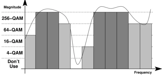
16−QAM 64−QAM 4−QAM Don’t Use Frequency
Figure 2-2: Adaptive modulation per frequency bin vs. measured channel response.
a hypothetical channel frequency response. The curved line is the frequency response of the channel, and the rectangular boxes represent idealized frequency bins. The shaded bins have been allocated according to the magnitude of the frequency response. If there is a deep fade (such as in the fifth bin), then that bin is not used at all.
This adaptive modulation approaches the optimal waterpouring scheme from a capacity standpoint [11]. However, most of the capacity can be achieved by simply deciding whether or not to use a use a frequency bin based on its relative SNR, and then using the largest supportable modulation across all of these bins. In Figure 2-2, the dark shaded bins show one way to do this. The total raw data rate for this particular channel is 64 b/s. If we use only the dark shaded bins, the data rate will be 40 b/s. If, on the other hand, we use all bins that can support 64-QAM, the data rate can be 48 b/s. This is a fairly simple optimization problem, but it saves the transmitter and receiver having to agree on the modulation for each individual bin. It is important to note that this threshold is in general different for each node as well as for each packet transmitted.
2.2
The Wireless Channel Model
The wireless channel is modeled as an equivalent discrete-time baseband system, as shown in Figure 2-3. An M × N system has M transmit and N receive antennas, resulting in M N distinct wireless channels. The system can be modeled as y = Hx+n. Here, x = [x1x2x3 · · · xM]T, where xi is the symbol transmitted from the ith antenna.
32 CHAPTER 2. BACKGROUND RX αΜ1 1 1 Μ Ν x y TX α11 αΜΝ
x
y
H
n
Figure 2-3: The wireless channel model.
antennas, and the channel is a matrix H, where hij = αij is the fading constant
between the ith transmit and jth receive antenna.
Each receive channel is given by yj = Piαijxi + nj, where xi is the (usually
complex) transmitted signal, αij is the channel fading parameter, and nj is noise.
The noise is modeled as complex Gaussian white noise with zero mean and variance N◦/2 in each dimension. This corresponds to the thermal noise of the amplifiers at
each receive antenna. The channel fading parameter is also a complex zero mean Gaussian variable with variance 1/2 in each dimension. Equivalently, the amplitude of αij is Rayleigh-distributed with unit mean and uniformly distributed phase. This
models a system in which there is no line of sight path between the transmitter and receiver, so all the energy from the transmitter arrives with random phases from all directions.
The value of nj is randomly chosen according to its probability distribution at
every channel use, but αij is constant over an entire packet of data (block fading).
The fading constant is independent and identically distributed between packets. Thus for each packet, the system only needs to learn the statistics of the channel once, but it must relearn them for every packet. The value of αij is randomly chosen for each
packet and each channel, so for multiple antenna systems, all channels are independent and identically distributed. We use N (m, σ2) to denote a Gaussian random variable
with mean m and variance σ2, and similarly Nc(m, σ2) to denote a corresponding
complex Gaussian random variable with mean m and complex variance σ2.
Not included in the channel matrix H is the path loss associated with the physical separation plus any power absorbing material between the transmitter and receiver. The average signal power at the receiver front end input is
The path loss is a function of the carrier wavelength λ, transmitter-receiver dis-tance d, and loss exponent n and is given by [55]
PL= 20 log10 µ 4π λ ¶ + 10n log10µ d d◦ ¶ . (2.2)
While the path loss exponent n depends on the particular propagation environment in effect, n = 3 is used as a typical choice for an indoor office environment. Typically, the loss at d◦ = 1 m is measured and losses at a distance greater than 1 m are related
through the second term of (2.2). Figure 2-4 plots the path loss as a function of the transmitter-receiver separation for various values of n assuming a carrier frequency of 5.25 GHz. The path loss for isotropic free space radiation is n = 2, while n = 3 corresponds to a Rayleigh fading environment with no line of sight signal. Higher values for n represent more severe path losses caused by obstructions such as walls and floors, although it is possible for the path loss to decrease even slower than in free space [38]. At a distance of 10 m, there is a a 10 dB difference in the path loss for each integer increment of n, so the choice of n can make a significant difference in the modeled performance of system. Measured indoor channel parameters for a house [40] and office [41] environment show values of n up to n = 7, with n = 3 being representative of most conditions. Some indoor channel measurements suggest that the constant term of (2.2) is an overly pessimistic model of actual conditions [40], but that the n = 3 exponent is still valid.
2.3
Capacity of a Wireless Link
After dividing the available bandwidth via OFDM, each frequency bin now has es-sentially frequency-independent fading. We can thus look at the capacity of a single bin by treating the fading as independent of frequency in each bin.
The capacity of a wireless link increases roughly linearly with the number of trans-mit and receive antennas [17]. However, this increase in capacity will only materialize with sufficient coding of the input data, which can greatly increase encoding and de-coding complexity. For a single channel usage, the maximum achievable data rate is given by C = M X i=1 log2(1 + λiSNR) , (2.3)
34 CHAPTER 2. BACKGROUND 1 5 10 15 20 40 50 60 70 80 90 100 Distance (m) Path Loss (dB) n = 3 n = 2 n = 4
Figure 2-4: Path loss for n = 2, 3, 4 vs. distance.
where the λi’s are the (possibly zero) eigenvalues of H†H(with H†being the conjugate
transpose of H), and SNR is the received signal to noise ratio [66]. Alternately, the λi’s are the squares of the singular values of H. Since the channel is going to be used
many times, we are interested in the maximum achievable throughput that we can expect for a given SNR. This is the ergodic capacity, and is only achievable with long codewords that span many different fades, or realizations of H. This is counter to the block fading model that we are using, but serves as a useful metric to compare against. Alternately, for data blocks that only experience a single fade (as in the block fading model) we can look at the outage probability, or how likely the channel is not going to be able to support a given rate.
2.3.1
Ergodic Capacity
The ergodic capacity for an M× N system in b/s/Hz can be written as [66] C = E " M X i=1 log2(1 + λiSNR) # , (2.4)
where the expectation is over all H. Figure2-5 shows the significant difference in the capacity curves for a 1× 1 and a 4 × 4 system. When the SNR is sufficiently high,
0 10 20 30 40 50 60 70 0 10 20 30 40 50 60 SNR (dB) Capcity (b/s/Hz)
Figure 2-5: Capacity comparison between 1× 1 and 4 × 4 wireless systems.
(2.4) can be simplified to C ≈ E " k X i=1 log2(λiSNR) # , (2.5)
where k is the number of nonzero eigenvalues. With high probability, H is full rank, so k = min(M, N ) [17]. Since the SNR is a deterministic value
C ≈ k X i=1 E [log2(λi)] + k X i=1 E [log2(SNR)] = k X i=1 E [log2(λi)] + k log2(SNR) . (2.6) If we define k log2(β) = k X i=1 E [log2(λi)] , (2.7)
then (2.6) can be simplified to
36 CHAPTER 2. BACKGROUND
The variable β is a constant that determines the offset of the capacity curve, and is dependent on the specific characteristics of the channel matrix H. The parameter β can also be written as the kth root of the expected determinant of H†H. If H is
a square matrix with Rayleigh-distributed entries, then the value of this expected determinant is k! [15].
In the high SNR regime, the change in capacity ∆C is given by
∆C = C − C′ ≈ k log2 µ βSNR βSNR′ ¶ = k[log2(SNR)− log2(SNR′)] = k 10 log10(2) (10 log10(SNR)− 10 log10(SNR′)) = k 10 log10(2)(SNRdB− SNR ′ dB) = k 10 log10(2)∆SNRdB, (2.9)
where ∆SNRdB is the difference in SNR in dB. Simplifying results in
∆C ≈ .33k∆SNRdB. (2.10)
This is the amount of capacity that must be sacrificed when reducing the signal to noise ratio from SNR to SNR′. As a result, every 3 dB reduction in SNR costs k b/s/Hz in capacity.
For example, referring to Figure 2-6, a 1× 1 system at an SNR of 20 dB has a capacity of 6 b/s/Hz. For a 4× 4 system at the same SNR, the capacity is 22 b/s/Hz. Using (2.10), this capacity difference of 16 b/s/Hz results in an SNR gain of 48.5 dB from the 1× 1 system. Comparing this to the 1 × 1 curve in Figure 2-6, a capacity of 22 b/s/Hz requires approximately 69 dB SNR for a 1× 1 system, a difference of 49 dB. However, physically achieving this SNR with an actual system would require a tremendous amount of transmit power for any reasonable transmitter-receiver sep-aration. Thus the 4× 4 system is able to reduce the required transmit power by more than a factor of sixty thousand compared to a 1× 1 system for the same data rate.
The expression for capacity in (2.4) requires an expectation over all realizations of H. In order to achieve the data throughput allowable according to the channel capacity, information bits need to be coded in blocks that are allowed to grow to very long lengths so that each block experiences many different fades. If a block only experiences a single fade, the instantaneous capacity may be below the ergodic capacity shown in Figure2-5.
0 10 20 30 40 50 60 70 0 10 20 30 40 50 60 SNR (dB) Capcity (b/s/Hz) C ∆SNR
Figure 2-6: Capacity tradeoff with SNR.
2.3.2
Outage Probability
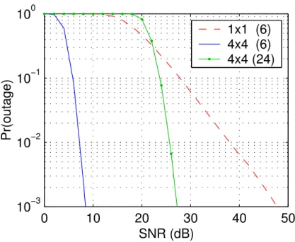
In a wireless network, there is a limit to how much delay can be tolerated, so the code blocks cannot reach arbitrarily long lengths, limiting how powerful the codes can be in terms of error correction capability. Since the transmitter might not know beforehand the channel conditions, a particular block may be transmitted during a fade that is deep enough that the channel is not able to support the data rate. This is an outage event, and the outage “capacity” in this sense is the highest rate that is achievable with a given probability for a given SNR. Figure2-7 plots the probability of outage versus SNR for a 1× 1 and a 4 × 4 system. The outage probability curves asymptotically become straight lines with a slope of−MN [71]. As with the ergodic capacity plots, the 4× 4 system shows a significant improvement in performance over the 1× 1 system. At an outage probability of 1%, the 4 × 4 system is over 40 dB better than the 1× 1 system for a total transmission rate of 6 b/s/Hz. Additionally, the curve for the 4× 4 system transmitting at 24 b/s/Hz (6 b/s/Hz per transmit antenna) also shows an improvement of over 10 dB compared to the 1× 1 system.
2.3.3
The Diversity-Multiplexing Tradeoff
The ergodic capacity is the maximum achievable data rate a system is able to support for a given SNR with arbitrarily low error rates. It assumes that the code words
38 CHAPTER 2. BACKGROUND 0 10 20 30 40 50 10−3 10−2 10−1 100 SNR (dB) Pr(outage) 1x1 (6) 4x4 (6) 4x4 (24)
Figure 2-7: Outage probability for transmitting at rates of 6 b/s/Hz for 1× 1 and 4 × 4 systems, and at 24 b/s/Hz (6 b/s/Hz per transmit antenna) for a 4× 4 system.
are able to grow infinitely long to experience many fades, resulting in the channel’s average behavior. On the other hand, the outage probability shows how quickly the error probability decays with SNR for a fixed data rate. There is a trade-off between these two fundamentally different ways to approach the limits of the wireless channel. This tradeoff between the multiplexing and diversity is described in [82].
The multiplexing gain describes how the capacity increases with SNR, and is defined as
r = lim
SNR→∞
R(SNR)
log(SNR), (2.11)
where R(SNR) is the achievable data rate as a function of SNR. Comparing this to (2.8), we see that r = min(M, N ). It should also be noted that a fixed data rate scheme (such as 64-QAM) results in r = 0. Intuitively, as the SNR increases in the case where r = 0, all the extra capacity gained is used to provide maximum redundancy for robustness to errors, so the diversity gain will be as large as possible. The diversity gain describes the slope of the error probability curve (on a log scale), and is defined as
d =− lim
SNR→∞
log(Pe(SNR))
0
1
2
3
4
0
2
4
6
8
10
12
Multiplexing Gain (r)
Diversity Advantage (d)
(4,0)
(3,1)
(2,4)
(1,9)
Figure 2-8: Diversity-multiplexing tradeoff for a 4× 4 system.
where Pe(SNR) is the probability of error as a function of SNR. Since d is the slope
of the error probability, we see that the probability of error asymptotically can fall as fast as SNR−d. The case of d = 0 means that as the SNR increases, the probability of error does not grow smaller. Intuitively, when d = 0, all of the extra capacity from the increasing SNR is used to transmit at higher rates, so there is no rate left to use for redundancy to increase robustness to errors.
These two endpoints, when r = 0 and d = 0 comprise the extreme values of the achievable (r, d) pairs. There are a whole range of achievable pairs in between these two extremes, however. Figure 2-8 plots the diversity-multiplexing tradeoff for a 4× 4 system, showing that the maximum diversity gain is 16 and the maximum multiplexing gain is 4. In general, (r, d) pairs of the form (r, (M − r)(N − r)) can be achieved [82]. The points on the lines connecting these discrete points can be achieved by timesharing between the endpoints.
For the purposes of this thesis, however, we will be focusing on the maximum diversity and maximum multiplexing endpoints. It should be noted that two schemes that achieve the same diversity gain d may still have a constant SNR offset due to the coding gain. Similarly, a coding scheme that achieves the maximum multiplex-ing gain r = min(M, N ) may not necessarily achieve the ergodic capacity given by (2.4). Nevertheless, a simple scheme that achieves the maximum available diversity or multiplexing is desirable for its efficient use of resources.
40 CHAPTER 2. BACKGROUND
2.3.4
Uncoded Bit Error Rate Performance
Any data rate smaller than the capacity given by (2.4) can be transmitted with arbitrarily low probability of error but requires large block size and computationally intensive encoding and decoding. If computation or memory resources are scarce, then encoding and decoding the data streams becomes difficult. An additional and more fundamental problem is that of delay. In order to encode with very long block lengths, the transmitter must first accumulate enough data. Similarly, the receiver must accumulate a full block’s worth of symbols before any bits can be decoded. For a low-bandwidth node, a large block size can require unacceptable amounts of delay. For example, a cordless phone or an intercom requires low latency for two-way communications. Since these are low-bandwidth devices, they should only be assigned one frequency bin. With a 1 MHz channel, there can be several megabits of available data rate. However, since the information rate is only a few kilobits per second, it can take a significant fraction of a second to accumulate enough bits to fill up an information block for transmission and again for reception.
At the other end of the spectrum, uncoded transmissions have the minimum delay, since information can be transmitted as soon as data is ready and decoded immedi-ately upon reception. The cost of uncoded transmissions is lack of any redundancy of error protection, though at high enough SNR this redundancy is unnecessary. Since the capacity of multiple antenna systems can be so high, it is reasonable to trade off some of the excess to reduce the amount of coding required. As lower bounds to performance, we can also examine the performance of uncoded (or minimally coded) data streams and compare to that of optimally coded systems.
In an uncoded system, the focus is not on capacity but diversity, or how quickly the receiver BER falls with respect to SNR. In general, the number of independent wireless channels that a bit experiences is the order of diversity it can see. Because the bit experiences multiple channels, it effectively sees an averaged channel, which has a lower variance than the individual channels. An alternate viewpoint is that it is less likely for all of the channels to be bad (deeply faded) than for a single channel. Although there are many ways to achieve high diversity, only spatial diversity will be considered in this thesis. Time diversity increases delay by requiring interleaving of data across many packets due to the block fading model, while frequency diversity uses up valuable bandwidth by coding across subcarriers. Spatial diversity does require additional hardware, but Chapter 4will show how this cost can be reduced.
For a single transmit antenna and a single receive antenna (a 1× 1 system), the uncoded bit error performance Pe ∝ 1/SNR, where SNR is the ratio of total
trans-mitted power P to the noise variance N◦ [71]. By increasing the number of receive
antennas, not only is there a gain in SNR from the increased received power, but more importantly, the slope of the bit error rate (BER) curve increases due to the
0 10 20 30 40 50 60 70 10−6 10−5 10−4 10−3 10−2 E s/No (dB)
Bit Error Rate
1x4 1x9 1x16
Figure 2-9: Uncoded 64-QAM BER for 1× N systems, N = 1, 2, 4, 9, 16 (right to left).
increased diversity. Figure 2-9 plots the BER curves (adapted from a closed-form formula in [51]) for uncoded 64-QAM constellation points transmitted with average power Es and received by N antennas. For each of these curves, the diversity gain
is d = N . Increasing the number of transmit antennas similarly increases the slope of the BER curve, but the transmit power per antenna is lowered to keep the total transmit power constant for a fair comparison.
For an M × N system in a Rayleigh-fading environment, the maximum diversity achievable is M N , which means the BER is proportional to SNR−M N [71]. Maximum diversity reduces the achievable data rate to that of a 1× 1 system, but it requires very little added complexity at the transmitter and receiver. The advantage of the maximum diversity case is that even without coding it is possible to significantly reduce the required SNR. However, the tradeoff between diversity and multiplexing gain allows most of the gains from diversity without sacrificing as much capacity [82]. As we can see from Figure 2-9, the difference in SNR is greatest between d = 1 and d = 2. Further increasing the diversity order does result in larger gains in SNR, but it is a case of diminishing returns. For example, the SNR gain between d = 4 and d = 16 is about the same as that between d = 2 and d = 4. However, going from d = 4 to d = 16 requires adding at least five more antennas (1× 2 to 4 × 4), while going from d = 2 to d = 4 only requires one more antenna (1× 2 to 2 × 2).