HAL Id: hal-03136317
https://hal.archives-ouvertes.fr/hal-03136317
Submitted on 9 Feb 2021
HAL is a multi-disciplinary open access
archive for the deposit and dissemination of sci-entific research documents, whether they are pub-lished or not. The documents may come from teaching and research institutions in France or abroad, or from public or private research centers.
L’archive ouverte pluridisciplinaire HAL, est destinée au dépôt et à la diffusion de documents scientifiques de niveau recherche, publiés ou non, émanant des établissements d’enseignement et de recherche français ou étrangers, des laboratoires publics ou privés.
Luminescence of sensitive materials: towards new
optical sensing
Lucile Cornu, Manuel Gaudon, S. Ilin Evgeniy, Cyril Aymonier, Philippe
Veber, Alain Garcia, Myrtil L. Kahn, Yohan Champouret, Veronique Jubera
To cite this version:
Lucile Cornu, Manuel Gaudon, S. Ilin Evgeniy, Cyril Aymonier, Philippe Veber, et al.. Luminescence of sensitive materials: towards new optical sensing. SPIE Photonics West 2015 : OPTO, Optical Society of America, Feb 2015, San Francisco, United States. 936416 (7 p.), �10.1117/12.2076948�. �hal-03136317�
Luminescence of sensitive materials: towards new optical sensing
Lucile Cornu,
a,bManuel Gaudon,
a,bEvgeniy Ilin,
a,bCyril Aymonier,
a,bPhilippe Veber,
a,bAlain
Garcia,
a,bMyrtil Kahn,
cYohan Champouret,
cVeronique Jubera
*a,ba
CNRS, ICMCB, UPR 9048, F-33600 Pessac, France
b
Univ. Bordeaux, ICMCB, UPR 9048, F-33600 Pessac, France
c
Laboratoire de Chimie de Coordination, UPR8241 CNRS, F-31077 Toulouse, France
*jubera@icmcb-bordeaux.cnrs.fr
ABSTRACT
In the last decades, considerable efforts have been carried out to develop new tools and knowledge in the domain of functionalized materials, for application ranging information, lighting, communication, energy, optical sources or detection. To couple an optical answer with another property is possible through the follow-up of the luminescence. The control of the structural symmetry, oxidation state or surface chemistry enables the chemists to precisely tune the emission. Illustrations will be provided on inorganic powder and crystal materials.
Keywords: Sensitive materials, luminescence, X-chrome, photoactive materials, sensors, data storage
1- INTRODUCTION
Functionalized materials have been drawing significant interest in the domain of application ranging information, lighting, communication, energy, optical sources or detection [1]. The control of the structural symmetry, oxidation state or surface chemistry enables the chemists to precisely tune the emission. For instance:
(i) A red to green luminescence switch occurres for manganese doped spinel treated between 1200°C and 1350°C. By modifying the stoichiometry, it is possible to change the temperature range of this luminescence spectrum switch [2,3]. (ii) UV irradiation of cerium doped indium elpasolite matrix leads to the decrease of the doping element emission in favor of a bright orange emission which results from the reduction of indium. The redox process is reversible under adequate irradiation or heat treatment temperature. The sensitized materials are stable over two decades, showing hence perfectly bi-stable state [4,5].
(iii) Emission of ZnO is strongly related to the synthesis route. Low operating temperature can result in the appearing of surface and bulk defects. Their existence impacts not only the emission wavelength but also its stability under specific atmosphere [6-9].
Tunable emission properties of these materials make them potential candidates for highly sensitive thermal, gas or photo-sensors.
2- EXPERIMENTAL RESULTS AND DISCUSSION
2.1 Color switch due to luminescent cation migration [2,3]
ZnAl2O4 spinel compound is an interesting material with a specific cubic crystallographic structure which possesses 64 tetrahedral sites and 32 octahedral sites. A doping with luminescent metallic cations such as transition metals or rare earth elements can be used to gain satisfying optical properties for flat panel displays [10] or as pigments in glazes or stonewares [11]. Indeed, one can modulate the location of the doping element by changing the experimental condition. The proportion of divalent cations in octahedral site is called inversion rate (and can vary between 0 and 1. A direct spinel structure is constituted by only 8 of the tetrahedral sites occupied by the Zn and 16 of the octahedral sites occupied by Al cations and the oxygen anions fully occupy the 32e positions [12]. In ZnAl2O4, a part of Zn
2+
cations is located in the 16d sites and a part of Al3+ cations is located on the 8a sites. In literature the parameter ranges between 0 < < 0.05 [13-15] for the ZnAl2O4 matrix. Because it has been demonstrated that the inversion rate is strongly linked to the experimental conditions [16-20], we propose here to use a Pechini synthesis to have access to a large crystallite size distributio n to impact the ratio [3]. To control the inversion factor of doped ZnAl2O4 materials may be of great interest especially when the luminescent properties are affected by the location of the emitting center, the crystal field strength . By
consequence, divalent manganese was selected because of its appropriate optical transition (3d-3d) and its appropriate oxidation state and radius size.
The solubility limit of divalent manganese was controlled by XRD pattern and TEM -EDX analyses. Even if the 30% doped material clearly shows a secondary aluminum-rich phase (-Al2O3 phase n°00-046-1212), XRD pattern and TEM –EDX show a pure spinel phase with experimental Zn:Mn:Al concentrations close to the theoretical ones for the 15% doped-samples.
Figure 1- a) X-ray diffraction patterns of the 1000 °C heat-treated Mn doped sa mples (Red arrows sho w the secondary phase: α-Al2O3
corundum) and b) ED X-c he mical maps of the 15% Mn-conte nt compound (corresponding Zn, Al and Mn molar percentages are reported in the figure)
Considering these results, manganese concentration was fixed at 0.5% to avoid precipitation of the alumina phase and potential concentration effect which may quench the manganese luminescence. Since it has not been possible to discriminate Zn from Mn ions because of the low doping rate and their vinicity in the periodic table, Rietveld refinements were performed to determine the global divalent cation inversion rate (+’) on the 0.5% Mn-doped ZnAl2O4 compounds. Materials were heat-treated at various annealing temperatures ranging fro m 500°C to 1350°C. Results obtained considering the (Zn0.995-Mn0.005-’Al+’)[ZnMn’Al2--’]O4 formulae are listed in Table 1.
Table 1. Structural para meters of the 0.5% Mn-doped ZnAl2O4 sa mples + ’* a (Å) Rp R-Bragg 500 0.159 8.09(5) 0.051 0.042 600 0.087 8.08(9) 0.067 0.026 800 0.059 8.09(5) 0.058 0.028 1000 0.048 8.084(5) 0.061 0.023 1200 0.047 8.089(4) 0.084 0.028 1350 0.026 8.087(4) 0.121 0.039
*global inversion rate, **with all-non excluded model and not corrected for background.
None significant variation of the a cell parameter was observed as function of the temperature but a significant increase of the crystallite size is reported. The crystallites grow from about 20 nm for the lowest temperature up to 120 nm for the highest one with a decrease of the global inversion rate from 16% to 2.6%. One can deduce that the annealing temperature impacts the cationic distribution within the spinel structure. This global inversion rate taking into account the manganese distribution, the influence of the doping element should be visible on the optical properties.
The emission properties of Mn-doped ZnAl2O4 depend on the symmetry of the coordination polyhedron within the spinel network in which the manganese ion is introduced. A location in a tetrahedral environment is
10 20 30 40 50 60 70 80 0 2000 4000 6000 8000 10000 15% 30%
I(
a
.u
.)
2
(°)
(2 2 0 ) (3 1 1 ) (4 0 0 ) (3 3 1 ) (4 2 2 ) (5 1 1 ) (4 4 0 ) (6 2 0 ) (5 3 3 ) -Al2O3(a)
200nm 0.2 µm Zn 30% at. Mn 5% at. Al 65% at.(b)
generally associated to a green luminescence of this element. A higher crystal field effect as in octahedral site shifts the emission to lower energy. Moreover, a blue shift of the metallic zinc-oxygen charge transfer band is detected between 1200°C and 1350°C on the diffuse reflectance spectra, this last thermal treatment leading to a total migration of the divalent cation into the fourfold coordination site [3]. The optical properties are illustrated for these two temperatures in Figure 2.
Figure 2. Room te mperature excitation and e mission spectra of 0.5% Mn-doped ZnAl2O4 compound obtained after thermal treatment at (a) 1200 °C
and (b) 1350 °C.
The 1350°C treat ment makes possible the obtaining of a total direct Mn-doped spinel i.e.,with Mn ions fully located in the tetrahedral sites. Many papers have reported the green emission of this transition metal in a tetrahedral environment [21-23]. The main 4T1→6A1 transition is observed at 508 nm. In addition vibronic vibrations are detected at 514 nm, 520 nm and 529 nm, respectively. For an excitation at 426 nm, red emission peaks ranging between 640 nm and 730 nm were attributed to trivalent chromium impurities coming from the raw reactant. The 1200°C sample possesses an inversion rate equal to about 5%. By consequence, a significant amount of manganese is expected to be in the o ctahedral cationic sites. The spectrum obtained under a 426 n m excitation shows a shift of the emission to higher wavelengths. A large band centered at 738 nm is clearly detected at room temperature. The comparison with our previous study on the non-doped matrix confirms the fact that this red emission is related to the location of manganese in the partially indirect spinel host lattice [3]. For this annealing temperature, the luminescence could be also linked to the occurrence of punctual defects such as the presence of oxygen vacancies in the vicinity of ZnAl antisite. But defect emission is not observed anymore under a 426 nm excitation wavelength. A part of manganese ions could be localized either in distorted five -fold coordinated polyhedra or in regular AlO6 octahedra, substituting for Al3+. One can conclude that the Pechini synthesis has successfully stabilized divalent manganese ions in the Al3+ site with coordination number higher than 4 which makes possible the observation of a red emission for the Mn-doped ZnAl2O4 spinels. In addition one can say that the large component of the excitation spectrum indicates that the polyhedron of the doping element gets a well-defined and regular geo metry.
Due to thermal treatments, divalent cations including the doping element, progressively migrate from the sixfold-coordinated sites to the fourfold-coordinated ones. It could be concluded that increasing the heat treatment temperature, the modification of the emitting properties is clearly visible as the emission switch es from the red to the green range.
2.2 Color switch due to redox phenomenon [5]
In the A2BMX6 elpasolite phases, A and B belong to the alkali group, M is a transition metal or a rare earth element, and X is an halogen [24-26].Doped with active cation, these materials are studied for various applications as light-emitting
diodes, laser devices, [27-29] scintillators and detectors, [4,30-31] and for data storage devices. The elpasolite material crystallizes in the cubic system (Fm-3m space group) and can be described as a double perovskite with cationic ordering. The A cation possesses a twelvefold-coordination polyhedron (central cuboctahedral site, 8c Wyckoff position) whereas the B alkali cation and the M transition metal/rare earth element regularly alternate along the unit cell axis in a sixfold-coordinated site (octahedral site).
Concerning the Ce-doped Rb2KInF6 elpasolite compound, the spectral distributions reflected the substitution of In3+ by Ce3+ in the regular octahedra but also the fact that a minor part of Ce3+ ions is located in the cuboctahedron.[5] Under UV irradiation, a redox phenomenon between the Ce/In ions occurs leading to a reversible luminescence switch based on the following equilibrium: 2Ce3++In3+⇄2Ce4++In+. Such a phenomenon is rare and its origin is due to the peculiar crystal structure and composition of the studied material.
The understanding of the luminescent properties requires the doping element cation location. For such a purpose, DFT calculations were performed (VASP code). Different structural models were considered for the Ce3+ to In3+ substitution (calculation, within a 2a2bc 80-atoms supercell) in order to evaluate what is the more appropriate substitution site for trivalent cerium. The converged data confirm that cerium cations are preferentially located on the transition metal site (indium site) but this creates an oxidation stress on these latter ions with an equilibrium valence equal to 3.36. The rubidium site represents a second location of cerium element. The corresponding coordination polyhedron relaxes to form an eightfold-coordinated site but the resulting valence is equal to 2.63, i.e. in this site, the Ce3+ ions are submitted to reductive stress.
Luminescent spectroscopy was performed on a crushed single crystal grown under controlled atmosphere by the Bridgman-Stockbarger method [5]. As expected the main emission observed under a 315 nm source is associated with the location of Ce3+ in In3+ octahedral site as illustrated on Figure 3a. The most intense band peaks at 480 nm.
Figure 3. Room temperature excitation and emission spectra of Ce3+ doped Rb2KInF6 matrix before irradiation, for a) Ce3+ in indium site, and b) Ce3+
in rubidium site.
The complete excitation spectrum is composed of different bands due to the splitting of the 5d orbitals under the crystal field effect. The calculated Stokes shift is equal to 10,714 cm-1. In this matrix, the trivalent cerium emission is significantly red-shifted compared with previous literature studies [32,33] and the Stokes shift is more pronounced. A second weaker signal located at 340 nm is also detected in the Ce-doped Rb2KInF6 materials (Figure 3b) under a 273 nm excitation wavelength. The corresponding Stokes shift is equal to 7630 cm-1. We can discard the existence of a secondary phase contribution because of the XRD control performed on a crushed as – grown crystal which showed a pure phase. The final hypothesis is the location of trivalent cerium in a second environment. This effect has already been observed by B. F. Aull et al. in rare earth-doped Rb2NaYF6 materials; the authors announced a larger site with a higher coordination [32]. We can conclude that this secondary emission corresponds to the contribution of trivalent cerium in the rubidium cuboctahedral site.
Under a 315 nm, the main blue –green emission decreases in favor of a new orange luminescence at 650 nm. This new emission band was attributed by Chaminade et al. and M.A. Buñuel et al. to the 5s1 5p15s² radiative transition of monovalent indium, the UV light making possible the displacement of the following equilibrium: 2Ce3++In3+⇄2Ce4++In+ [4, 34]. This phenomenon is reversible and an excitation in the monovalent indium absorption band at 255 nm results in
an increase of the cerium contribution at 480 nm. Under appropriate UV irradiation, the 4f cerium electrons are promoted to the 5d orbitals. While electrons are in the lowest cerium 5dT2g orbitals (5dxy, 5dxz and 5dyz), they can be transferred to the neighboring indium orbitals which point in the adequate direction between the fluorine anions. For reminding, the DFT calculations showed that the rare earth ions localized in the indium sites are subject to oxidative stress (valence >3). The resulting reduction of indium at the monovalent oxidation state gives rise to an ns2 monovalent cation with a highly polarizable electronic doublet. By consequence, a back electron transfer is highly probable.
In this elpasolite matrix which possesses a redox metallic ions pair, luminescence can be monitored under appropriate UV excitation wavelength because of the succession of K-F-In/Ce along quasi-collinear axes. A new photochromic inorganic oxide is so obtained.
2.3 Luminescence and synthetic route [6,9]
ZnO is a II-IV wide gap semiconductor material with a large band gap energy of 3.37 eV at room temperature. Typical photoluminescence spectra exhibit two types of emission strongly related to the synthetic route. The UV excitonic recombination is located in the UV part [35-39] whereas the contribution of bulk and surface defects result in large emission band in the visible range [40-43]. The ratio between both contributions depends on the crystallinity rate and the capability to control surface states.
We studied optical properties of ZnO nanoparticles obtained through organometallic route [8,9] and supercritical fluid route [6,7] as a function of their size and shape. The particle shape control is developed by using different ligands (organometallic route) or precursor concentration and operating parameters as time residence (supercritical fluids route). As an example, SEM pictures of spherical nanoparticles are reported on Figure 4.
Figure 4. Spherical nanoparticles of ZnO obtained through organometallic synthetic route
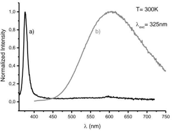
The luminescence properties of these materials were investigated. The corresponding emission graphs are reported on Figure 5. Centered at 5.1nm (0.6) Pa rtic le s nu m be r 50 nm
Figure 5. Emission spectra of ZnO nanoparticles obtained through supercritical fluid route a) and organometallic synthetic route b) under a 325 nm
excitation wavelength.
The luminescence of the nanomaterials obtained through organometallic synthesis present a visible emission. The recombination of the photogenerated electron-hole pairs leads to a wide band which is maximum at about 600 nm. The visible luminescence of ZnO is still subject of controversies. This “yellow orange” emission seems to be linked to the recombination of a shallowly trapped electron with a deeply trapped hole. In this process the photogenerated hole is first trapped by surface defects at the surface of the material. Then it migrates to vacancy levels located in the core of the particle leading to the stabilization of a deep hole trapped level. The emission takes place when the photogenerated hole trapped in the deep defect as an oxygen vacancy recombines with the photogenerated electron trapped in a shallow level located below the conduction band.
The UV excitonic is generally observed for high temperature gas phase routes because these syntheses allow the generation of high crystalline quality ZnO materials. But the control of the shape and the size of the nanostructures is difficult. The supercritical fluids route makes possible the precipitation of nano-size particles. By controlling the pressure and temperature, it is possible to avoid the stabilization of bulk or surface defects. The lack of trapping levels within the gap makes possible a direct radiative recombination of the photogenerated electron hole pair. By consequence, the resulting emission spectrum is a unique sharp peak peaking in the UV range.
Such optical properties announce significant difference of sensitivity regarding the environment of the nanoparticles and their surface activity.
CONCLUSION
As demonstrated, photoluminescence can provide a diagnostic on a material. One can play with the temperature to make a doping element migrate within a spinel structure. An evaluation of the thermal history of the compounds can be done. It is also possible to switch the response of a luminescent elpasolite under an appropriate UV excitation beam. Application such as UV detectors or data storages can be proposed by the monitoring of the emission. Finally, once the synthesis route is well-controlled, one can choose to favor UV or visible radiative de-excitation of the well-known ZnO matrix.
ACKNOWLEDGMENTS
The work was funded by the French National Agency for Research ANR AMOS program (ANR-2010-BLANC-0820), the CNRS, the LaPhIA excellence cluster program (IDEX Université de Bordeaux), the pole de compétitivité Routes de lasers® and the Conseil Régional d’Aquitaine.
REFERENCES
[1] C. Ronda, Luminescence, from theory to applications, (2008) Wiley VCH, Weinheim [2] L. Cornu, M. Gaudon, V. Jubera, J. Mater. Chem. C, 1(34), 5419-5428, 2013 [3] L. Cornu, M. Duttine, M. Gaudon, V. Jubera, J. Mater. Chem. C, 2, 9512–9522, 2014
400 450 500 550 600 650 700 750 0,0 0,2 0,4 0,6 0,8 1,0 b) Norm alized In ten sity (nm) T= 300K exc= 325nm a)
[4] J. P. Chaminade, A. Garcia, T. Gaewdang, M. Pouchard, J. Grannec, B. Jacquier, Radiat. Eff. Defects Solids, 135, 137-141, 1995 [5] L. Cornu, M. Gaudon, P. Veber, A. Villesuzanne, A. Garcia, V. Jubera, Chem. Eur. J., DOI10.1002/chem.201405784, 21, 2015 [6]Y. Roig, S. Marre, T. Cardinal, C. Aymonier, Angew. Chem. Int. Ed., 123, 12277-12280, 2011
[7] E. Ilin, S. Marre,, V Jubera, C Aymonier, J. Mater. Chem. C, 1(33), 5058-5063, 2013
[8] M.L. Kahn, T. Cardinal, B. Bousquet., M. Monge, V. Jubera, B. Chaudret, ChemPhysChem, 7(11), 2392-2397 (2006) [9] A. Glaria, M. L. Kahn, T. Cardinal, F. Senocq, V. Jubera, B. Chaudret, New J. Chem., 32, 662–669, 2008
[10] Z. Lou and J. Hao, Thin Solid Films, 450(2), 334, 2004
[11] K.H. Winbow and J. Cowley, Ceramic Engineering and Science Proceedings , 17(1), 102, 1996
[12] J. Popovic, B. Grzeta, B. Rakvin, E. Tkalcec, M. Vrankic and S. Kurajica, J Alloys Compd, 509(34), 8487, 2011 [13] R.F. Cooley and J.S. Reed, J. Am. Ceram. Soc., 55, 395, 1972
[14] J. Popovic, E. Tkalcec, B. Grzeta, S..Kurajica and B. Rakvin, Am. Mineral., 94, 771, 2009
[15] J.C. Waerenborgh, M.O. Figueiredo, J.M.P. Cabral and L.C.J. Pereira, J Solid State Chem., 111(2), 300, 1994
[16] A. LeNestour. Corrélation structure-propriétés d'absorption UV-Vis-IR associée aux états de valence du cuivre dans des oxydes à base de
zinc de type spinelle et würtzite. PhD thesis, Université Bordeaux 1, avril 2006.
[17] H. Matsui, C.-N. Xu, Y. Liu and H. Tateyama. Phys. Rev. B, 69, 235109, 2004
[18] N.J. van der Laag, M.D. Snel, P.C.M.M. Magusin and G. de With, J Eur. Ceram. Soc., 24(8), 2417, 2004 [19] M. Vasile, P. Vlazan, and N.M. Avram, J Alloys Compd, 500(2), 185, 2010
[20] L. Torkian, M.M. Amini and Z. Bahrami, J Inorg. Mater., 26(5), 550, 2011 [21] T. Koskentalo, M. Leskelä and L. Niinistö. Mater. Res. Bull., 20(3), 265, 1985
[22] A. van Die, A.C.H.I. Leenaers, W.F. van der Weg and G. Blasse, Mater. Res. Bull., 22, 781, 1987 [23] R. Mlcak and A.H. Kitai, J Lumin., 46(6), 391, 1990
[24] Cross, Ly. J.; Hillebrand, W. J. Z. Kristallogr. Mineral. 12,495, 1887 [25] Meyer, G., Progr. Solid State Chem., 14, 141, 1982
[26] Tanner, P. A., Top. Curr. Chem., 241(Transition Metal and Rare Earth Compounds III), 167-278, 2004 [27] Pedro, S. S.; Sosman, L. P.; Barthem,R. B.; Tedesco, J. C. G.; Bordallo, H. N. J. Lumin., 134, 100, 2013. [28] Andrews, L. J.; Hitelman, S. M. Ettore Majorana Int. Sci. Ser.: Phys. Sci., 30, 515, 1987
[29] Laroche, M.; Bettinelli, M.; Girard, S.; Moncorgé, R. Chem. Phys. Lett., 311(3-4), 167, 1999
[30] Yang, P.; Zhou, X.; Deng, H.; Rodriguez, M. A.; Feng, P. L.; van Loef, E. V. D.; Shah, K. S.; Doty, F. P. IEEE Trans. Nucl. Sci., 60, 1033, 2013 [31] Glodo, J.; van Loef, E.; Hawrami, R.; Higgins, W. M.; Churilov, A.; Shirwadkar, U.; Shah, K. S. IEEE Trans. Nucl. Sci., 58, 333, 2011 [32] Aull, B. F.; Jenssen, Hans P. Phys. Rev. B: Condens. Matter Mater. Phys. 1986, 34, 6647.
[33] Birowosuto, M. D.; Dorenbos, P.; van Eijk, C. W. E.; Kraemer, K. W.; Guedel, H. U.; J. Phys.: Condens. Matter., 18, 6133, 2006 [34] Buñuel, M. A.; Moine, B.; Jacquier, B.; Garcia, A.; Chaminade, J. P. J. Appl. Phys., 86, 5045, 1999
[35] A. B. Djurišić et al. Small, 2, 944, 2006 [36] C. F. Klingshirn, ChemPhysChem, 8, 782, 2007
[37] R. Hauschild, H. Priller, M. Decker, J. Brückner, H. Kalt, and C. Klingshirn, Phys. Status Solidi C, 3, 976, 2006 [38] C.H. Ahn, S.K. Mohanta, N.E. Lee and H.K. Choa, Appl. Phys. Lett., 94, 261904, 2009
[39] L. Guo , S. Yang, C. Yang , P. Yu , J. Wang , W. Ge, G. K. L. Wong,. Chem. Mater., 12, 2268, 2000 [40] C. X. Xu, X W Sun, X H Zhang, L Ke, S J Chua. Nanotechnology, 15, 856, 2004
[41] D. C. Reynolds, D. C. Look, and B. Jogai, J. Appl. Phys., 89, 6189, 2001
[42] Q. X. Zhao1, P. Klason, M. Willander, H. M. Zhong, W. Lu, J. H. Yang, Appl. Phys. Lett., 87, 211912, 2005 [43] K. Vanheusden, W. L. Warren, C. H. Seager, D. R. Tallant, J. A. Voigt, B. E. Gnade, J. Appl. Phys., 79, 7983, 1996