I Sr S A CH U S E T-N ThQA, Ti f U TKE c :LF T E C H N K L OGY i
AJ~~#ACH~JLTIJ `'' ~Elf:~; C
0-A 8.45 GHz Ga0-As FET 0-Amplifier
Alain Charles Louis Briancon
Technical Report 499 May 1983
/
6,pj
O
/y
Massachusetts Institute of Technology Research Laboratory of Electronics
Cambridge, Massachusetts 02139
This work has been supported by the National Aeronautics and Space Administration under Grant NAS8-34545.
-A 8.45 GHZ G-A-AS FET -AMPLIFEER
by
Alain QCarles Louis Briancon
Submitted to the Deparnent of Eeical Engineering and Computer Science,
May, 1983, in partal fufillent o the requirnets for the degrees of
Master of Science and of E Engineer.
ABSMAC
Procedures for measuring power scattering and noise parameters of Galium-Arsenide fieldeffect transistors in the X-band are presented. The variaions of the noise parameters and of various gains a particular FET with frequency, the device's physical temperanre and DC bias are reported. The physi parameters of the FEl's channel are determined.
Details of the design, construction and evaluation of two single stage amplifiers operating at 8.45 GHz are presented. Both are tuned using micr ip boards. At 8.5 GHz and room temperature, the first prototype exhibits a 6.8 dB gain and a noise temperature of 160 K at 8.5 GHz and room temperature. Deformations of the micrstip boards, when cooled, prevent the operation of the ampfier at cryogenic tenperatures. The second prototype, when cooled at 77 K, exh a 7.2 dB gain and a noistemperature of 68 (an iprovement factor of 2.6 over the noise performance at 293 K). This study is part of the development of low noise,
cryogeni-cally cooled X-band FET amplifiers for VLBI observations in space.
Thesis Supervisor: Bernard F. Burke.
Tide: Wiiam A. M. Burden Professor of Astrophysics
_ __
3
A Eva et Maria
.__. _1__1_·________1__·I 111-_11111·_1 1 1.
A quatre heures du matin, l'dtd, Le somme l d'amour dure encore. Sous les bosquets l'aube dvapore L'odeur du soir ft.
Mais bas das 'immense cantier Vets le soi des Hesprides,
En bras de chemise, les charpeters D*j safit'nt
Dans leur ddert de mousse, anquiles, Ils prparent les lambris prdceux
O la riches de dla ve Rira sous de faux cieux.
Ah! pour ces Ouvriers harmant Sujes dun roi de Babylone, V*nus! LaIse un peu les amants,
Dont l'ime es en couronne. 0 Reine des Bergers!
Porte aux travaeurs l'eau-de-ve, Pour que leurs forces soient en paix En andant le bain dans la mer, a midi.
Arthur Rimbaud
ACKNOWLEDGEMENTS
I would like to thank all the people who cooperated in tis thesis. Frs, I would like to cxpress my gratude to Professor Bernard F. Burke for his support and confidence. I would also like to thank Professor Robert. L Kyhl for introducing the subject and our discussions on the topic.
A well deserved thanks is given to all the mebers of the
MlT
radio-astronomy group for helping with the hardware and equi nt, aswerng my interrogaions and creating anenjoy-able working aDsphere. Doctor (o be) Barry R. Allen must be acknowledged for the hours he spent introdudng me to microwave FET's and for solving my problems. I would like to thank my ofmate Vivek Dhawan for the many stimuain g conversation s we had.
Part of my funding was furnished by ThomsonCSF Division Equipements Avioniques Departement RCM. I am indebted to them and Sir Caude Rouard for their support.
I expres my warmest thanks to my parents and fmily for their encouragement, under-standing and support, for their love and the long periods they endured away from their son and brother.
Finally, I express my gratitude to my wife (to be) Maria for all her help in reviewing and proofrcaing this thesis. It is a blessing to be close to someone who provides so much love and moral support
6 Table of Contents ABSIRACT 2 ACKNOWLEDGEMENTS 5 TABLE OF CONTENTS 6 CHAPTER I: INTRODUCTION
1: Low noise receiver for radio astronomy 8
2: Objetives 9
3: The rsearch 10
4: References 11
CHAPITER II: THE FELD-EFFECT TRANSSTOR
1: Field-Effect Transistor Struce 12
2: Eleton mobility in Gallium-Arsenide 13
3: FET operation 17
4: FET DC characterstics and small signal rcuit 19
5: Ncise theory of the FET 24
6: FET noise representations 29
7: References
CHAFPTER : FET PARAMETERS
1: Scattering parameters 33
2: Gain and stability 38
3: Noise parameters 44
4: DC characteristic and internal elements 59
5: References
CHAPTER IV: FET SINGLE STAGE AMPLIFIR
1: Purpose 65 2: Design 66 3: First prototype 72 4: Second prototrpe 76 5: References 83 CHAPTER V: CONCLUSIONS 1: Result 84
7
APPENDIX Cl: NOSE PARAMETERS DETERENATION
APPENDIX C2: NOISE TEhPERATURE MEASUREMENTS
APPENDIX C3: LOSSES IN MATCHING NETWORKS
87
89
101
·1^-·I·---CHAPTER I: INTRODUCTION
1. Low noise receiver for Radio Astronomy
The purpose of a radio astronomy receiver is to detect and amplify signals received by the antenna from celestial radio sources. The power received is very low, varying from 10- 20 Watt for a spectra line observation to 10-iS Watt [1 for a
contn-uum observation. In most cases, the emissions consist of incoherent radiations as is the noise generated by the receiver itsef. The requisites for a radio astronomy receiver are thus low noise and high stability. High stability is needed so that the input signal can be integrated and variations in the radiated power detected. Another requirement for an accurate reproduon of spectral observations is that the receiver be linear in output
Most radio astronomy receivers operating under 15 GHz are superheterodyne. The input signal is amplified by a low noise amplifier, then converted to a lower fre-quency by. mixing it with a local oscillator. The noise characteristics of this type of receiver are determined by the front end amplifier.
I
Although they are not as performant as cooled maser-upconverted systems, cooled
Gallium-Arsenide
Field Effect tansistor amplifiers tend to be used with increasing fre-quency. These amplifiers present several advantages as compeaion for their poorer performances Input and output drcuits are less critical to design than that for a nega-tive resistance amplifir. The power is supplied through low DC voltages and not through power oscillators in the amplifier. Fnally, ming circuits are realized t the operating freq ncy.2. Objectives
Projects of VLBI observaions in space [2,3 ] reqire X band (8-12.4 GHz) low noise amplifiers. In this frequency range, the properties of low noise GaAs FET's have not been studied in detail, particulartly at low teperatures. After several attempts, an FET (NEC 13783) was chosen for its performance at room temperature. The
proper-ties of the FET measured at both 77f and 300 and between 8 GHz and 10 GHz
are reorted. The power scattering and nois parameters of this transistor are calcu-lated. A single stage amplifier is constucted. Using these data, attempts are made to answer the following questions:
Can the FET's performance at 77 K be inferred from its performance at 300 K?
How do the noise parameters of the FET vary with temperature and frequency? How does the FE1r DC bias influence its noise and scattering parameters?
Is the circit design for an amplifier operating at cryogenic temperature different from that of an amplifier operating at room temperature?
What problems and limitations are inherent to operation at cryogenic temperature?
3. The research
The work described herein was carried out at the M1T radio astronomy group laboratory.
Chapter II contains a brief summary of the properties of Gallium Arsenide and of GaAs Field Effect tanssos. Microwave behavior of the FET and the currently admitted noise theory of the FET are presented. The i noise representations of
a twoport and how they relate to each other are also introduced.
Coapter m presents the measurement techniques and the measured scattering parameters. From the experimental data, stability and gain are computed. The noise parameters ar determined and their variations with frequency, temperature and DC'
bias examined. The tempratre dependence of the FETs DC characteristics and of several internl parameters is studied.
Chapter IV presents the design and performances of two single stage amplifiers at both room and cryogenic temperature. Conclusions are then drawn about microstrip tuning networks.
Chapter V summarizes the research and suggests further work in the field.
-References
1. J.D. Kraus, Radio Aasronomy, McGraw-hill Book Cmpay (1966).
2. B.F. Burke, "Radio Antennas in Space: The next 30 Years," MIT Radio
Astrron-omy Contributions 4 (1982).
3. R.A. Preston, B.F. Burke, R. Doxsey, J.F. Jordan, S.H. Morgan, D.H. Roberts, and LL Shapiro, 'The Future of VLBI Observatories in Space," MIT Radio
Astonomy Contributions 5 (1982).
CHAPTER II: THE FIELD-EFFECT TRANSISTOR
1. Field Effect Transistor Structure
Field-effect trasistors offer many features for application in cryogenic microwave amplifiers. They have a higher input impedance than bipolar transistors that allows easier matching to microwave system. They are majority-carrier devices and conse-quently can be operated at higher frequencies and lower temperatures [1 ]. A typical stucture of FET is shown in Figure II.1.
A thin epitxial layer of thickness in the range 0.1-0.5 pmn is grown over a semi-insulating Gallium-Arsenide substrate. The substrate has a resistivity greater than 107 fcm and the layer of typically 10- 2 fcm. Above the etaxial layer are located
three metal electrodes. This structure is approximately 300 m wide and is reasonably modeled as two dimensionaL
Best noise results [ 2 ] of such FETs are achieved with a high doping level in the
a layer, typically 1017 cm 3. This doping is usually realized with selenium impurities.
One is also required to have the smallest possible gate and source metal resistances.
Sc alloyed ohmic contact ___L __ _ -Scnoteky rectyin connection n type doping'
epitaxial layer semi-insulating
Gallium-Ar senide
Figure . 1
FET Structure
This is realized by localized heavy doping (109 cm-3 ) under the electrodes. A short
gate length is also needed; recent improvements in the fabrication allow a gate length of
typcally 0.5 mn.
An important characteristic of Gallium-Arsenide is its non-ohmic behavior for fields greater than 3 kV/cm. Let us consider a microwave FET of gate length 1 um.
A voltage drop of1 V acrs this gate correspond to an average field of 10 kV/cm. One must take the field dependence of the electons' mobility into account in order to understand the operation of the FET.
2. Electron mobility in Gallium-Arsenide
The conduction band of the GaAs as presented in Figure 11.2 has a central minimum at 1.43 eV and a saiellite minimum at 1.79 eV; the two of them consist of
r-r
_AOM I I - -Ooe i i j~~~~~~~~~~~~~ nr in. °fclvalleys with local minima of potential energy [ 1 ]. E Energy 1.43 1111 I Satellite valley 1.79 eV k [C00] & vector les Figure 11. 2
Energy -Band Struczure of Gallium -Arsenide
Rees [ 3 has calculated the electron velocity versus the applied electric field for the two valleys. These results are plotted in Figure 1I.3.
ley
ocity xl1O cm/sec
I
zc
central valley velocityElectric
field in kV/cm Vs Satellite valley velocit s fraction of electrons in the satelli V s (l-Os)Vs c total velocity Figurwe II. 3
Carrer DrFi Veocjry vers Electic Field for High Puriy Gallium -Arsenide For low fields, below 2
kV/cm, all the electrons
are in he centra valley ( =0). As the field increases Conduction
Iecrons end to transfer t the satele valey The life time of the eecons
in this valley is only 1.8
pcosecods and they tend to return to
-.---____1_11··111II__
the central valley. This travel of electrons back and forth between the two valleys will contribute to the noise of the FET. But, as the electic field increases, the time aver-. age fraction of electrons in the satelli valley also increases. For a field of 15 kV/cm, nearly 75 % of the conduction etrons are in the satellite valley. In the central valley, the mobility of an electroi is about 8500 cm2/s and its effective mass 0.068 m0,
where m0 is the mass of the free electron. Higher effective mass in the satellite valley (1.2 mo) reduces its mobility to about 100 cm2/Vs. Electrons of the satellite valley
essentially do not contribute to the conduction process. At low fields, the mobility is approximately constant, the velocity and therefore the current are almost linear. As the field increases, the current no longer obeys the linear relationship. At 3 kV/cm the transfer of electrons becomes significant. The current reaches a maximum for a field
of 4 kV/cm. Higher fields up to 20 kV/cm cause the current to decrease and yield a
negative differential mobility.
The saturation in velocity for carriers (electrons) in the central valley for. fields greater than E =4 kV/cm ca be explained as follows. For fields greater than E, electrons have an energy comparable to the energy of an optical phonon; an increase in the electric field causes energy to trander to the lattice and not to the carriers.
Rees also studied the way electrons respond to a transient field applied over the DC value when a sudden change in the field is applied. That is, carriers in the satellite valley reach equilibrium faster than the carriers in the central valley (0.1 picoseconds versus 5 picoseconds). This is more visible if the transient field applied is higher than
4 kY/cm [ 4 ]. As the electric field is applied, a time period of approximately
picoseconds passes before electrons are transferred from the central to the satellite
ley. During that period, they remain in a igh mobility state and therefore acquire a high velodity. This total drift exceds the steady state velocity they reach at equilibrium by more than a factor of 2. This effect is nevertheless only noeable for FEI's with a gate length less than 3 pam, which is the case for most recent FET's.
3. FET operation
During normal operation, the FE1 has a positive drain and a negative gate tension with respect to the source. It priniple of operation is epained in Figure 11.4 [4 ]. A depletion region without carries is formed under the gate. This acts as an isolator and the eletons are conswained to flow through the channel so created. The height of the depletion region depends on both the applied gate to source and the drain to source voltages. The fluctuation of the tension Vs that modulates the height of the channel also modulate its resistance and the drain current. This is the amplification mechanism of the FET.
Proceeding from the source to the drain, the depletion region becomes larger, the channel narrower. To compensate for this decrease in the channel cross section, the electric field and the velocity of the electrons increase. As the electric field increases, the electrons tend to transfer to the satellite valley. Himworth showed [5 that the velocity rises to a peak at x then falls to a saturated value under the gate. The height of the conducing channel in this saturated region is approximately consrant. This rela-tively slow movement of carriers under a high electric field, in order to maintain the drain current, requires a heavy electron accumulation. Between x2 and x3 (see Figure
II.4) exactly the opposite phenomenon occurs. That is, the channel widens and the electrons move faster as they regain the central valley.
Source Electric field 4 kV/cm Electron velocity Space :harge on region Figure . 4
Channel Cross -Section, Electric Field, Electron Drift Velocity and Space Charge Distribuion of GaAs FET
This analysis does not take into account the non equilibrium phenomenon described by Rees that allows the electrons to exceed the peak equilibrium velcdty, a phenomenon that occurs for gates less than 3 rlm long. This effect increases the
__
velocity at point xl by a facr lose to 2 and decreases the velocity at x3 by a factor of 1.5. Globally, it shortens the transit time of the electron within the "saturated' region.
This phenomenon is paricularly visible for a gate lengh less than 1 wn.
Although it has been shown that this model gives an approximate behavior for small gate lengths, it does not permit an analtical treatment.
4. FET DC characteristics and small signal circuit
It is posible to desnibe the FET behavior using a lumped element network for frequencies up to 12 GEz. Several authors have esamined this problem. Currenty, the commonly accepted reference work is a paper by Pucel, Statz and Haus [6 ], which also develops the noise characteristics of the Gallium-Arsenide Field Effect Transistor.
The simplified model Pucel et aL used is ilhustrated in Figure 11.5 and Figure II.6.
Source Gate Drain
L = L
o 1
3
LFigure 11. 5
Idealized Geometry of a Field Effect Transistor
The FET is broken into two parts. The region I close to the source is of ohmic
V
S
Velocity
Esat
Figure 11. 6
Piece Linear Simpl4ed Velocity
versus Electric Field Relationship
conductivity and the carriers have a linear velocity with respect to the elecric field. For applied voltages exceeding the so called "pinch-off value", the longitudinal electric field will exceed the saturation field (taken to be 3 kV/cm) at point L 1. Beyond this
pinch-ff point, carriers drift at a constant veodty V, while the field due to the free
charges on the drain electode continues to increase, thus assuring that electrons remain within a saturated drift. The position of the pinch-off point and the height of the channel in the saturated region are functions of both gate to source and drain to source voltages.
Using this model Pucel et aL obtained a DC characteristic for a Field-Effect Transistor as presented in Figure I1.7. The dotted line marks the limit between DC
1*'
Lge VDS (v)
Figure I. 7
FET DC Characterisic
bias where the FET works only in ohmic conducivity (at the left of the line) and DC bias where high fields create a velocity saturated region under the gate. The charac-teristics Pce et aL derived from their model match well with DC characcharac-teristics of
aual FETs [7,8 ], [ section
IV.3].
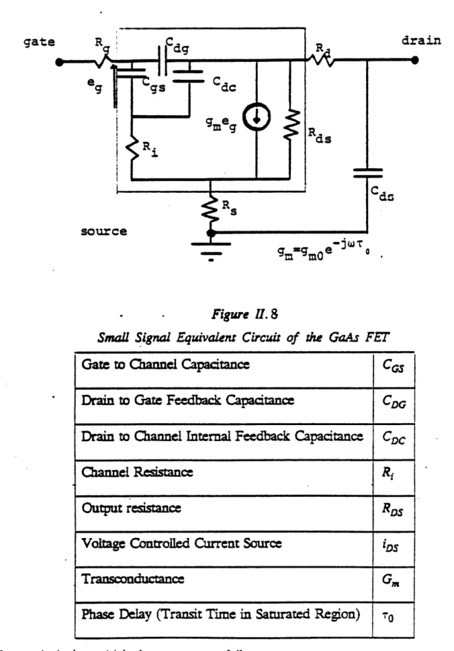
This model also provides an equivalent circuit for operation in the common source configuration. Figure I.8 presents the racit while Figure I.9 shows the physical ori-gin of the circuit elements. The intrinsic elements of the circuit are as follows:
___ ---1111__11 ___ n~~~~~~
gate
g=gmo e
-Figure II. 8
Small Signal Equivalent Circuit of the GaAs FET
Gate to Cannel Capacitance CGS
Drain to Gate Feedback Capactance CDG
Drain to Channel Internal Fedback Capacitance CDC
Channel ResstancR i
Output resistance R
Voltage Controlled Current Source ZiD
Transcnductance G
Phase Delay (Transit Time in Saturated Region)
o
The ex=insic (parasitic) elements are as follows:
_ --- -__-_
Source Gate Drain _ . _ -ds Figure Physical Origin of 11.9 Circuit Elements Sutrate Capacitanc C
at metal and Spreading Resistance R
Drain to Source plus Contact R tance Rd
Source to Channel pnlus Cont Resistance R,
It is possible by using this model and the geometry of the FET to determine the frequency limitations of such a device. Let r be the input to output resistance rato
r= R8 +Ri +R s
Rt
let r be the feedback gate time constant
= 2'Rg Cdg
fT the frequency at which the current gain is unity is given by
1 gm
fT 2-:r C
2 c,
The unity gain frequency (also referred as the nmaimum lation frequency) is
fS=
Decreasing L the length of the gate decreases the gate to channel capacitance and
increases the transconductanct. One can also express the current unity gain frequency as a function of the gate length, acording to [9]
ft.- 2zrL
where v is the effective velocity during the crosing of the gate, i.e average of the drift velocity of the carrier over the gate length. For small gate length, va is approxi-mately independent of and fr varies as 1L . To have a high fr and therefore a high frequency f,, one needs a short gate and a high velodty carrier. In silicon and Gallium-Arsenide, electrons have a higher mobility than holes; in GaAs, electrons have a six time larger mobility and a two .time larger peak drift velocity than in the silicon. This is why only n channel GaAs FETs are used for microwaves applications.
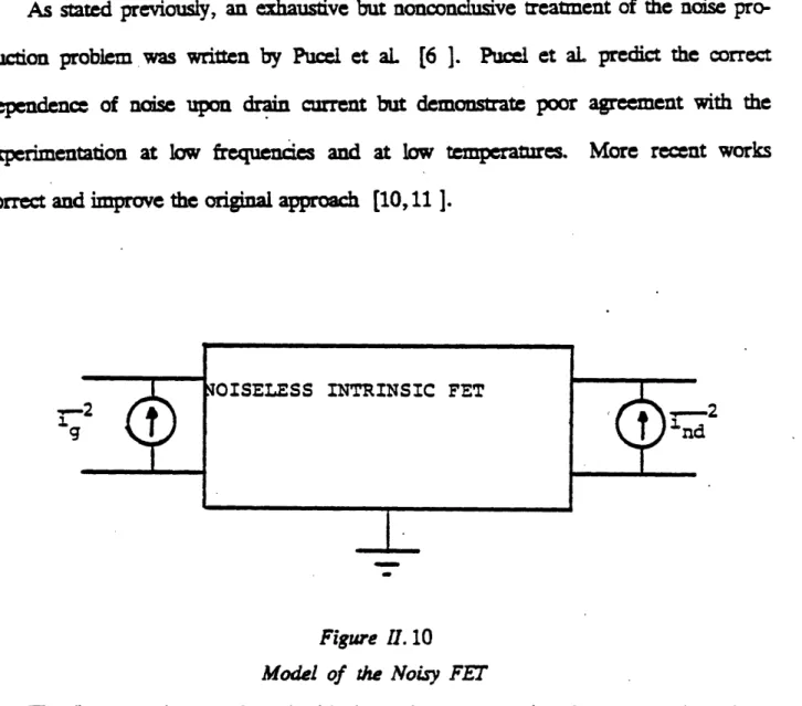
5. Noise theory of the FET
The complete description of the noise properties of the Gallium-Arsenide FET is an intricate problem mainly due to the involvement of noise production. In general, the phenomenon involved in the production of noise are both frequency and tempera-ture dependent, dependences that are not always well understood.
As stated previously, an exhaustive but nonconclusive treatment of the noise pro-duction problem was written by Pucel et aL [6 ]. Pucel et aL predict the correct dependence of noise upon drain current but demonstrate poor agreement with the
experimentation at low frequencies and at low temperatres. More recent works
correct and improve the original approah [10,11 1.
Figure II. 10 Model of the Noisy FET
The first stage is to analyze the ideal transistor, postponing the computation of the noise contribution due to the parastics elements. The equivalent circuit for the ideal FET is shown inside the dotted line box in Figure I.8. The noisy transistor can be represented by using two noise current sources, one at the input and one at the output as shown in Figure L. 10.
Basically, the noise current of the input represents a Johnson type noise in the channel region which is emphasized by hot electrons in the channel. This noise voltage also causes noisy fluctuations in the depletion layer height. This results in the creation of electric dipoles drifing through the saturated region. The output noise source
---represents these dipoles drifting to the drain contact.
The two noise currents id and i,, are caused by the same noise voltage in the channel and are therefore correlated. The correlation coefficient is defined as
iC=
7where j =/ - 1. The correlation jC is purely imanar cause noise sources in the drain and in the gate circuits are capactively coupled. The theory of Pucel et aL per-mits the lation of ,i an d C.
One has to consider separately the two regions of the channel labeled I and in Figure H.S. In a previous work Baetchold showed [12 that in the Gallium-Arsenide,
the measured noise temperature electric field curve can be fitted by
TTO=1+ 8 (E,
J,
where To is the physical temperature of the lattice, ES is the saturation field and 8 is an empirical coefficient equal to 6. Using this relationship and the longitudinal depen-dence of the electric field, Pucel et aL computed for each point of the unsaturated region (region I) the Johnson noise contribution. Integrating over the whole region I, one can compute the induced gate noise current i .
In the saturated region, we cannot describe the noise as a Johnson noise. The noise current is interpreted as a distribution of spacialy uncorrelated impulses. Each of these impulses results in a displacement of a charge and produces a dipole. The dipole is created within a saturated velocity region and is thus unable to relax. The dipoles so created then drift unchanged to the drain contact where the drain noise current i2 can
be calcated. Through capacitive coupling the noise production in region I will contri-bute to the noise current on the drain and vice-versa. These contributions are summar-ized in the overall correlation coeffient jC.
The mean square time average of i and of i can be ex d by [12 4kT AfgP
i4:- 4kT Af w2C2,RIg.
where k is the Boltm ann conStant TO the lattice temperature, Af the bandwidth,
the angular frequency, C., the gate to source capacitance, g the magnitude of the low frequency transcndutance, P and R both dimensionless factors dependent on the device geometry and on the DC bias.
The cxrinsic resistances R, and R generate thermal noise themselves and degrade the noise performance of the FET. The equivalent circuit model for the FET which includes the noisy parasitics is shown in Figure 11..
One can express the minimum noise figure (see section 1.6) of the intrinsic FET as a function of the parameters R, P and C. Under the assumption f<<fr ( This is usually the case; a typical value of fT is 90 GHz ), we have
F,~n1+2 PR 1-C2)f.
We can have for short gate length a correlation coefficient close to one in magnitude and a substantal noise cancellation, corresponding to a desucive interference of the two noise currents.
The above expression predicts for low frequencies an almost linear dependence of
~--eg 4kTORgAf -7 ea rain source Figure I. 11
Equivalent Circuit for Noise Calculations
the minimum noise figure with frequency. Such a decline was not observed. Recent works at low temperatures [13,14 ] revealed a disagreement between Pucel et al.'s results and the experiment.
Several explnnatons were advanced to agree with experimental results. Pucel et al proposed a trap theory with traps at the epitaxial layer substate interface. But the temperature dependence of the trap theory was found to differ from the experiment. Another explanation was that of the intervalley scattering noise [15 ]. The intervalley scattering noise is a weak function of the physical temperature of the lattice and thus
can be a significant contribution at low temperatures.
A different approach of the problem is proposed by Graffeuil [16 ] who considers the electron noise temperature to be both elecic field and frequency dependent. Using this model, he succeeds to match theory and practice well More recently, Brookes [ 11 ] reonsidered the Pucel et a's origina approac pplyapping it to a channel whose thickness is not constant but modeled as a gaussan random variable. Even when the variations of the channel height are small compared to its mean value, he matches low frequency noise figure data.
6. FET Noise Representations
The noise figure of a twoport device is defined as the ratio of the noise of the
out-put of the two port driven by a noise source to the noise of the outout-put of the same
twoport idealized (niseless) when driven by the same noise source.
The noise source used to compute the noise figure F is an impedance Z com-bined with its associated equivalent thermal noise source as described in Figure IL .11. Using the expression for the noise generators of the FET it is possible to show [17 ]
that the noise figure can be written as
F=1+ R [rn+gn Z,+z ]
where Z, =R, +jX is the source resistance and r. ,gn ,Z, three intermediate parameters whose theoretical values can be derived from the Pucel theory [6 ]. Z is known as the noise correlation impedance. F is a minimum when Z, is at an optimum, ie
ROW [e (Z.) gn |
XOp-Im (Zc)
Expressed directly as a function of P, R, C and fr the value of F at the mininum is
Fm _ f +2mRP(1
(l+2-
2Another representation of the noise behavior of the device is its equivalent noise
tem-perature. This is related to the noise figure by the relation
T-To (F-I)
where To is equal to 290 K
Any noisy two ports noise temperature can be represented by four parameters: the minimum noise tmperature Ti, the optimum source impdance Zo = Ro +JX
and the noise conducance gn [17 ].
The noise temperature as a function of the source impedance Z =R +X is given
by
Tn=Tsin+TO R [(R-Ro) + ( -Xopt) 2
]
The relation between the two representations is known as the Rothe-Dalke relations
R, =gn Z.,,,
Tain 1
R = T ' 2gn -R°
XC -- -Xopt r,, gn (Rt -R )
The relations developed in this chapter form the basis for interpreting the experimental results.
References
1. Sze, pp. 7-60 in Physics of Semiconductors Devices, Wiley Interscience (1982).
2. M. Ogawa, K. Ohata, T. Furutuka, and N. Kowamura, "Submicron Single Gate and Dual Gate GaAs MESFErs with Improved Low Noise and High Perfor-mance," IE Transactions on Microwave Tory and Techniques ,TT-24,
pp.300-304 (June 1976).
.3. H.D. Rees, 'Tme Response of the High Field Di fibutian in GaAs," IBMJ RES. Develop. 13, pp.537-542 (September 1969).
4. CA. Liechti, "Microwave Field Effect Transistor -1976," M77.24, pp.279-300 (June 1976).
5. B. Himysworth, "A Two-dimensional Analysis of Gallium Arsenide Junction Field
Effect Transistor with Long and Short Channels," Solid Stae Electron. 15, pp.1353-1361 (Decber 1982).
6. H. Statz, H. Haus, and R. Pucel, "Noise Chraterics of Gallium Arsenide Field Effect transistors," IEEE Transactions on Electron Devices ED-19, pp.674-680 (May 1974).
7. Alpha industie, ALPHA 3003 Data Sheet, August 1981.
8. Nippon Electronic Company, NEC 13783 Data Sheet, August 1980.
9. T. Maloney and J. Frey, "Frequency limits of GaAs and InP Field Effect Transis-tors ," IEFF Transactions on Electron Devices ED-20, pp.357-358 (June 1975). 10. S. Weinreb, "Low-Noise Cooled GaAsFET Amplifiers," IEEE Transactions on
Microwave Theory and Techniques MTT-28, pp.1041-1054 (October 1980).
11. T.M. Brookes, "Noise in GaAs FET's with a Non Uniform Channel thickness," IEEE Transactions on Electron Devices ED-29, pp.1632-1634 (October 1982).
12. V. Baetchold, "Nois Behavior of Schottky Barrier Gate Field Effect at Microwave Frequencies," IEEE Transactions on Electron Devices ED-19, pp.674-680 (May 1972).
13. G. Tomasetti, S. Weinreb, and K. Wellington, "Low Noise 10.7 GHz Cooled Amplifier," Elctronic Journal, NRAO (November 1981).
14. S. Weinreb, "Low Noise Cooled GaAs FET ," Electronic Journal, NRAO (April 1980).
15. Barry R Allen, "A 43 GHz cooled mixer with GaAs FET IF," MIT (August 1979).
16. J. Graffeuil, "Static, dynamic, and noise properties of GaAs Mesfets," Universie Paul Sabatier.
CHAPTER
II:
FET PARAMETERS1. Scattering parameters
At microwave frequenies, the only quantities directly measurable are the ampli-tude and phase angle of propagating waves. If one considers an N port device [ 1 , at each of its ports, part of the input wave is reflected and part is transitted (scattered) to other ports. If we denote with a' the vector composed of the incident wave ampli-tudes and b the vector composed of the emanating wave ampiampli-tudes, the relation between a and b for a linear device is:
b=Sa
where S is the power scattering matrix. In the case of the FET, this S matrix is com-posed of only four parameters. These parameters are in general complex and thus
require, for the phase term one or more reference planes for the phase term.
Manufacturers usually provide the value of the various scattering parameters without indicating the plane they are referenced to. This causes a problem when using these specifications at high frequencies where small physical distances can create large phase shifts.
Measurement Techniques
Two different FETs from different man ers (NECALPHA) were chosen to be studied and used in a cryogenically cooled amplifier; table 11.1 presents the two manufactrers' ncim [ 2,3 ].
at 8 GHz Table fll. 1
The ALPHA MESFET was found to oscillate around 3.5 GHz for a large variety of source impedances when biased with a drain current of 30 mA and was therefore disre-garded for the use in the amplifier. Its scattering parameters were not even measured.
The scattering parameters of the NEC FET were measured using the rest fixture described in Figure IL 1. The test fixture does not allow the biasing of the transistor, thus avoiding the creation of parasitic elements due to DC bias networks. The task of biasing the FET was performed by two bias Tee networks (HP 11590A). They were found to be negligeably lossy over the frequency range of measurements. Two dif-ferent kinds of connectors were used to connect the dilectric board to the network analyzer used for the measurements. The APC-7 standard was used at room tempera-ture to obtain a better accuracy and an overall lower VSWR; heat links were avoided by using the OSM standard at cryogenic temperatures. The fixture's microsip has a characteristic impedance of 50 and lies on a teflon fiberglass board.
FET F G
ALPHA 3003 1.5 dB 14 dB
NEC 13783 1.2 dB 11 dB
I
I
l
I
Figure II. 1
Test Fixture Used for Scattering Parameter measurements
A teflon cylinder was placed over the device and held firmly against the board with a spring like piece of copper (see Figure IIL1). Between 8 and 10 GHz, the teflon cylinder created a phase shift of less than 2 degrees and an amplitude change less than .15 dB (<2 %). The gap between the input and the output boards was designed to exactly fit the FET package, so as to reduce phase errors due to positioning. These were limited to about 5 degrees at 8 GHz and 7 degrees at 10 GHz. The gap between the two source pads was equalized to that of the experimental amplifier. In order to
limit parasitic capacitance between gate and source, the ground plane under the transis-tor was milled down [4 ].
To set the reference in the measurement of dme S parameters, a 2 mils thick flex-ible piece of copper was positioned at the edge of the board and folded over the source pad. A small drop of solder provided the connection with the microstip. This set the reference planes for the S, at the edges of the FET package. For the measurements of the Sij parameters, a piece of copper with the width and thickne of the FET drain pin was held over the gap with the teflon cylinder. The Sij parameters were therefore referenced to the center of the package.
To correct for the phase shift over the FETs package, a careful measurement of the electrical length of the copper pin was made. The phase of the reflexion for shorts placed on both sides of the gap were measured and the electric length was determined ( see Figure 1m2).
LoJ
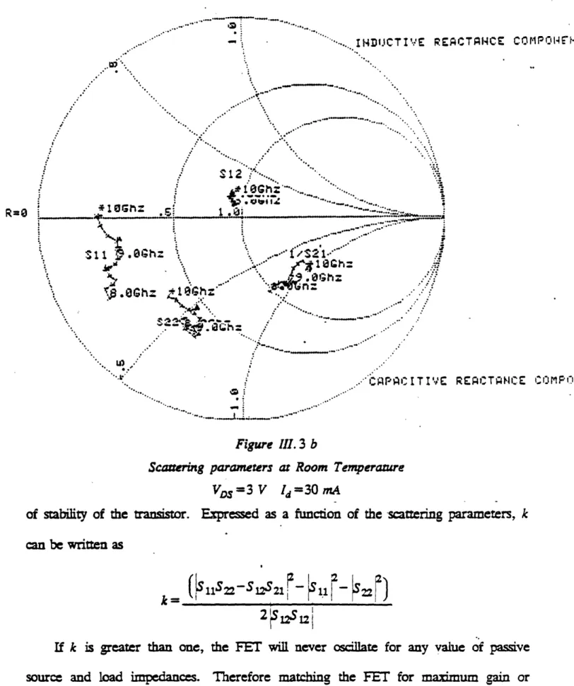
All the parameters were measured using a Hewlett-Packard network analyzer. The different scattering parameters were measured for a VDS of 3 V and a drain current of both 10 mA and 30 mA to compare with the mnnufactrer's sptLficatons. Twenty one measurement points were taken over the frequency range of 8 to 10 GHz in order to use the available computer routines. The Figures III. 3 a and 11. 3 b present a typical scattering parameter measurement at room temperature.
The reflexion coefficient magitde agreed within 10% of the specifications of the constructor, the phase was off by 25 degrees for S 11 and by a factor ranging from 30 to
short W _
i i
short I_ (Pap 2 Figure 111. 2 Phase Measuremens40 degrees for S2. A shift of 20 degrees corresponds (using an approximate theoreti-cal description of the FET case) to the phase difference between the edge and the center of the FET package. Stresses introduced as the result of the cryogenic cooling displaced the microstrip off the board. This caused the dispersion in the phase shift of S22. The remaining phase difference is most probably due to the measurement errors.
One can conclude from these results that the manufacturer takes the center of the package as the reference plane for the scattering parameters.
Transmission coefficient magnitudes were found for different FET's varying between 10% from the manufacturer specifications. This kind of dispersion was predictable for the tansducer gain S21 but was not expected for S
2.
The phase of S21 was found usually within 10 degrees of the claimed values. In addition S12 was found to be off by a factor of 90 degrees for one FET and by 10 to 30 degrees for the others.'"
I
i I I~~~~~~~~
.u.
%°.U.E ETCQ.MC4T
-" ... IHDUCTI ' RECTANHCE COrlP:,I4E.T
;'-*. .. - *. **. ..* . · · ~~ -*. . 5 .. .... : , .. .. -.. . '.% . .. . , -.. o; .. *.; .' . C ., .. . .. .- .-. ' S12 ./- ... * *.21L
...
::....
A '= r*1trG- 5' .1; : REACTAtlCE: CO,1MPO4EtIT Figure III. 3 aScattering Parameters at Room Temperature
Vs=3 V Id=lOmA
Different measurements for the same FE provided results within 10 degrees. One possible explanation for this discrepancy is that the low level of the output signal does
not allow the network analyzer to phaselock it.
2. Gain and Stability
From the measured power scattering parameters, one can determine the oscillation conditions and the different gains associated with the FET. The invariant stability fac-tor k introduced first by Rollet [ 5 is the simplest way to uniquely describe the degree
rrrrrr·r·rr·- ·---· r·iiwri··rrrr ---iri··-· ·-- - · r·r·wC -·U---- -- - -- --- I .L-6 .. . I i
- .... INDUCTIVE REACTANCE COMPcOLHN4 S 1 1 :. ·hz I .eGhz Z1.Bh a .·· '~~~~~~~~~~~~~~~~~~~~~~~~~~~3 · ·'· ~4. e ,... N.,,imt~~~~~~~", . ,.° .. 'o 1-'S21*<~~~°°'°. · · .,··. .' . ~~ *~ ~ · ':~ ~
:
' ':o -:.- *.' *... .. ; : ... *, ..- : 12.-- .,..*- . '°',* .. ~. *, , * ot ~~~~.,t - ... ~~~~.. .' 9h,h... . -*: - , 12 .: ... n_ ', . : . ''''' -* '' : : ~~~~~~~~~~~~~~~~....- · ....' . :. ; ';~
~ ~~..f
/2rr
Ieh
...
... " i 5~~~~~.. ' '- ... '"' · ~~~ . , ;z....:'/S 1·' ~ ! O·hz : ~ff~h'~ :x,,. ~~~~~~~~~~~~~~~.. . ··~ ~ ~ ~~~~~~~~~~~~.. · " . . .. o.,,.. ,i- '"'. ~~~~d · ,mki 4 .* .'' . a . * If -. '; .. iCAPC ITIV''E RECTICIE
... ss. .. . '.'
Figure III. 3 b
Scattering parameters at Room Temperature
VDS=3V Id=3 0 A
of stability of the ansistor. Expressed as a function of the scattering parameters, k can be written as
k (illS22-s2S~l m 1 I i1 i 5
212S21
If k is greater than one, the FEl will never oscillate for any value of passive source and load impedances. Therefore matching the FET for maximum gain or minimum noise can be done without restriction. The mamum available power gain
: O M P I-I f H / J R=O : i :: I I ... . ---· - ---... ..-~W U 'Z. ... ..
I ._td0
* .4 Q e *#0
. aa 8 .8 % .88 :3. .Ase..Fez
Figure 111. 4
NEC 13783 Stabilizy Factor
Ga is obtained when the input and output are matched to their respective conjugates. In terms of the stability factor
$ ' 21 2 (-The greater k, the more stable the transistr.
If k is less than one, certain passive source or load impedances will create unstabil-ity and cause the transistor to oscillate. In the input and output planes, these unstable
regions are inside circles [6 ] whose centers and radii are direct functions of the scatter-ing parameters. The maximum stable power gain G., is obtained by padding the input and output of the FET with lossy elements so that the overall twoport is unconditionally stable [5 ]. In terms of the S parameters,
a Cs Aft
t .6 14
GS = S211
The measurement of the scarin parameters at cryogenic temperature requires the use of ong semi-rigid cables to hold the test fiture in liquid nyogen. These cables present an ectr length of several tens of a wavelength whose exact value depends on the shape of these cables. This lecical length problem prevents any
accu-rate measurement of the phase of the scattering parameters.
Because the phase of the scattering parameters was not measured at cryogenic temperature, the computations of k, G, and/or G,, were performed only at room temperature. DB I . V ;3V . . . : ' : 3 ·, %-J .... ... ... ... . . .. F ... ·I I10MA-~~ L... . ... ... ... ... . ... .. ... ... ... ... i . .. .. . ... i i . ... i .... ,. . . . .... . 3 .4'JS6 S a, le J3:0 ; 1 3 Figure I. 5
NEC 13783 Maximum Available Gain
The Figure m.4 presents a typical plot of the variation of the stability factor k
*J, b
with frequency for a drain current of both 10 mA and 30 mA. The stability factor is
lower for a bias of 30 mA, principally because of the increase in the magnitude of S2 1.
Errors in the determination of the S parameters yield inaccuries in the computation of the k factor. 52 and S2 are the two parameters most subject to measurement errors (10%o) and this resuls in an error bound of ± 15% for k. Between 8 and 10 GHz, the NEC 13783 has a stability factor close to one and this 15% error bound puts
it at the threshold of being conditionally or unconditionally stable. Therefore, one has to be very careful before drawing any conusion about the stability of this particular tranistor in the 8 to 10 GHz band.
*9.e
? .866
5 .08
8.866 8.400 8.8ee 9.2ee 9.600 10.086
Figure 1. 6
NEC 13783 Transducer gain
Figure m.5 presents the computed maximum available gain (or maximum stable
gain when k is less than one) as a function of frequency for the same bias currents as
... . .. ... ... .. . ... .... .... ... .. .. .. ... ... .. ... . .. ... .... . .d3 &a V *d= .. . .. . .. . . . .. . . .. . . . .. . . . . _ {_ _ __ __ _ __ __ __ __ _ __ __ _ .__ <_ -- -- --- -- -- --- r ---~~~ ~i %d=%e a Yds-3 V I. .
before. As for the k factor, the same restrictions apply toward the accuracy of the computation of the gain of the FET.
The only directly me rable gain using the presented test fixnre is the ansducer power gain GT of the FE when input and output are matched to 50 . In such a case, GT is equal 21 At pialotof thevariationa f 21 with frequncy for
both room and cryogenic temperature is presented in Figure m.6.
3, Noise Parameters
Theory of measurement
A way of obtaining the optimal source impedance and the minimum noise tem-perature of the FET is to look at the minimum while varying the source impedance. The problem encountered in using this method is that it is tedious and empirical Since at the optimum configuration the partial derivatives of the noise temperature with respect to the sour ce are zero, it is inaccurate for the determination of Ropt X,pt and T. A better way to measure the noise parameters of the device is to
employ the ana i ere n of noise temperature versus source impedance.
As seen in chapter II, the noise temperature as a function of the source impedance of the FET can be expressed as
TR =Tmn+
[(R-Rt) +
(-XOPt)]
If we maintain R constant and let X sweep through a range of reactance, T. can be written
T.=a +b(X -XO'
i.e a parabola whose minimum is located at X =Xop. Likewi, ifX is maintained con-stant, the T, versus R curve will be asymmetric
(R-R )2
T a+b R
T, =a +b
R
whose minirmum gives Ro. Fitting the parabola gives the noise conductance gn. Tin, is measured by setting R =Rop and X =Xp. One can deduce that the parameters of a FET can be easily found if an ampifir that allows R and X to be varied independently of each other is built This can be easily be done at frequencies up to 1-2 GHz with lumped elements such as inducances in series with adjustable quarter wave tansform-ers, but cannot be realized in the X-band. One can ponder the usage of commercial tuners but the range of impedances they can provide is limited and they are lossy and thus noisy. If one develops the ession giving T, [ 7 ] for the FET, one obtains
T =Tz T+ gn (R2+RO2 -2RRO +X2+X 2 -2 Opr)
R 2
Tn=Tmin+ R (R2+X2) -2gnTOR P R R +gn n TO
introducing the variables
Q=Tdn- 2gnT6ROp, l2=8n r 3=gn(Ro2t +X P) f 4=gnXopt we can express Tn, as T = R2+X2 To 32 rnf, t + TR1 f + -n3 -2XT
x
R
R
or IR_+_To __T
2XT
R R R l
In principle, four (non-singuar) easement of the noise temperatre will provide us with a linear system of four equaions and four munknowns
such a system can be solved i.e
[n]=[S]
[Tn
]
A program in BASIC was written for the HP-85 desktop computer to perform the matrix inversion, to compue [SI] and to derive the noise parameters of the FET. This program is listed in Appendix C1.
Theoretically, only four points of measurement are necessary. However, because of experimentals errors both in the measurement of the noise temperature of the FET and in the impedanc at which it occurs, one has to compile data and average the results to realize a statistical smoothing of the measured parameters.
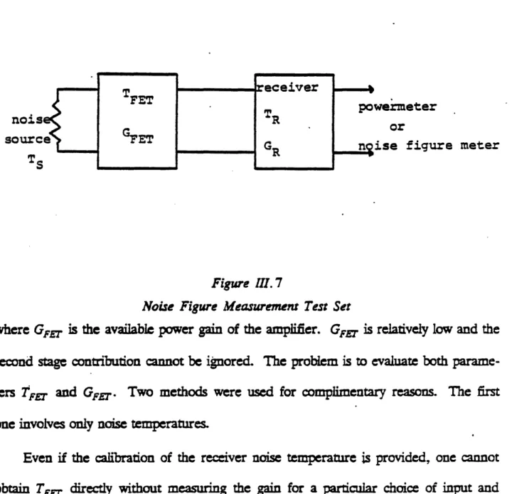
In order to find the intermediate parameters 1l, one has to determine both the noise temperature of the device for a given impedance and the source impedance. Because of the low gain of the experimental amplifier, one cannot measure directly its equivalent noise temperature without introducing a large error. A receiver (necessarily noisy itself) has to be incorporated in the measurement set-up as shown in Figure m.7. The overall noise temperature of the system is given by the Friis' formula
Treceiwr
Toetm TFET + G
GFET
-no.: sourl
T
re meter
Figure 1II. 7
Noise Figure Mesurement Test Set
where GFrT is the available power gain of the amplifier. GFT is relatively low and the second stage contribution cannot be ignored. The problem is to evaluate both parame-ters TFEr and GFu. Two methods were used for compimentary reasons. The first
one involves only noise temperatures
Even if the calibration of the receiver noise temperature is provided, one cannot obtain TET directly without measuring the gain for a particular choice of input and output impedances. The operation is delicate and subject to errors since one has to disconnect the test board from the receiver. On the other hand, if two different receivers are available we have a set of two equations with two unknowns (T.ET, GFET)
that we are thus able to solve. A single reciever that simulated the operation of two different ones was built. This circumvented the problem of having to disconnect and reconnect the amplifier for an additoinal set of measurements. The Figure .8
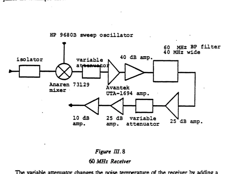
, 0
plifies the technique used.
HP 9680B sweep oscillator
fi Sftez
amp. amp. attenuator
Figure 111. 8
60 MHz Receiver
The variable attenuator changes the noise temperature of the receiver by adding a series resistance to the rcuit, i.e a constant temperature increase. The attenuator was set to achieve 0 or 1 dB attenuation in order to minimi7e the noise temperature of the entire system. In this manner, the measurement errors are minmizd espeially at low gain levels of the FET. The noise temperature of the receiver was found to vary slightly with time, thus causing calibration problems. However, over a short period of time (2-3 hours) the correlation coefficient between the receiver in position 0 and in position 1 was found to be better than .995. The required measurements were per-formed with a noise figure meter. Details of the procedure and of the associated software are listed in Appendix C2.
__._ LLLIL··--L---I -1111111411_- -··-··IIIL^ --I----I---· It r
The second method used the output power of the receiver for different noise sources. The noise level at the output power of the receiver is a function of four
parameters: TFEJ, GFET, T,... and G . By using a noise diode which provides
two levels of noise and by calibrating the receiver, one obtains a system of four equa-tions. The algebra and the software assoated with this method are presented in
Appendix C.
oscilloscope
A cquisiti .Systm ise i r
Data Acquisition System noise figure miter
-The two methods were used simultanously for verification purposes as shown in Figure I3L9.
At first, it was hoped that the use of microstrip formulae would simulate the source impean of a given configuration. However, such non quan fle parame-ters as the amount of solder on the stub, the length of the pin of a feedthrough capai-tance, or more drastically the choice of bking capatance were causing variations in the noise and the gain of the amplifier. The input half of the experimental amplifier was repcated in order to measue the source imedance of a given configuration (see Figure .10). 1.15" .42" .4" .17* .17"
4
-: m~~~~~~~~~~~~~ .15" .15" _0-j4-1
2.25" .10-.130 Figure 111. 10Case for the Measurement of Source Impedances
This board was also used to investigate losses due to the matching network, to cal-culate the noise induced by these losses and to compute the necessary corrections. The
.... -- l~-~L' -~'. IIL L I4~ - .. I^1I-- ·
complete derivation of these results is presented in Appendix C3.
All the noise tbmperatures were measured using the data acquisition system descnbed in Fire Im.9. The amplifier used was the second prototype discussed in section IV.4.
To minimize the receiver's contibution to the noise temperature of the system and thus reduce the error' in the determination of the FE1 noise temperature, the gain of the ampifier (first stage in the Frii's formula) had to be maximized. At first, this was achieved by optimizing the output network of the amplifier. The load impedance presented to the FET was made close to S22 conjugate. The output network of the amplifier affects only the amplifier's gain and not its noise parameters.
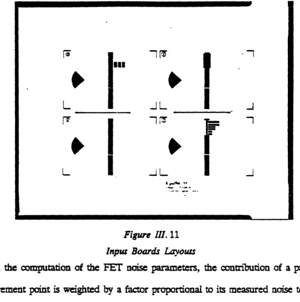
Six different boards were used at room temperature, as input networks to pro-vide the FET with a large variety of source impedances. Each of them could be easily adjusted depending on the particular frequency the noise parameters are measured at. The Figure .11 presents-some of the board's layouts. When cooled, the substrate boards are subjected to mechanical stresses that tend to bind them. To prevent this, the boards are held tightly against the amplifier case with screws and washers. Despite these precautions, two substrate boards could not be used at cryogenic temperatures.
The receiver's noise temperature is fairly high (1000 K) and as a result, when the source impedance is mismatched, the system's noise temperature can be relatively important.
A complete study of the measuement errors is presented in Appendix C2.
III
L JL
.
L~~~~~~~~~~~~. ve _* .*
Figure IIl. 11 Input Boards Layouts
In the computation of the FET noise parameters, the contribution of a particular measurement point is weighted by a factor proportional to its measured noise tempera-ture. Because erors are more important as the noise temperature of the FET incrases, points with a FET noise temperature higher than 800 K were disregarded.
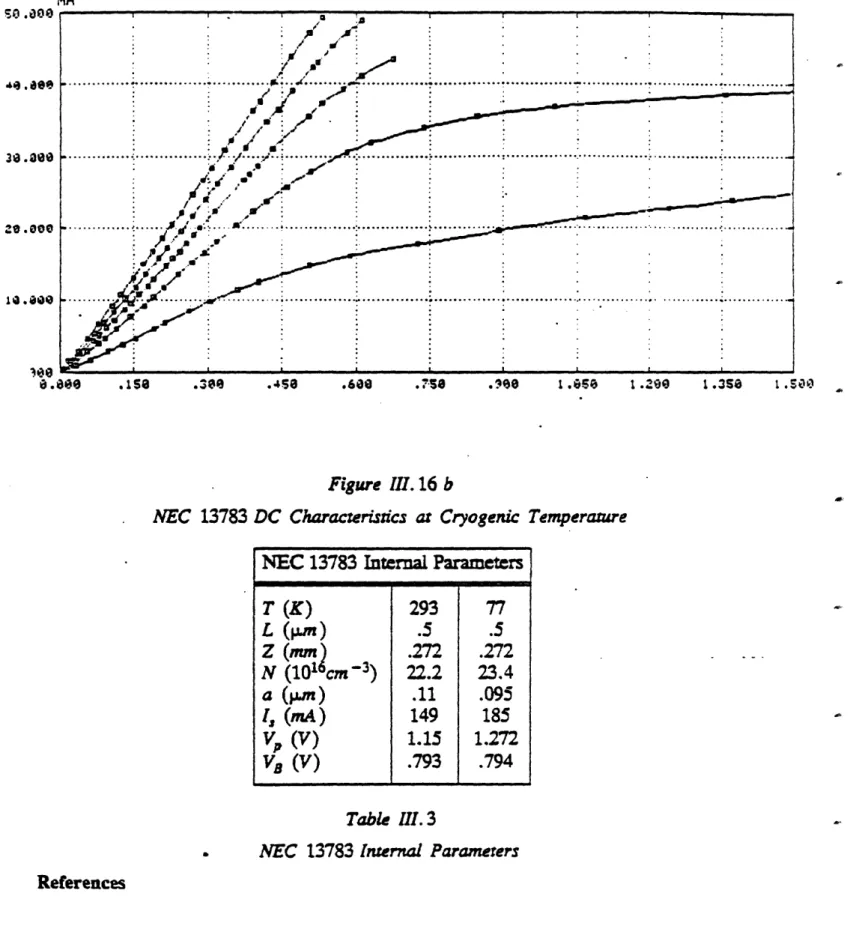
Measurements were perormed for a drain source voltage of 3 V and a drain current of both 10 mA and 30 mA. The FE noise parameters of both room tempera-ture (293 K) and cryogenic temperatempera-ture (77 K) were calculated at 100 MHz intervais between 8.1 and 9.6 GHz. the input board yielding the best results at 8.45 GHz, was subjected to more measurements at other bias to study the latter's dependence on the minimum noise temperature. Tables .2 a and m.2 b present the noise parameters at 8.45 GHz. (All the impedances are referenced to the source edge of the FET
pack-_.__^ ^·-I1-Y-LY- --^IIIII· ·--·--__.XI ·I
age)
Table I. 2 a
NEC 13783 Noise Parameters Id =1 0 mA , Vos 3 V
Table . 2 b
NEC 13783 Noise Parameters 1,d=30 mA, VDS =3 V
Figures 3L 12a and ff.2b present the variations of the .mnmum noise temperature with respect to frequency and temperature. As seen, the cooling to 77 K dramatically improves the performance of the FET.
A power law fit for the noise temperature of the FET of the form
TNO!uE aTe fF
produces the following result: For a bias of 10 mA 3=.80, y1.58 and for a bias of 30 mA 3 =.86 and y=1.66.
Frequency 8.45 GHz
NEC 13783 Bias 10 mA , 3 V Errors
T (K) 293 77 +1 Tmi (K) 126 42 ±7 Rop () 37.2 17.6 -2.5 XOP () 5.0 -.2 +2.5 gn (mmhos) 15.7 7.8 +3.6 Frequency 8.45 GHz
NEC 13783 Bias 30 mA, 3 V Errors
T (K) 293 77 -11 Tmin (K) 150 47 ±7 R, () 45.9 22.3 +2.5 Xo0p (f) -3.3 -. 7 ±2.5 gn (mmhos) 21.0 10.7 +3.6 -~~ ~ ~~~~~~~~~~~~~ I
1 5.i iG .aGG 14.33 9 . GO 1 . 00 I. . .- ... .. ... .. 77 K... ... ... ~~~~~··· · · · .~~·1· · · · · ·. · ... ... ... , , , ,,, ,,, , , ~~~~I ... ...;... . ... ... ...l... . ... ... °. . . . .. . I . ...
:..-
--* -*--
*--*
*. ... ... .... . ... .. ... ....
I.
.3..
.
.
... ... ....
....
... ... .... .. ...
. ..
... ... ... .... . ... ... ... I ; . . -. . . . ! j, ... · ... 8.... . .k. . .'...., . r... . . ... ... .i . . . .t... Figure LI. 12 aNEC 13783 Minimum Noise Temperature Id =10 mA, VDS =3 V
Although the value of the mnimum noise temperature is dependent on the FET DC bias, i variations with frequency and tmptrare are found to be (given the imprcdsions in fhe resllts) independent of the bias. The tempratre dependence of Tm is comparable with published works performed at other frequencies and for other
FEIT's 18,9,10 ]. The theoretical expresson presented in the section I.6 expresses the minimum noise figure as
F=l+b.L+c(~]2
fr fr
The minimum noise temperatre then varies as
As and in the before
fr
is very large +stated to 10 GHz band one appoAs stated before fr is very large and in the 8 to 10 GHz band one can approximate
-trj.q:~ C···.···-··· . . . . .i ... ~s1.s ! s · * , ... . : . ... ;. .r.... .*... ... I . 0 0 .. ... ... .. .... .. ... ... . Lbkd 2 8 i. . .... ... , :. _. 77 K : 30 .voo O -: ... ... ... ... 0 -.J C, t . I I, , , , ' .. ;.. .. ,, -, , .1O !i.Z Figure 1. 12 b
NEC 13783 Minimum Noise Temperature Id =30 mA, VDS =3 V
T by bf/fr. This yields a theoretical factor y equal to 1. The experimental value
of y predicts a higher noise temperature for high frequencies than that of Pucel's
model A fit disregarding measurements performed over 9.2 GHz provides a value y equal to 1.17 for 10 mA (1.16 for 30 mA). That is, with the exception of frequencies
greater than 9.3 GHz ( because of measurement errors), the experiment confirms the
variations of the minimum noise temperature (and therefore of the minimum noise fig-ure) in accordance with Pucl's theory.
The value of the minimum noise temperature T=, was found to be larger that the
value predicted by Sierra [ 11 ] for the NEC 13783'. From the 15 GHz chip noise
Comparison of high frequency noise parameters has to be pformed carefully. This is tue since the mount and surrounding of the transisor= affects the noise temperature of the device by reacave feedback.
parameters measurements, Sierra computed the noise parameters at various frequencies assuming the frequency variation of the Pucel et al. theory. At 8.45 GHz, he predicts a noise temprature Tm of about 110 K. The measurements provide Tas equal 126 K (14% igher). The other calculatons performed by Sierra are for a physical
tem-perature of 15 K. No meas ments at this terature were performed in this study.
The Figures I 13a and b present the variations of the optimum noise impedance at room temperature and at 77 K for bias of 10 mA and 30 mA. In both cases the real part of the optimal noise impedance deceases notably when the amplifier is cooled. From these plots one can conclude that if the input network of an amplifier realizes the optimum noise temperature impedance at room tmperature, it will not achieve it once the amplifier is cooled. The uning at cryogenic temperature will require a lowest real part for the source impl ce, meaning the use of lower impedance transmission lines than at room temperatre. The optimum noise ipedanc depends on the bias of the FET but its variations in the reflexon plane remain small as the drain current varies from 10 to 30 mA.
The variations of the noise conductance gn with frequency and temperature are shown in Figure MI.14a for a DC bias of 10 mA and II.14b for a bias of 30 mA.
The measuremens at room temperature are particularty noisy for the lowest drain current bias. As stated before, in order to reduce the number of high noise tempera-ture measurement points, several input boards had to be used to cover the whole 8.1-9.6 -GHz band. This results in discontinuities for the computed noise parameters.
Among these, the noise conductance gn is the most sensible to measurement errors.
£ACTtNCE COMPONENT
RE£CTiNCE COMPONENT
Figure I. 13 a
NEC 13783 Optimum noise Impedance, VD = 3 V, Id = 10 mA
with the 12.5 mrnmhs value predicted by Sierra. A power law fit of the form
gn aTffY
R=E
-EACTANCE COMPONENT
RuG
REACTANCE COMPONENT
Figure 111. 13 b
NEC 13783 Optimum noise Impedance, VDs =3 V, Id = 30 mA
provides the following results: For a bias of 10 mA =.43, y=2.17 and for a bias of 30 mA =.44 and y =2.26. As for the minimum noise temperature, the variatons of gn do not depend on the value of the DC bias of the FET. Theoretically, gn increases as
MMHO .. r I . . . . .. - . .. ... ... ... ... ... ... ... .. . . . 293 K k __ ; - i'~'77 K .. ... .-.. . . . ,
I
, I . ; . . ;-- - ~~~~~~~~~~~~~~~~~~~~~~~~~~~~~~~~~~~~~~~~~~~~~~~~~~~~~~~~~~6*~~~~~~~~~~~~~~~~~~~~~~~~~~~~~~~~~~~~~~~~~~~~~~~~~~~~~~~~~~~~~~~~~~~~~~~~~~~~~~~~~~~~~~~~~~~~~~~~~~~~~~~~~~~~~~~~_ - _-.3 ,,' $. -- ::,..,,.,Figure . 1.,, . . .1 :6 .? Fig e III. 14 aNEC 13783 Noise Conductance, VD =3 V, Id = 10 mA
the square of the operating frequency. Given the measurement imprecisions, the experiment confirms the theory of Pucel et als'. Between 77 and 293 K the experi-mental temperature dependence of gn is comparable to that found in previous work [10
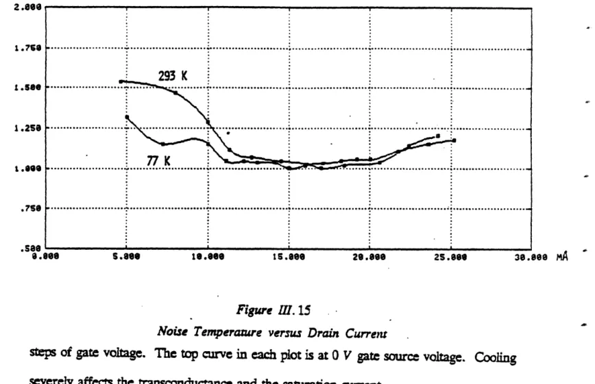
A more complete investigation of the dependence of T, on the DC bias is presented in Figure II15. The variations of the minimum noise temperature versus the drain current are plotted for both room and cryogenic temperatre. In terms of mrimiing Tmin, there is an optimal current whose value depends on the physical tem-perature: 15 mA at 77 K, 17 mA at 300 K.
In conclusion, one can state that the measured noise parameters confirm all the features of the Pucel's theory. A more complete study of the temperature dependence
_.. . M b .. ! 6 .Oe .a ? .000. 4. 0B00 I .,h --c ~ ~ ~ ~ ~ ~ ~ ~ ~ ~ ~ ~ ~ ~ ~ ~ ~ ~ ~ ~ ~ ~ ~~~~~... I