Education and Practice Factory:
Design to First Product Delivery
by
Mingxiu Sun
B.S., University of Illinois, Urbana-Champaign (2014)
Submitted to the Department of Mechanical Engineering
in partial fulfillment of the requirements for the degree of
Master of Science in Mechanical Engineering
at the
MASSACHUSETTS INSTITUTE OF TECHNOLOGY
June 2018
@
Massachusetts Institute of Technology 2018. All rights reserved.
Signature redacted
A u th o r . . . . .. . .. ...
. ...
.... . .. .. . ...
. . . .. . .. .. . . . .. .. . . . .. . .. .. . .. .
Departnent of Mechanical Engineering
Signature redacted
May
25, 2018
Certified by ..
...
Brian W. Anthony
Principal Research Scientist
Thesis Supervisor
Signature redacted
Accepted by...
Rohan Abeyaratne
Chairman, Department Committee on Graduate Theses
MASSACHUSETTS INSTITUTE OF TECHNOLOGY
JUN 2
5
2018
LIBRARIES
Education and Practice Factory: From Factory Design to
First Product Delivery
by
Mingxiu Sun
Submitted to the Department of Mechanical Engineering on May 25, 2018, in partial fulfillment of the
requirements for the degree of
Master of Science in Mechanical Engineering
Abstract
The MIT Education and Practice Factory was launched with support from the Mas-sachusetts Manufacturing Innovation Initiative as part of the education and work-force development program of American Institute of Manufacturing Photonics. It is an advanced manufacturing facility integrated in an academic environment, and is designed to be utilized by three different groups, including researchers, students, and professional manufacturing staff from industry. The current capability of the MIT Education and Practice Factory offers equipment and process solutions for packag-ing photonics products, includpackag-ing chip packagpackag-ing and testpackag-ing. These capabilities fit very well with the research and commerial needs of research groups and industrial partners. The manufacturing scale-up requirements associated with technologies for Test, Assembly and Packaging (TAP) are significant for the photonics industry, and contribute to about seventy percent of the entire production cost. Advances in man-ufacturing technologies are critical to the value-add supply chain. In this thesis, the creation process of the MIT Education and Practice Factory will be reviewed. Three major stages of the project will be covered in detail, including (1) factory setup, (2) pilot products development, and (3) production ramp up.
Thesis Supervisor: Brian W. Anthony Title: Principal Research Scientist
Acknowledgments
First of all, I would like to thank my advisor Dr. Brian Anthony for the great opportunity to work on the Education and Practice Factory. Thank you for the trust to have me taking the lead on such a high-profile project. I have explored and learned a tremendous amount during the last two years. What's more important is that, through this project, I have discovered my passions, in areas such as manufacturing design, product development, process control, quality control, as well as operation and supply chain of a factory. I am amazed and humbled by what we've learned as a team.
I would like to thank AIM Photonics for funding the project, and the trust and
support throughout the year. I would like to thank Dr. Anuradha Agarwal for your extensive guidance on a weekly basis. You are always available for me whenever I need support, especially towards the later half of the project. Thank you Prof. Lionel Kimerling.
There are three major stages of this project, including factory design, pilot product development and production ramp up. I have received help from different groups at different stages on the project.
The factory design stage couldn't be completed without the help from Dr. Xian Du and Dr. Dick Otte. Thank you for your selfless service and insightful advices.
I would also like to thank all the vendors including MRSI, West Bond, Nordson,
Mitutoyo, PXI, ATV, Thermo Scientific and Thorlab. A special thanks to Dr. Yi, Jack, Julius and Peter at MRSI. You have stepped above and beyond to support the customers. We wouldn't be able to produce all those products without your team. Thank you Ms. Samantha Young for helping me with all the logistics work on this project. Thank you to all my lab mates for the help on setting up the factory. This project could not be done without such an amazing group.
The pilot product development stage couldn't be completed without the help from Prof Wei Guo (UMass Lowel) and his student Mr. Ruizhe Yao. Thank you. I would also like to thank Kevin, the undergraduate researcher who has contributed
significantly to this project. Thank you to our laser supplier Mr. Lee from Zenith Optronics for your willingness to selling me the parts despite the small ordering size. Thank you MIT Lincoln Lab for great advices.
The ramp up stage couldn't be completed without the work from Julius, another undergraduate students who is extremely responsive and reliable. Thank you Peter, Jorg, Amir, Kramnik and Jaewhan for helping me develop the quality evaluation plan.
Last but not least, I would like to thank my family. Thank you to my father Yun and my mother Jian for encouraging and supporting me to pursue the Master's Degree at the Massachusetts Institute of Technology. I would like to thank my grandparents Chunniu, Bingrong and Guilan for your love and caring to the family. A special thank you to my grandmother, Juzhen, for being a role model in our lives. You are missed each and every day.
Contents
1 Introduction to the MIT Education and Practice Factory
1.1 Background and Motivation . . . . 1.2 Factory Process Capability . . . .
1.3 How Does the MIT Education Factory Benefit to the Community? . 1.4 Goals of the Project . . . . 1.5 The Operating Team at the Factory . . . .
2 Factory Design
2.1 Introduction to Semiconductor Packaging Industry 2.2 Introduction to the Equipment . . . .
2.3 MIT Education Factory Process Line Design . . . .
2.4 Factory Floor Plan Design . . . .
2.5 Facility Requirement Implementation . . . .
2.6 Equipment Installation Timeline . . . .
2.7 Conclusions . . . .
3 Product Design and Process Development
3.1 Product Concepts Generation . . . . 3.2 Product Design . . . .
3.3 Supply Chain Evaluation . . . . 3.4 Process Development . . . . 3.4.1 Reflow Oven . . . . 3.4.2 Wire Bonding . . . . 23 23 24 26 28 28 31 . . . . 31 . . . . 35 . . . . 45 . . . . 47 . . . . 48 . . . . 52 . . . . 55 57 . . . . 57 . . . . 59 . . . . 63 . . . . 67 . . . . 68 . . . . 71
3.5
3.6 3.7
3.4.3 Die Bonding . . . . Identity three optimized processing methods . . . . Alternative processing approaches . . . . C onclusion . . . .
4 Quality Plan Development and Product Development
4.1 Probe Testing Station Setup . . . . 4.2 Quality Plan Development . . . . 4.2.1 Typical Performance Charts . . . . 4.2.2 Challenges during Probe Testing . . . .
4.3 Product Development . . . . 4.3.1 Product Performance Charts . . . . 4.3.2 Laser-on-Submount Products . . . . 4.3.3 Wire-Bonded Products . . . . 4.3.4 Big Laser-on-Submount Products . . . . 4.3.5 Process Improvement Using Big Die . . . . 4.4 Conclusions . . . .
5 Production Ramp Up, Manufacturing and 5.1 Products selected for Mass-Production . . . 5.2 Production Ramp Up . . . .
5.3 Cycle Time Study . . . . 5.4 Die Bonding Quality Evaluation . . . .
5.5 Mass 5.5.1 5.5.2 5.5.3 5.5.4 5.5.5 5.5.6 5.5.7 )peration Stu
Produced Products Performance Data . . . . Mass-Produced Products Performance Evaluation Small-Die 2-Wirebonded-on-Submount Products . Small-Die 4-Wirebonded-on-Submount Products . Small-Die-on-Heatsink Products . . . . Small-Die Products Overlay Charts . . . . Small-Die Products Burnout Threshold Evaluation Big-Die Products Performance Data . . . .
dy 125 . . . . 125 . . . . 126 . . . . 127 . . . . 129 . . . . 134 . . . . 134 . . . . 135 . . . . 138 . . . . 139 . . . . 140 . . . . 140 . . . . 141 75 80 81 84 87 87 96 98 101 102 102 106 106 114 114 124
5.6 5.7
5.5.8 Big-Die Products Overlay Charts . . . .
5.5.9 Big-Die Non-Lasing Threshold Evaluation . . . .
Operation Study - Operation and Buffer Design . . . . . Conclusion of the Operation Study . . . .
6 Education and Trainings
6.1 MIT Education Factory Activities . . . .
6.2 Education Training Programs with Community Colleges . .
6.3 MIT Education Factory Partnering with Companies . . . . . 6.4 Process Engineering and Manufacture Engineering Training .
6.5 MIT Education Factory Operating Team Training . . . .
6.6 Conclusions . . . .
7 Future Work
7.1 Future Plan in Workforce Development . . . .
7.2 Future Plan for Factory Improvement . . . .
7.3 Future Plan for Process Line Improvement . . . . 7.4 Future Plan for Process Control . . . .
7.5 Future Plan for Education Products . . . .
. . . 144 . . . 145 . . . 147 . . . 154 155 . . . 155 . . . 157 . . . 158 . . . 160 . . . 165 . . . 166 167 . . . . . 167 . . . . . 168 . . . . . 168 . . . . . 170 . . . . . 170
List of Figures
1-1 Chart based on data from a study of Erica R. H. Fochs in IEEE JLT,
vol. 24, No.8, 2006. . . . . 25
1-2 Goals of the Education Factory. There are three major stages of this project, including setting up the factory, developing pilot products and ramping up the production. In each stage, there are well-defined goals to be achieved. . . . . 27
2-1 Semiconductor packaging process flow (Post nano-fabrication, before die test). The processes in the figure labeled with stars are available at MIT Education and Practice Factory. . . . . 32
2-2 Nordson plasma cleaner . . . . 36
2-3 M RSI die bonder . . . . 38
2-4 Eutectic station on the MRSI die bonder . . . . 39
2-5 ATV vacuum reflow oven . . . . 39
2-6 A typical thermal cycle for solder reflow. It includes three major stages, preheat, reflow and cooling. . . . . 40
2-7 West Bond wire bonder . . . . 41
2-8 M itutoyo microscope . . . . 43
2-9 Parts sitting on the microscope work station under inspection. .... 44
2-10 PXI X-ray machine . . . . 46
2-11 Production process flow in the MIT Education Factory. . . . . 47 2-12 All existing equipment have been removed on the factory floor and the
2-13 All existing equipment have been removed and the optical table is kept
in the room. It will serve as a buffer station in the new factory. . . . 50 2-14 Initial floor plan with heavy machines sitting in the middle of the
factory. Big clearances are left around those equipment for engineers to m ove around. . . . . 51 2-15 The final iteration of the factory floor plan. There are three sub-areas
can be found in the factory, including material preparation, assembly and metrology. The figure also shows the manufacturing process flow. 51 2-16 Facility requirement sheet . . . . 53 2-17 Timeline on equipment installation at MIT Education Factory. It's
critical to list information from different vendors on one sheet, in order to keep the installation process well organized. . . . . 54
3-1 Sample product. Laser die soldered on a submount. In this product,
a laser die will be placed on a submount piece. The submount piece is used for even heat dissipation [21]. This product can be readily integrated into other products, such as optical sensors and biomedical d evices. . . . . 60 3-2 Design of the laser-on-submount product integrated into an
experimen-tal setup. The input of this setup will be electricity and the output will be light. With current source attached, electricity will be supplied. With the IR camera attached, the output light can be detected. . . . 61 3-3 This setup is very similar to the setup in the previous figure. In this
case, the IR camera is replaced by a power meter. With the power meter attached, the output light can be measured quantitatively. . . . 62
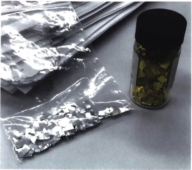
3-4 Small laser dies supplied from Zenith Optronics, they were cut off from a w afer. . . . . 64
3-5 A zoomed out picture of the small laser die. In the picture here are
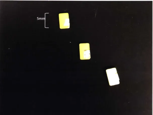
3-6 Laser die supplied from Zenith Optronics. The arrow indicates where the light com es out. . . . . 66 3-7 Specification sheet for the small laser die from the supplier . . . . 66 3-8 300 pieces of Aluminum Nitrite submounts supplied by Prof. Wei Guo,
along with Tin Indium solder pieces. . . . . 67 3-9 Thermal cycle is on going inside the reflow oven. . . . . 69 3-10 Laser-chip-on-solder-on-submount products sitting inside the reflow
oven, ready to be processed. ... ... 70 3-11 Solder piece sitting on submount after reflowing. . . . . 71 3-12 Setting up reflow recipe on the MRSI eutectic station. Temperature
and process time will be setup. More detail please see the MRSI SOP 72 3-13 Practice bonding on a dummy part. Those are 25pm gold wires on
gold surface. . . . . 73
3-14 An example of a good loop shape of a bonding wire. . . . . 74
3-15 This trajectory should be followed when manipulating the bonding
tool, in order to form a good loop. [15] . . . . 74
3-16 MRSI robot head camera sees the small laser dies sitting on a Gel-pack. 76 3-17 Chip on a MRSI vacuum tip . . . . 76 3-18 MRSI sees a laser chip on the image processing screen. . . . . 77 3-19 Optimizing the pattern recognition algorithm on MRSI for a
consis-tent performance. In this case, we are performing an image process technique to blur scratch marks on the bonding pads. . . . . 78 3-20 Process comparison: manual solder versus MRSI solder versus MRSI
epoxy ... ... 80 3-21 Cycle time study (for a batch of 10) at the initial stage of process
developm ent. . . . . 81 3-22 Laser-die-on-solder-on-submount product. The size of the laser die is
250pm *250pm . . . . . 82
3-23 Big laser-die-on-epoxy-on-submount product. The size of the laser die
3-24 Top view pre-soldered submount with Tin Gold layer . . . . 83 3-25 Side view pre-soldered submount with Tin Gold layer. It's a
sand-wiched part with aluminum nitrite in the middle . . . . 84
3-26 Tilted view pre-soldered submount with Tin Gold layer. The part is
3m m *3m m . . . . 84 4-1 The set up of the probe station. It includes a microscope, a probe
station, two probe needles, a current source and a power meter. . . . 88
4-2 It shows a laser-die-on-submount product sitting on the probe station. Above it are two probing needles. . . . . 90
4-3 The probing needle can make ultra-fine adjustments in x, y and z directions by rotating the knobs . . . . . 91
4-4 The current microscope set up has a great magnification range and depth of focus for probing test. . . . . 92
4-5 Here shows the input source and output source. The input source is a Keithey 2400 source meter that is used to bias current. Output instrument is a power meter that measures light intensity. . . . . 93
4-6 Here is a case where the microscope is zoomed out. It allows clear observation on the chip as well as the probing needles. It has a great depth of focus for manipulating needle positions. . . . . 94 4-7 This picture shows a case where the microscope is about 80% zoomed
in. it allows clear observation on the top surface of the chip as well as the probing needles. It has a great depth of focus for landing needles. 95
4-8 after integrating the probing station with a microscope that has an appropriate depth of focus, it makes it a lot easier to collect valuable result, and thus help with evaluation of designs of experiment. . . . . 96
4-9 Typical Laser LI Curve . . . . 97
4-10 IV curve is plotted to estimate the resistance in the laser. It is related to the material of the laser chip. Heat dissipation will not impact the IV curve.. . . . . 99
4-11 Besides the power meter, laser output can also be observed through other methods, including an IR card or an IR camera. That can give a direct visualization of what's happening on the laser chips. The figure shows a Thorlab IR card . . . . . 100
4-12 Light coming out from the edges of the laser chip can be observed. The right side is a lot brighter than the left side, because the right side is the front of the laser chip and that's where the laser shot out from the die. . . . .. . . . . . .. . . . 101
4-13 Laser Specification Sheet . . . . 102 4-14 LI curve for bare die. . . . . 103
4-15 IV curve, the laser resistance with a higher temperature. It happens when the current is increasing. . . . . 104 4-16 Spectrum analyzing result on the laser die. The current is set to be
10, 15, 25, 45, 75mA and the wavelength peaks are 1300nm, 1303nm,
1306nm, 1312nm and 1327nm respectively. Overheating can result shift in peak spectrum . . . . 105
4-17 With the submount on the bottom of the laser die, heat can be dissi-pated evenly on the bottom throughout the entire die. . . . . 107
4-18 PCB design. There is an area for the submount to sit on and that will be connected with the cathode. There are two areas for the wires to bond to and they will be connected with anode. . . . . 108
4-19 PCB substrate from the PCB supplier . . . . 109
4-20 This photo shows a submount device bonded on the PCB and is wire bonded to the bonding pads. 4 wires can be seen in this product. . . 110
4-21 This picture shows the probing process for the submount-on-PCB de-vice. Given that the probing area is more than 100 times bigger than the chip. It's significantly easier to probe than before. The cycle time of testing products was reduced. . . . .111 4-22 LI curve for laser-on-submount-with-2-wirebond. Threshold is at 8mA.
4-23 LI curve for laser-on-submount-with-4-wirebonded. Threshold is at
8mA. Peak power at 55mW and current at 170mA. . . . . 113
4-24 LI curve for laser-on-submount-on-heatsink. Threshold is at 8mA. Peak power at 65mW and current at 180mA. . . . . 114
4-25 Big die under microscope . . . . 115
4-26 Process development of the big die on the MRSI machine. . . . . 116
4-27 Tilted view on the big die glued to a submount. Scratch marks can be observed in row 2 and row 3. The laser does not lasing because of the m
aarks.
. . . . 1174-28 LI curve for big-die-on-submount. Threshold is at 24mA. Peak power at 59.4mW and current at 240mA . . . . . 118
4-29 LI curve for laser-on-submount-with-2-wirebonded. Threshold is at 24mA. Peak power at 70mW and current at 240mA. . . . . 119
4-30 LI curve for laser-on-submount-on-heatsink. Threshold is at 24mA. Peak power at 96mW and current at 360mA. . . . . 120
4-31 It shows the die was bonded with 8 wires to the PCB bonding pad. . 121 4-32 Die was completely burned out with a current input of 1000mA. . . . 123
5-1 It shows the cycle time during the development stage. Now the recipes are set up and optimized, it will take roughly 6 hours to finish a batch of 100 products. . . . . 127
5-2 Ramp up rate in the Education Factory for the last year . . . . 128
5-3 Buffer region in the factory . . . . 129
5-4 The shear test machine. . . . . 130
5-5 This microscopic image shows the pushing head is hitting against the laser die on the submount. Shear test is performing on the laser-on-subm ount product. . . . . 131
5-6 This microscopic image shows the die falls off the submount after the shear test. ... ... . .... .... . . .. .. .. ... 132
5-7 Shear tester shows the force that's needed to push the die off the
sub-mount. 0.124kg is considered a good value for bonding quality. . . . . 133
5-8 This table shows the peak outputs on laser dies are improved with wirebonding and heatsink. . . . . 134
5-9 Average chart of small die 2-wirebonded-on-submount. Lasing thresh-old is at 8mA. Peak power reaches 50mW at 150mA. . . . . 136
5-10 Zoomed-in range chart of small die 2-wirebonded-on-submount. . . . 137
5-11 Average chart of small die 4-wirebonded-on-submount. Lasing thresh-old is at 8 mA. Peak power reaches 60mW at 160mA. . . . . 138
5-12 Zoomed-in range chart of small die 4-wirebonded-submount. Similar trend was observed on this as the previous range chart with 2-wirebonded. 138 5-13 Average chart of small-die-on-heatsink. Lasing threshold is at 8 mA. Peak power reaches 67mW at 170mA. . . . . 139
5-14 Range chart of small-die-on-heatsink. . . . . 139
5-15 Average chart of small die overlay. . . . . 140
5-16 Range chart of small die burnout threshold. . . . . 141
5-17 Average chart of big-die-on-heatsink. Lasing threshold is at 24mA. Peak power reaches 74mW at 280mA. . . . . 142
5-18 Zoomed in range chart of big die 8-wirebonded-on-submount. . . . . . 142
5-19 Average chart of big-die-on-heatsink. Lasing threshold is at 24mA. Peak power reaches 105mW at 360mA. . . . . 143
5-20 Big-die-on-heat-sink products show similar trend on range chart com-pared to 8-wirebonded product . . . . 144
5-21 Big-die LI curve average value sumery chart . . . . 145
5-22 Big-die non-lasing threshold chart . . . . 146
5-23 Process parameter for each equipment in Education Packaging Factory. Once we have all those data, we can start putting numbers into the sim ulation. . . . . 148
5-24 Parameter inputs. p and r values are estimated for all 7 equipment. Buffers are set to be 20 in between each processing step. . . . . 148
5-25 Test 1 results. The production line efficiency is 76.6%. . . . . 149
5-26 Parameter inputs. Buffer sizes are set to be 100 instead of 20 products. 150 5-27 Test 2 results. The line efficiency was improved from 76.6% to 81.6%. 150 5-28 Parameter inputs. Buffer are re-distribution. . . . . 151
5-29 Test 3 results. Production rate was increased with updated buffer distribution. . . . . 152 5-30 Process parameters for each equipment are re-estimated in this chart 153
5-31 Parameter inputs. Probabilities of repair and failure are updated. . . 153
5-32 Test 4 results. A higher production rate is achieved with shorter tool
down time and longer continuous process time. Conclusion from the charts: by hiring a technician to do the monthly maintenance on die bonder, it is possible to further increase the productivity of the pro-duction line. . . . . 154
6-1 American Institute of Manufacturing Summer Academy. Four lab ses-sions are hosted at the MIT Education Factory during the workshop. 157
6-2 A group of students from STCC visiting MIT Education Factory. . . 158 6-3 Working with MIT movie crew to make promotion movie for MIT
Education Factory. . . . . 159
6-4 A sensor product being packaged in the factory. . . . . 161 6-5 A nano-fluidic product is packaged in the MIT Education Factory.
Jaehwan, a designer from the Electrical Engineering Department at MIT, designed a nano-fluidic chip device. In the design, he will need to bond two points with large distance. I was able to sit with him and work on his device and provided with some design devices for a better overall package product. . . . . 162
6-6 A sensing product is packaged in the MIT Education Factory.
Kram-nik, a designer from Electrical Engineering Department at MIT, de-signed a photonics device. In his design, there are bonding pads with tiny pitches. I sat together with Kramnik and work on the design. We gave him some suggestions on the way he could arrange the bonding pads without sacrificing the small size of the footprint. . . . . 163 6-7 256 wires are bonded on the sensing product. Jorg is a research scientist
at MIT. He came up with a design required 256 bonds. The devices are neural probes, which are used to record the activity in the brain. The chip-to-PCB wirebonds in the image consist of two columns of
128 sites each, for a total of 256 wirebonds. We were able to finish the
wirebonding for a few of his devices in two days. . . . . 164
List of Tables
Chapter 1
Introduction to the MIT Education
and Practice Factory
1.1
Background and Motivation
The MIT Education and Practice Factory (EPF) was launched with support from the Massachusetts Manufacturing Innovation Initiative (M212) as part of the edu-cation and workforce development program of American Institute of Manufacturing Photonics (AIM Photonics). M212 was initiated by Governor Baker and the state legislature to develop the Manufacturing USA infrastructure within the state [29]. The Education Factory is an advanced manufacturing facility integrated in an aca-demic environment, and is designed to be shared by three different groups, including researchers, students, and professional manufacturing staff from industry. It is also referred as MIT-LEAP (Lab for Education and Prototyping) [2]. It provides access to equipment and training to users from all groups. It also serves as a great resource for education, such as classes in photonics and advanced manufacturing. Hundreds of students from MIT and other local universities have already benefited from the education component of this facility. Lectures on advanced manufacturing and pro-cess control have been hosted in the factory throughout the year. In addition, the MIT Education Factory is created to serve as a model for other such facilities across the Commonwealth of Massachusetts. The purpose is to better facilitate and
accel-erate advanced manufacturing education in the state, with a joint effort between the government, academia and local businesses.
1.2
Factory Process Capability
The current capability of the MIT Education Factory offers equipment and processing solutions for packaging photonics products, including chip packaging and inspection. These capabilities fit very well with the research and commercial needs of research groups and industrial partners. Prior to the creation of the factory, most research groups and SMEs (small and medium sized enterprises) did not have affordable access to small-scale electronics and photonics packaging. They could modify the designs and improve device performance in the cleanroom, but without packaging the device, they were not able to perform field tests for performance in typical use-case environments. When companies have performed packaging, they have had to pay thousands of dollars and have had to wait for a few months before they could get test results. A few iterations in the product design can take a long time to complete. This is one of the challenges that the MIT Education factory has helped to solve. The factory can significantly reduce the cost and time commitment for research groups. Instead of waiting for months, packaging can be done in the MIT Education Factory within days. It has made possible for more product design variations and quicker turn around compared to an OEM-dependent design team.
To understand this thesis, it is critical to be aware of the definition of packaging. In the photonics industry, product packaging has multiple layers of meaning. They include (1) mechanical packaging of components for physical protection, (2) electrical packaging of components to drive the parts, and (3) optical packaging to transmit and detect light signals [5]. Because so many factors have to be considered at once, this is what makes photonics packaging so challenging. The accuracy requirements are typically in the range from sub-millimeter level all the way down to sub-micrometer level depends on the application [14].
3 5 --- -30 25~~~---- --- -- -- -25 0 15 51--- --- --- -- - -- --- -a 0 S
-Packaging Test Assembly Lithography Other frontend Epitaxy
Figure 1-1: Chart based on data from a study of Erica R. H. Fochs in IEEE JLT, vol.
24, No.8, 2006.
Assembly and Packaging (TAP) are significant for the photonics industry, and con-tribute to more than 70% of the entire production cost. This is mostly due to ultra-precision in optical alignment and coupling requirements. Advances in manufacturing technologies are critical to the value-add supply chain in this industry
161.
To scale up photonics products and keep production costs down, innovations in testing and packaging processes are critical [5]. Unfortunately, this has not been actively pursued in the academic world for the last few years due to an extraordinary-high bar to enter the field. The MIT Education Factory enables an academic focus on those topics. We have demonstrated first scale up of packaged product production to quantities in the hundreds. Those activities are relevant to addressing challenges both to photonics industry and, more broadly, to advanced manufacturing.Our tool suppliers and industry collaborators helped to define current challenges in photonics packaging and testing. At the same time, they provided potential solutions
in product development and process optimization. They have made it possible for the Education Factory to achieve its launch goals in the last two years. The first few products were developed and the manufacturing has been demonstrated. The results were integrated into a few advanced lectures and workshops. Collaborations between researchers, students and the industry serve as the backbone for the activities at the factory.
1.3
How Does the MIT Education Factory Benefit
to the Community?
The photonics packaging capability in the facility is a unique asset to the MIT com-munity. Currently, many MIT device groups have outsourced their packaging work to OEMs(Original Equipment Manufacturers). Outsourcing is generally very costly and time consuming. It may take months for a part to return. With the Education Factory, the cost in packaging would drop significantly for the research groups; lead-time can be as short as a few days. This will allow more room in planning and more flexibility in design of experiments.
For students and researchers who study manufacturing and operation, the Edu-cation Factory provides them with easy access to a operating production line. With process and product development happening in the same room, the manufactur-ing/operation students will have a unique opportunity to work side-by- side with product designers. They will be able to understand the system requirements better and provide valuable information on manufacturability of the products. Inclusion of the production data to optimize a design will help engineers to achieve higher quality in their products.
From the researchers' standpoint, it is not common to have opportunities to test new theories in a real factory, nor is it common to have manufacturing professionals working with them during the design process. With the Education Factory being conveniently located in the middle of the MIT, it becomes possible for close
collabo-Factory Product Consumer Serves as a resource to Run the entire process With some volume the community that will flow with a few pilot produced products, we
be shared by products will study
- Academia - Research on cutting - Manufacturing
- Research edge photonics products - Process control
- Industry - Work with industry on - Operation launching new products
Figure 1-2: Goals of the Education Factory. There are three major stages of this project, including setting up the factory, developing pilot products and ramping up the production. In each stage, there are well-defined goals to be achieved.
ration. It not only makes the entire product development more time effective, but also fundamentally helps researchers to come up with better designs for overall product performance. Since the Education Factory was first created, more than 20 researchers have benefited from the collaborations.
Beyond the conventional product development and manufacturing studies, the Education Factory is a facility for introducing concepts in other related fields. That includes factory design, process line development, process control, new product intro-duction, operation and supply chain studies.
In addition, it has and will support activities involved in non-technical fields, including higher education and workforce training. Since the Education Factory was launched, it has hosted ten hour-long lectures on the production floor for more than 200 students, researchers and manufacturing professionals. More than 150 hours of equipment training have been hosted in the Education Factory and 30 individual engineers have been certified. The focus of the lectures and trainings ranged from photonics technology to manufacturing techniques.
1.4
Goals of the Project
At the beginning of the project, a few goals have been set. Within the first year the goals are to: (1) have the factory set-up, (2) qualify the tools and process, (3) design the first pilot products, and (4) run the first pilot products. Within the first two years the goals are to: (1) run a few pilot products to demonstrate the entire process line, (2) run industry-standard photonics product, (3) train engineers on the equipment, (4) scale up production to 100s, (5) run analysis on the production data and (6) work with researchers in developing photonics products.
1.5
The Operating Team at the Factory
There are three major stages of this project, including (1) factory design, (2) pi-lot product development (it includes product development, process development and quality plan development) and (3) production ramp up stage (including mass pro-duction and quality control).
A total of six undergraduate students have been hired on this project throughout
the entire process at different stages. In the pilot product and process development stage, Mr. Kevin Zheng and Mr. Michael Castillo have been working as process engineers and helping with setting up programs on the processing equipment. In the product development stage, Mr. Jadorian Paul, Mr. Alexander Galitsky and Mr. Emmanuel Havugimana have been working as product designers and helping with design idea brainstorming and identifying suppliers. In the production ramping up and performance validation stage, Mr. Julius Hoang has been working as a quality engineer and helping make quality validation plans and designs of experiment.
Besides the undergraduate students, Dr. Xian Du has provided tremendous help on the factory design and facility during the initial set up stage.
Dr. Brian Anthony and Dr. Anuradha Agarwal have been giving the team exten-sive guidance on the project on a weekly basis for the last two years.
Chapter 2
Factory Design
The purpose of setting up the MIT Education and Practice Factory is to connect education and research with industry. It serves as a factory-laboratory to teach advanced manufacturing concepts and research new techniques [11]. It provides SME (Small and Medium Enterprises) technician training and certification, and allows their engagement in equipment and process development. It supports the AIM MPW (Multi-Project Wafer) and TAP (Test, Assembly and Package) hubs. In order to meet all those needs, it's necessary to understand the packaging industry and study the process flow, and implement them into the MIT Education Factory design.
In this chapter, background of the packaging industry will be introduced. The process on how the MIT Education Factory is set up will be covered, starting from factory floor plan and facility requirement to equipment installation and production line set up. In addition, introduction will be given to each individual equipment, both from the equipment engineering perspective and process engineering perspective.
2.1
Introduction to Semiconductor Packaging
Indus-try
In the photonics and IC industry, post-fabrication processes are necessary to prepare the products for assembly into final consumer products [26]. From chip
manufactur-Figure 2-1: Semiconductor packaging process flow (Post nano-fabrication, before die test). The processes in the figure labeled with stars are available at MIT Education and Practice Factory.
ers, what customers usually receive are bare wafers. Wafers cannot be used and be processed without being properly packaged. Post-processing steps have to be done before the wafers turning into useful components and being ready for final
assem-bly [5]. The following section will give a brief introduction to a typical packaging processes flow.
The flowchart shows the sequence of wafers being packaged. Each step will be introduced in the following according to the order of processing,
1. Back grinding is to polish the backside of a wafer in order to achieve a smooth
surface. A flat backside helps for easy handling of the wafer in the future processes [27].
2. Wafer mounting is to mount a piece of wafer onto a tape before they can be sawed.
a die will vary from 200prm to a few millimeters. There are cases that dies can be as big as a few centimeters [25].
4. After the wafer has been diced, the resulting chips will be cleaned in order to remove any scrap from dicing.
5. Chips need to be sorted into carriers such as tapes, Gel-Paks or waffle packs
before being shipped to the next manufacturer.
6. Once the next manufacturer receives the chips, IPA clean will be performed in
order to wash the surface of the chips.
7. Plasma clean is run when there is a need to remove oxidations or other organic
residuals on the chips [131.
8. After the chips are cleaned, microscope inspection needs to be run for
verifica-tion.
9. After that, the chips are ready for actual packaging processes. Die bonding is
to pick up a piece of chip and place it precisely onto a printed circuit board
[3].
A typical precision accuracy required is on tens of micrometer- scale. Inphotonics packaging, the requirement is significantly stricter than that in the
IC industry, the accuracy tolerance can be as low as 0.25 micrometers. The
bonding mechanism between a chip and a PCB is using conductive epoxy or solder. Some die bonder contains epoxy dispenser on the machine, which can have epoxy applied onto the PCB before placing the die all at one place.
10. After bonding with epoxy, a reflow process is needed to cure it. Vacuum reflow
oven is needed in this case. A vacuum environment can reduce the chances for oxidation to form during the heating up stage.
11. Once the epoxy is cured, wirebonding from the chip to the printed circuit board
12. The strength of the bonds can be tested using a bond tester, which applies pulling forces on individual wires. It will record the forces to ripe apart the bonds. Therefore pulling tests are destructive.
13. Microscope can be used to inspect the bonding, including the sizes and locations. If no defects can be observed, it's time to move on and send the chips to die
level functional testing, which will include electrical and optical testing. The above is a typical process for backend packaging. The process can be modified and changed for the needs of the products. For example, X-ray inspection can be added to monitor the quality of the bonds by seeing through the bonding balls that are formed. If a major void can be observed inside the bonding balls, even though those bonding may have passed visual inspection and electrical test, they are not qualified to be distributed into that market. The void inside of bonding balls may grow bigger when the time passes by. This is especially true for the products that will be implemented in industries with low tolerances for defect, such as biomedical and automotive industry. Shearing test is something that can also be useful to test the bonding quality. It is very similar to the pulling test. While the pulling test grab the wires and pull it away from the joint until it breaks, shearing test pushes an individual die away from its bonding joint point, until the die and the joint are disconnected. Other testing equipment those are useful to have included electrical testing tools, such as a probe station. A probe station is somewhere that a packaged chip can be sitting on, and being electrically connected through probing needles. In the case of evaluating a laser diode, a current versus voltage curve can be plotted with a probe station. In addition, if the probing station is connected to a power meter, it will be able to monitor the optical output. With a laser chip, it will output light intensity for example. In a cutting edge integrated photonics packaging factory, active fiber aligners are also essential to the process [4].
2.2
Introduction to the Equipment
This session will introduce you to each individual equipment in MIT factory in the order of the process flow. The brief introductions are from both the equipment and the process perspectives.
The first equipment is Nordson AP600 plasma cleaner. It's utilized to clean the surfaces of silicon chips. The plasma is created by using high frequency voltages (typically kHz to MHz) to ionize the low-pressure gas. In plasma, gas atoms are excited to higher energy states and are also ionized. If the gas used is oxygen or argon, the plasma is an effective, economical, environmentally safe method for critical cleaning. The UV energy is very effective in the breaking of most organic bonds of surface contaminants. This helps to break apart high molecular weight contaminants.
Different materials require different cleaning processes or recipes. Parameters including power, duration and the kind of gas can be selected. During the process, it vacuums the chamber to remove any contaminants that might oxidize the sample during the cleaning process. When the chamber is sufficiently evacuated, the plasma kicks in, different gases produce different colors during the process. For example, argon produces a light purple color and oxygen produces a white color. When the surfaces of the printed circuit board and chips are plasma cleaned, they become hydrophobic. It will help with the next step, die bonding. The adhesion will be improved between the epoxy and the substrate, and thus provides a higher quality of
bond [18].
The next piece of equipment in the MIT factory is MRSI M3 die bonder. It picks up chips, dispenses epoxy on PCB substrates and places the chips down precisely. It is capable of running program in batch processing, and will perform this pick and place process continuously until the waffle pack has been emptied out. The accuracy of the placement is about 3pm. The smallest chips that it can handle consistently on the MIT model are around 250pm by 250pm. The model in the MIT Education Factory is MRSI-M3, that is a highly versatile model and can be converted into different set ups in a short amount of time. It is a great tool for the packaging
MARCH
factory-laboratory. This model has the flexibility to bring a variety of products from the initial prototyping stage all the way to scaling up. Die bonder is one of the tools that is uncommon for engineers to have access to in the industry, and the process is one of the most challenging steps in the photonics packaging industry. MRSI-M3 tool has been utilized in all the products developed in the MIT Education Factory.
A typical process on the MRSI is to manually load the chips and the substrate
into the machine and then set up a program using pattern recognition techniques. The machine dispenses epoxy on the substrate, then picks up a die and places it on the substrate and gently pushes it down. Process setup, process control, and cycle time studies will be reviewed in detail in the later chapters [31].
To ensure a firm bond, epoxy-curing needs to be done on MRSI eutectic station or a vacuum reflow oven. When doing batch process, a reflow oven is preferred. The ATV reflow oven in MIT Education Factory can heat up to 400 C in a vacuum environment. It uses formic acid for anti-oxidation purpose, and nitrogen as carrying gases.
The thermal cycles required for curing will vary based on the kind of epoxy and the products being processed. A typical soldering reflow procedure may include the following stages, ramp to soak, soak, ramp to peak, reflow at peak temperature and cooling. The parameters that can be modified are temperature and time duration. In addition, carrying gases and chemicals used in the curing process can also be selected
[16].
Once the epoxy is cured and the die is attached to the substrate, wirebonding can be done to form the electrical connection. There are three West Bond wire bonders installed in the MIT factory. Two of them are manual bonders, 7730E and 747630E, and one of them is an automatic bonder 353637F. Among the manual bonders, one is a wedge bonder and the other is a ball bonder. A wedge bonder is good at bonding wires with very small footprint. A ball bonder is good at bonding wires when the arrangements of the bonding pads are in irregular shapes and orientations. The automatic bonder is good at bonding wires when there's a huge amount of wires being required. Especially when there is a need for repeatedly bonding hundreds of
RII-M3
Figure 2-3: MRSI die bonder
Figure 2-4: Eutectic station on the MRSI die bonder
(
217'C LIQUIDUS W 45 -75 SECS
0
RAMP LL Wi RAMP PREHEAT/SOAK TO TO 150-C +i- 20-C PEAKSOAK 60 - 120 SECONDS 1Ic5EC COOLING
I -3'C/SEC 2 -4"C/SEC
TIME
Figure 2-6: A typical thermal cycle for solder reflow. It includes three major stages, preheat, reflow and cooling.
wires in an array.
A typical process on the bonder will be the following procedure. After placing the
substrate under the microscope, turn on the hot plate, heating the substrate makes it easier for bonds to form. Carefully manipulate the handle and create a loop in between the bonding pads [151.
Once wirebonding is completed, parts will be visually inspected using the Mitu-toyo QV Active202 automatic microscope. The automatic microscope has a 1' x 1' workstation that can hold parts. The camera can be moved along X, Y and Z-axis similar to a tool head on a CNC machine. The speed of the movement of the camera can be adjusted, so are the lighting.
A typical process on the microscope would be the following procedure [171. Load
the part on the workstation and adjust the camera position, adjust the lighting of the camera and the height so that the part is in focus. When needed, turn on the recipe editor on the computer and write a program for the task. The program allows the machine to find the pattern on the substrate using automatic pattern recognition. It
I
~7
Figure 2-7: West Bond wire bonder
-
i
a-Figure 2-8: Mitutoyo microscope
-- - - -- -- - -. 1
Finally, to make sure that there are no voids or cavities in the circuit board and wire bonds, x-ray images can be taken for the bonds. A PXI x-ray GenX-90 machine is installed in Education Factory. It is an enclosed unit that prevents any radiation leakage.
A typical process will be loading the parts into the chamber of the x-ray machine.
Turn on the x-ray after to make sure the door is shut. Increase the x-ray dose in order to see through the part. Different materials require different levels of energy to penetrate the chip and form images, so adjust the energy dose accordingly [19]. If you choose the automatic x-ray inspection program, the machine will take measurements and record images automatically. Unlike the die bonder and microscope introduced earlier, this X-ray machine does not use pattern recognition techniques for localiza-tion. It simply uses x, y and z coordinates, which would require the operator to place the part at exact locations precisely each time.
2.3
MIT Education Factory Process Line Design
Among all the processes in the packaging flow chart, the equipment in the MIT Edu-cation and Practice Factory are selected according to a few criteria. The capabilities that they provide 1) are critical component of integrated photonics packaging process; 2) can composite an entire line that provides end-to-end solutions for packaging need;
3) are not readily accessible to researchers and engineers outside of the Education
Factory. In addition, all of them have to be able to fit into the physical space in the Education Factory. With all the equipment, installation and service, the cost should not exceed the $1 million budget.
Eight pieces of processing equipment were selected for the Education Factory among the scope of photonics packaging. They are plasma cleaner, die bonder, reflow oven, wire bonder, microscope and X-ray inspection tool. Multiple vendors were contacted for each individual equipment and quotes generated. In addition to those equipment, a probe test station was set up in a near by laboratory that can help with end-of-the-line testing. With those equipment, the factory has the process capability
I
~w
U
-Figure 2-10: PXI X-ray machine
Plasma Buffer Die Buffer Reflow Buffer
Clean
1 *E
bonder
2Oven
3|X-ray inspection Buffer Micro- Buffer Wire
5 scope 4 bonding
Buffer Probe test
6
Figure 2-11: Production process flow in the MIT Education Factory.
to engage in end-to-end packaging activities.
A buffer space for inline inventory WIP (work-in-process) has been set up on a
large optical table. It has enough room to store up to 200 Gel-Paks. With this inventory storage space, it allows the factory to run batch processes and to optimize the overall production line throughputs.
2.4
Factory Floor Plan Design
The design of the floor plan went through a few iterations. In the initial designs, the heavy equipment were designed to be put together towards the middle of the room, while the smaller equipment were designed to be put towards the sides of the room. In this way a large margin would be left around the heavy equipment. However the challenge of this design is that the equipment would not be arranged in the order of the process. It could cause disorganization in the material flow. It could make it harder to move around on the factory floor with multiple employees working at the same time. It could also make it to be less intuitive for the students to understand the design of the factory as well as the design of the process. As a result, a floor plan
that follows the process flow was created.
The factory is currently designed in a way that is the most intuitive according to the process sequences. It allows for streamlined way of material flow and helps to reduce the WIP handling. The factory floor has been broken down into three sub-areas, including material preparation area, processing area and inspection area. An optical table has been used to serve as a centralized buffer area. It is located in one of the corners, so that the buffer zone will not be in the way of operators during the material handling from one equipment to another, while it is still close enough to every other equipment in the factory.
One of the consultants that provide tremendous help with the factory design is Mr. Dick Otte, who owns an integrated circuit packaging factory in the Silicon Valley. He gave great insights on which equipment that are necessary for the packaging process, as well as how those a equipment should be set up inside factory. Touring Mr. Otte's factory and seeing the material handling in person on the production line was a great learning experience, which help us to set up the MIT Education Factory right on the first try. It allowed us to see the long term picture regarding optimizing the process and maximizing the throughput.
In addition to the technical aspects, the training and education purpose of the factory has also been taken into consideration during the factory design. The factory needs to be set up in a way that is friendly to the students and researchers who has minimum previous experience working in a factory.
2.5
Facility Requirement Implementation
Once the floor plan was made, it was necessary to reach out to vendors to collect the facility specification for each individual equipment. The best way to do it is to list all the equipment on one table, and all the facilities requirement on the same table. That way, it would make the job easier to not to miss any requirement by accident. Common facility requirements may include environmental control, physical constraints, electrical requirement, exhaust requirement, compressed air supply, and
Figure 2-12: All existing equipment have been removed on the factory floor and the space has been cleaned up. It's ready for the new equipment to move in.
Figure 2-13: All existing equipment have been removed and the optical table is kept in the room. It will serve as a buffer station in the new factory.
L~
mMt
>U
tft C&.b
tfzrt
Figure 2-14: Initial floor plan with heavy machines sitting in the middle of the factory. Big clearances are left around those equipment for engineers to move around.
Metrology area
Material
preparation
area
Figure 2-15: The final iteration of the factory floor plan. There are three sub-areas can be found in the factory, including material preparation, assembly and metrology. The figure also shows the manufacturing process flow.
other processing gas supply. Once they're organized in one table, it's straightforward to work with the facility department to get all those requirements fulfilled. The floor plan may be modified to accommodate the facility needs.
2.6
Equipment Installation Timeline
Once a quote has been received from a vendor, it's time to review the specification of the equipment as well as negotiate the price. After that, a few steps may happen before a tool can be installed in MIT Education Factory. It may include but not restricted to the following activities, (1) visit a showroom of the vendor, in order to learn about the specification of the equipment. Sample products can also be tested on the equipment to help understand the capabilities and restrictions; (2) give a tour to the vendor at MIT factory in order for them to better understand the factory's needs and the requirements; (3) provide down payment to book an equipment, typically
10% of the equipment cost. After receiving the down payment, the vendors will now
start building the equipment, a typical lead time can be as short as four weeks to as long as six months; (4) once the equipment has been built, MIT engineers will be invited for an equipment check off at the vendors' factory; at this point, another
50% of the equipment cost is expected to be paid; (5) equipment delivery. Some
equipment vendors will deliver equipment at no extra cost. For others, it is necessary hire movers and riggers; (6) once the equipment is in the MIT Education Factory, now it can be taken out of the freight. The process for moving the equipment from MIT loading dock into the MIT factory, and taking the equipment out of the fridge takes about half a day for a small equipment, and entire day for a large piece of equipment; (7) once the equipment is sitting in the factory, it's time to invite vendors to come over to MIT for the equipment installation and provide training. Before they come, it's necessary to confirm again with the vendor on what has been done on the facility requirements. It's good to go over every single detail, because every factory is different. The assumptions that the vendors make for a typical factory may not necessarily work for the MIT factory. Typically this installation process takes about
Manual Manual Automati Vacuum Automati negative
Tool Name Die Wedge Ball Wire c Wire Reflow c Mah 40C Bonder Wire Bne Bodr Cleaner Ovn Microsco Machine Freezer
Bonderonder Bpe Temp % 10
Clean 10,000 10,000 10,000 10,000 Enviromental Class recomme recomme recomme recomme
nded nded nded nded Vibration Damping ads Height 80 18 18 60 24 24 60 72 80 (in) __________________ Clear 10 12 12 12 12 12 12 12 12 Width (in) 70 36 36 48 24 24 24 48 36 Physical Clear Constraints (in) 20 6 6 12 12 12 12 12 12 Depth 80 36 36 36 48 36 36 60 36 (in) __________ Clear 20 6 6 12 24 24 12 24 12 Weight 7000 50 50 70 50 50 50 200 200 ___________ (Ibs) Voltage/P 208VAC 110V 110V 110V 220V 110V 110V 110V 110V Electrical hase
Amps 20A 10A 14A
Type:Aro
Acid, Argon Formic
Exhaust Heat, O n acid,
Solvent, NOxygen, Nitrogen
other Nitrogen Compressed PSI 80 so 50 50 50 100 air Nitrogen PSI 15 25 60 Oxygen PSI 15 Argon PSI is
forming gas PSI 20
Start date End date Event Location Activity
2016.10.31 2016.11.2 Consulting with Dick MIT Making plans for the factory and products
2016.11.4 2016.11.4 PXI engineer visit MIT PXI engineer visit the MIT factory 2016.11.21 2016.11.21 Mitutoyo tool installation MIT Mitutoyo microscope tool installation
2016.12.7 2016.12.9 PXI tool installation MIT PXI tool installation and installation training
2016.12.14 2016.12.17 West Bond equipment checkoff California Checkoff West Bond in their California factory 2016.12.19 2016.12.20 MRSI equipment checkoff Billerica, MA Checkoff MRSI in their Billerica factory
2016.12.23 2016.12.23 MRSI equipment delivery MIT MRSI equipment delivery to MIT
2017.1.3 2017.1.7 MRSI equipment installation MIT MRSI equipment installation and installation training
2017.1.9 2017.1.9 West Bond equipment delivery MIT West Bond equipment delivery
2017.1.10 2017.1.13 West Bond equipment installation MIT West Bond equipment installation and installation training
2017.1.16 2017.1.19 Factory visit at Dick's factory California Learning from Dick's factory and making plans for the MIT factory
2017.1.30 2017.1.31 Mitutoyo Factory visit Marlborough, MA Visit Mitutoyo Marlborough showroom and training
2017.2.1 2017.2.3 ATV equipment installation MIT ATV oven equipment installation and installation training
2017.2.16 2017.2.17 Nordson equipment installation MIT Nordson Plasma equipment installation and installation training
Figure 2-17: Timeline on equipment installation at MIT Education Factory. It's critical to list information from different vendors on one sheet, in order to keep the installation process well organized.
one week for each equipment; (8) once the equipment has been installed and running properly in the MIT factory. The rest of the bill is expected to be paid. It has now completed the installation process.