Dynamic Nanometer Alignment for
Nanofabrication and Metrology
by
Euclid E. Moon
Submitted to the Department of Electrical Engineering and Computer Science in partial fulfillment of the requirements
for the degree of
Master of Science in Electrical Engineering and Computer Science at the
MASSACHUSETTS INSTITUTE OF TECHNOLOGY
September, 1998
(QMassachusetts Institute of Technology, 1998.
All rights reserved.
Signature of Author ...::: Certified by ..
!
Department of EECS Sept. 8, 1998 Henry I. Smith { Keithly Professor of Electrical Engineering~ J ]:gesis Supervisor
Accepted
by .. - ~~ " .
MASS lIS INSTITUTE Arthur Smith
OF TECHNOLOGY
I
j
C
ai~::.
n_,Undergraduate Thesis Committee_ NQV 1 6
1998 _
~, ..
LIBRARIESDynamic Nanometer Alignment for
Nanofabrication and Metrology
by Euclid E. Moon
Submitted to the Department of Electrical Engineering and Computer Science on Sept. 8, 1998 in partial
fulfillment of the requirements for the Degree of Master of Science
Abstract
Future generations of IC fabrication depend in part on continued improvements in lithography. To meet the lithographic challenges posed by 25-nm lithography, a novel through-the-mask, interferometric imaging alignment method is described that has demonstrated detectivity below 1 nm. A proximity x-ray alignment and exposure system was constructed which incorporates this "Interferometric Broadband Imaging" (IBBI) alignment scheme. 18BI employs complementary grating and checkerboard-type alignment marks on mask and wafer, respectively. Interference fringes are imaged onto a CCD camera when viewing the marks at a Littrow angle of 15 degrees. Alignment is signified by the spatial phase discontinuities between two identical sets of interference fringes that move in opposite directions as the mask is translated relative to the wafer.
The robustness of IBBI was verified by demonstrating that the relative spatial phase is not affected when overlayers of resist, polysilicon, or aluminum cover the alignment marks. Further verification of robustness was found when the illuminating and viewing beams traversed long optical paths through air, glass, and helium. It is significant that JBBJmeasurements are made external to a helium enclosure through the above optical paths, since this allows continuous observation of alignment during exposure.
Feedback stabilization was developed to nullify the effects of thermal drift and mechanical disturbances during exposure. Over several hours the relative position of the mask and wafer was demonstrated to be locked to within 0'=1.4 nm.
Thesis Supervisor: Professor Henry I. Smith Title: Keithly Professor of Electrical Engineering
Dedication
To the letters P, 0, A, L, A, T, M
and the numbers 2, 6, 21, 250.
Quoteable Quotes:
tt...th'ere 5Qpar y In my mln ...t' . d " - Alberto Moel
Acknowledgements
A great debt is owed to Prof. Hank Smith for his faith in me and his receptivity to ideas, to say nothing of his incisive questions that always go right to the heart of the matter, his inspirational presentation style and his superhuman enthusiasm.
Many thanks are due to David Breslau, whose talent in design was always a source of inspiration and pleasure.
To the students and staff in the NSL who made the lab an enjoyable place to work:
First, I would like to thank Alberto Moel, who mentored me through my first years as a UROP. His unique, vibrant, and sometimes unpredictable personality was one of the best parts of working in the lab. I will never forget his rendition of opera songs in the cleanroom at 3 in the morning.
To Jawoong Lee, who gave me the sense of having been to South Korea, and who was forever leaving me with insights into the differences, as well as the similarities between our countries.
To Patrick Everett, who constantly reminded me of the meaning of a good experiment.
To Maya Farhod, who often injected energy and brightness into some otherwise dull days.
To Mark Mondol, for his memorable Christmas parties, and for introducing me to tofu dogs.
To Kathy Early, who showed us that an 8kY voltage is not always lethal. To my parents, for their love.
Finally, a debt is owed to RUSH for the following song, capturing a defiant (poetic) energy that sometimes helps one to push on through the most challenging periods:
Cut To The Chase It is the fire that Ughts itself But it burns with a restless flame
The arrow on a moving target The archer must be sure of his aim
It is the engine that drives itself But it chooses the uphUl climb
A bearing onmagnetic north Growing farther away all the time
Can't stop -- moving Can't stop -- moving
Can't stop YOU MA Y BE RIGHT ITS ALL A WASTEOF TIME I GUESSTHATS JUST A CHANCE
I'M PREPAREDTO TAKE A DANGERI'M PREPAREDTO FACE
CUT TO THE CHASE It is the rocket that ignites itself And launches its way to the stars
A driver on abusy freeway Racing the obUvious cars It's the motor of the western world
Spinning off to every extreme Pure as a lover's desire EvHas a murderer's dream Young enough not to care too much
About the way things used to be I'm young enough to remember the future
--The past has no claim on me I'm old enough not to care too much
About what you think of me But I'm young enough to remember the future
And the way things ought to be WHAT KIND OF DIFFERENCE
CAN ONE PERSONMAKE? CUT TO THE CHASE
CONTENTS
1) INTRODUCTION
1.1 REMOTE DETECTIVITY AND ROBUSTNESS ANALOGy 12
1.2 ALIGNMENT CONTEXT 14
1.3 OBSTACLES TO NANOMETER ALIGNMENT 18
1.4 THESIS OUTLINE 20
2) INTERFEROMETRIC BROADBAND IMAGING (IBBI) ALIGNMENT
2.1 PAST ALIGNMENT APPROACHES 22
2.2 PRINCIPLES OF INTERFEROMETRIC BROADBAND IMAGING ALIGNMENT .. 27
2.3 DETECTIVITY 32
2.4 CAPTURE RANGE 33
2.5 DESIGN CRITERIA SUMMARY 37
3) IMAGE ANALYSIS
3.1 SPATIAL PHASE DETECTION 40
3.2 NON-INTEGER FRINGES 44
3.3 MASK-WAFER AND CAMERA ANGLE 46
3.4 WIDE ACQUISITION ALIGNMENT 48
3.5 SPEEDAND EFFiCiENCy 50
4) ALIGNMENT AND X-RAY EXPOSURE SYSTEM
4.1 SYSTEMARCHITECTURE 52
4.2 X-RAY SOURCE 56
4.3 NANO-POSITIONING STAGES 60
4.4 HELIUM ENCLOSURE 67
4.5 BROADBAND LIGHT SOURCE 70
4.6 MiCROSCOPES 72
5) EXPERIMENTAL VERIFICATION: IBBI DETECTIVITY AND ROBUSTNESS
5.1 ALIGNMENT DETECTIVITY 75
5.2 DETECTIVITY VARIATION WITH GRATING PERIOD 81
5.3 IMMUNITY TO PROCESSCOATINGS 83
5.4 INSENSITIVITY TO ENVIRONMENTAL CONDITIONS 87
6) MEASUREMENT CORROBORATION WITH TWO MICROSCOPES
6.1 EXPERIMENTAL SETUP 90
6.2 IBBI-TO-IBBI COMPARISON 93
6.3 IBBI-PIEZO COMPARISON 94
6.4 OBSERVATION OF MAGNIFICATION OFFSET 97
7) FEEDBACK-STABILIZED ALIGNMENT
7.1 THERMAL AND MECHANICAL INSTABILITY: DRIFT AND FLUTTER 101
7.2 FEEDBACK STABILIZATION TO ONE NANOMETER 106
8) CONCLUSION AND FUTURE EFFORTS 110
APPENDIX A
OPERATION OF EXPOSURESySTEM 114
APPENDIX B
DETECTION AND CONTROL SOFTWARE 117
APPENDIX C
MICROSCOPEALIGNMENT 134
APPENDIX D
HEAD 4 MECHANICAL DRAWINGS 137
BIBLIOGRAPHy 163
LIST
OF
FIGURES
FIGURE 1-1: ARTIST'S CONCEPTION OF THE INTERNATIONAL SPACE STATION •••••••••••••••••••• 13 FIGURE 1-2: NATIONAL TECHNOLOGY ROADMAP FOR SEMiCONDUCTORS •••••••••••••••••••••••• 16 FIGURE 1- 3: NTRS PREDICTED OVERLAY BUDGET •••••••••••••••••••••••••••••••••••••••••••••• 17 FIGURE 2-1: IBBI ALIGNMENT INFORMATION IS CONTAINED IN THE SPATIAL PHASE ••••••••••••••• 27 FIGURE 2-2: INTERFERENCE FRINGES ARE GENERATED BY SUPERPOSiTION •••••••••••••••••••••••• 28
FIGURE 2-3: SCHEMATIC OF IBBI ALIGNMENT 29
FIGURE 2-5: Two IBBI MARKS ELIMINATE PHASE AMBIGUITY 34
FIGURE 2-6: FINE FRINGE ALIGNMENT, COARSE FRINGE AND BAR MiSALIGNMENT ••••••••••••••••• 36
FIGURE 3 -1: STEPS IN PHASE DETECTION ALGORITHM ••••••••••••••••••••••••••••••••••••••••••• 41
FIGURE 3-4: IMAGES OF THE SAME FRINGE PATTERN WITH THE ROI SHIFTED •••••••••••••••••••• 45
FIGURE 3-7: INTENSITY DISTRIBUTION OF A SLICE THROUGH A BAR-MARK IMAGE ••••••••••••••••• 49
FIGURE 4-1: I BBI ALIGNMENT AND EXPOSURE SySTEM 53
FIGURE 4-2: SCHEMATIC OF ALIGNMENT/EXPOSURE SYSTEM 55
FIGURE 4-3: PHOTOGRAPH OF AN ELECTRON-BOMBARDMENT X-RAY SOURCE 58
FIGURE 4-4: X-RAY SOURCE IN OPERATION 59
FIGURE 4- 5: SCHEMATIC OF MASK AND WAFER 61
FIGURE 4-6: PLOT OF THE MAXIMUM ALLOWABLE MASK-SAMPLE GAP •••••••••••••••••••••••••••• 62
FIGURE 4-7: MIT X-RAY MASK STRUCTURE 64
FIGURE 4-8: PHOTOGRAPH OF MASK AND WAFER WITH WAFER STAGE ••••••••••••••••••••••••••• 65 FIGURE 4-9: PHOTOGRAPH OF MASK IN MASK STAGE •••••••••••••••••••••••••••••••••••••••••••• 66 FIGURE 4-10: ATTENUATION OF (UL X-RAYS THROUGH AIR/HELIUM MIXTURE ••••••••••••••••••• 68
FIGURE 4-12: MULTI-LINE ARGON LASER AND REMOTE CONTROL BOX ••••••••••••••••••••••••••• 71 FIGURE 4-13: UNIPHASE ARGON LASER SPECTRUM •••••••••••••••••••••••••••••••••••••••••••••• 72 FIGURE 4-14: IBBI MiCROSCOPE ••••••••••••••••••••••••••••••••••••••••••••••••••••••••••••••• 73
FIGURE 5-1: FRINGE PATTERN OBSERVED THROUGH I BBI MiCROSCOPE 79
FIGURE 5-3: VARIATION OF ALIGNMENT DETECTIVITYWITH GRATING PERIOD 82
FIGURE 5-4: IMAGE OF AN IBBI ALIGNMENT MARK ETCHED INTO SiLICON •••••••••••••••••••••••• 83
FIGURE 5-5: IMMUNITY OF IBBI TO OVERLAYERS OF RESIST 84
FIGURE 5-6: COMPARISON OF ALIGNMENT UNDER DIFFERENT OPTICAL PATHS •••••••••••••••••••• 87
FIGURE 5-7: EFFECT OF HELIUM FLOW ON IBBIIMAGES 89
FIGURE 6-1: ALIGNMENT OBSERVED AT TWO MARKS SiMULTANEOUSLy 91
FIGURE 6-2: TABLE OF STEPS TAKEN PRIOR TO EXPERIMENTS 92
FIGURE 6-3: Two IBBI MICROSCOPES ALTERNATELY OBSERVE ONE MARK 93
FIGURE 6-4: AGREEMENT BETWEEN TWO SIMULTANEOUS IBBI MEASUREMENTS •••••••••••••••••• 95
FIGURE 6-5: PRINTING MAGNIFICATION DUE TO X-RAY POINT SOURCE ••••••••••••••••••••••••••• 97
FIGURE 6-6: IBBI MEASUREMENTS AT MARKS SEPARATED IN THE X-DIRECTION 98
FIGURE 6-7: IBBI MEASUREMENTS AT MARKS SEPARATED IN THE Y-DIRECTION ••••••••••••••••••• 99 FIGURE 7-1: VIBRATION OF MASK/WAFER DETECTED SiMULTANEOUSLy ••••••••••••••••••••••••• 102
FIGURE 7-2: DRIFT TRENDS OF TWO MICROSCOPES 103
FIGURE 7-3: 150 NM DRIFT IN ALIGNMENT OVER SIX HOURS 104
FIGURE 7-4: RESPONSE OF FEEDBACK SYSTEM TO LARGE MiSALIGNMENTS ••••••••••••••••••••••• 107
FIGURE 7-5: SIX-HOUR ALIGNMENT DATA WITH CLOSED-LOOP OPERATION •••••••••••••••••••••• 109
CHAPTER 1:
INTRODUCTION
1. 1 Remote Detectivity
and Robustness Analogy
Let us set the stage with an analogy. Imagine floating in space (Fig. 1-1) and watching the Earth revolve below you. Naturally, you are interested in the goings-on below you. This is of special interest to you since you are on the team building the International Space Station and you are in desperate need of resupplies from Earth to repair the latest system glitch. Your communications are out, but fortunately, you were an optics guru before becoming an astronaut, and you happened to bring a telescope of your own design with you on this visit to the space station. The first thing on your mind is: have the orders been signed to approve the launch of your replacement parts? Now this special telescope has the remarkable power to detect the position of objects
on the Earth to within a millimeter, even though you are orbiting at an altitude of 200 miles.
Figure 1-1: Artist's conception of the International Space Station.
As you peer down into NASA headquarters, to your relief you see the Chairman of Space Supplies writing a letter. Using some custom motion-tracking software, you trace out the position of his pen as he writes on the form. Clouds drift over NASAas you are tracking his pen, but your device is not disturbed by their intrusion. To make a long story short, the tracking software traces the words "Send supplies IMMEDIATELY" and you receive the vital components by shuttle the next day.
Considering the reputed resolution of spy satellites, the detectivity of the optics in this fanciful story is not that farfetched. (Of course, we are setting aside the fact that the numerical aperture of such a telescope would be far too large to pack with your personal effects). The point is that both high resolution and immunity to spurious influences can be achieved at relatively long distances. The optics employed in this thesis have a detectivity-to-working distance analogous to the telescope in the story. And this has many advantages, as this thesis will demonstrate.
1.2 Alignment Context
Let us consider the problem of alignment in a simple, mundane context. Every time you make a sandwich you are unconsciously doing alignment. You take a slice of bread, apply a thin film of mayonnaise, align and place a slice of cheese, perhaps some lettuce and tomato, and another slice of bread. In each step you are following the basic premise of aligned fabrication. The success of your culinary attempts depends in large measure on your ability to properly align all the layers of different materials. Consider how difficult it would be to eat a sandwich that had the cheese drooping off one side and the tomato sliding out the other side! In a similar way, a transistor should have its component layers aligned to 1/10th of the size of the gate.
In our modern society, so thoroughly integrated with computers, alignment is of considerable commercial and technological interest. To remain competitive, computer chip manufacturers must continuously increase the performance of their products. Historically, decreasing the size of the transistors in the chip has done this. Several advantages accrue with diminishing dimensions:
• reduced power consumption (good for handheld, portable devices) • reduced signal propagation time
• reduced switching delay • increased clock speed
To continue the miniaturizing trend there are two fundamental steps that must be taken. The first is to use a wavelength of light that is small enough to define the features. The second is to align a mask and a wafer to about 1/10th of the minimum feature size.
Presently, semiconductor fabrication plants make chips with 250 nm minimum feature sizes, or design rules. Over the past 20 years, the miniaturization has followed Moore's "Law", steadily halving feature size every year and a half. Recently, even in the face of increasing technological difficulties, the trend has accelerated. The National Technology Roadmap (Fig. 1-2) now predicts feature sizes (single lines) of 100 nm by the year 2003.
First Year ofIeProduction 1994 1997 1999 2001 2003 2006 2009 2012 250 248mlOUV 1&1 248 nm OVV .~ . .S 1:.J 248nm OVV Q) N Ci5
5
ii Q) 130 u.. E :J E .~ ~ 100 70 soCootln''£US ItT1provtJomtJontsInreSiO'1.JtlO.'\. o~'erI8Y. reSIsts masl:'fTl~1oog and metrOlOgy volt.'\ A prCXIC1I'Ae 3ppro~h 10 En~;ronmenl Sa.'Pt)'.and Health
C=:J oU;amIC~II()n"Pro-ProduCllon
Figure 1-2: National Technology Roadmap for Semiconductors (1997).
The choice of lithography for 100 nm linewidths is not yet settled, but of all the contenders, proximity x-ray lithography is the most mature. It is therefore logical to use x-ray lithography as a test vehicle for an alignment system, as described in this thesis. But regardless of the lithography, the
overlay issue must be addressed. Figure 1-3 illustrates the overlay accuracy required in the near future, as specified in the 1997 NTRSroadmap.
Year ofFirs/ Product Ship/llcm
'/I'd /Ill/logy G"lIl.'r;1/ ion
Gale CD colltrol (11m)
FllIillCDoutput IIwtrology precisioll (11111.3 sigma) •
Overlil)' COlli rol(11111)
Overlil)' OUlput IIlctrology pr('clsioll (11m.:lsigma)'
So/lll iOlls Exis/ ~I __ ~
1997 199!J 2UUl ZOO] 250 11111 /8011111 '501111/ I:W 11111 20 14 12 10 4 3 2 2 85 65 55 45 9 7 6 5
So/lll iOlls Bf'illg Pursued I NoKmJ\\n Solwloll
• !\/f'iI.\Urr'1II1'/II/Ool /If'rfonllill'rl' /I('('(1s /()IJI'IlIrlI'Pl'IIr11'rl/ orlilll' sl';I/)I', IIIif' III;/Il'riilb. illlri r11'IISil}' of lillf'.s
Figure 1-3: NTRSpredicted overlay budget (1997).
As we can see, within the next 10 years the overlay control must be at least 25 nm and the 3cr precision must be 3 nm. These are challenging requirements. However, the limits to lithography lie at about 25 nm design rules. It is therefore our goal to invent and implement a robust alignment system that can meet the requirements of all presently foreseeable lithography and provide a metrological tool with sub-nanometer detectivity under a wide range of conditions, in essence, one-nanometer alignment detectivity and placement.
1.3 Obstacles to Nanometer Alignment
If you are still thinking about that example of the sandwich, it may not appear there is much difficulty to alignment. But on the nanometer scale, obstacles to alignment abound. The most obvious problem is that of detection: displacements on this scale cannot be seen using ordinary optical microscopes. The limit of resolution of a microscope is given by
p=_A_
2(NA)
where P is the spatial period, A is the wavelength and NA is the numerical aperture. A high-quality Leitz 100x, 0.8 NA objective can resolve 200 nm features, but this is obviously insufficient for alignment on the order of one nanometer. As is well known, the preferred approach is to use interference of light, allowing an increase of over three orders of magnitude in detectivity over an optical microscope.
But detectivity is only the beginning. As one might imagine, greater sensitivity can imply greater susceptibility to spurious influences. It does no good to have a sensitive alignment scheme if it can be easily corrupted by multitudinous influences. These influences include variations or defects in the alignment marks, thin-film interference effects from translucent coatings on the marks, turbulence in the atmosphere between the marks and the optics,
pointing stability of the illumination and different indices of refraction of gases in the optical path.
Perhaps the most fundamental obstacle is that what appears to be solid and immutable on the macroscopic scale is quite flexible on the nano-scale. Materials flex and bend easily, and generally behave more like rubber than steel. The slightest change in temperature will cause significant expansion or contraction of most materials. For every 0.1 degree C variation in temperature, a 10-cm aluminum stage expands by several tens of nanometers.
A consequence of the flexibility of materials is that the measurement must be made at the position of importance to have much meaning over any period of time. Laser interferometers, for instance, suffer from several of the drawbacks just mentioned: they are currently capable of detectivity below 0.3 nm [1], but are limited by variations in the index-of-refraction of the atmosphere, the flatness of the mirrors, etc. Even if these factors can be taken into account, the fact that the laser interferometers measure the position of the edge of a sample holder means that thermal expansion will introduce disparities between the position of interest on the sample and the position read by the laser interferometer.
The basic message is that position, and therefore alignment, is not a static quality on the nano-scale. Even if objects are positioned with nanometer
accuracy in the first place (which is quite a challenge) they will not remain aligned over time.
1.4 Thesis Outline
The purpose of this thesis is to find a method of detecting the relative position of two objects to better than one nanometer. Equally important, this method should not be susceptible to extraneous influences. Once the metrological problems are addressed, this thesis will describe a method of locking the position of the two objects to within about one nanometer over indefinite periods of time. Chapter 2 will describe the principles of the Interferometric Broadband Imaging alignment scheme. Chapter 3 will respond to the issues of interferometric-fringe spatial-phase analysis. The implementation of IBBI alignment in an in-house, custom-built alignment and exposure system will be described in Chapter 4. Then in Chapter 5 several experiments are related demonstrating the detectivity and robustness of IBBI alignment. Chapter 6 goes on to describe the sub-nanometer consistency found between two microscopes observing the same mark, as well as two different marks during a piezo scan of the mask, and scale consistency found between IBBI and the printing-magnification effect from an x-ray point source. Chapter 7 describes observations of drift and vibration in the alignment system and
makes the case for using feedback to control drift and vibration, even during exposure. With feedback, the alignment stability is shown to be cr= 1.4 nm over six hours. Chapter 8 concludes the thesis and makes suggestions for future improvements.
CHAPTER 2:
INTERFEROMETRIC BROADBAND IMAGING
(IBBI) ALIGNMENT
2. 1 Past Alignment Approaches
Previous alignment schemescan be divided into two broad categories: • optical schemes based on imaging geometric objects in a high-magnification microscope, and
• interferometric schemes based on the interference of light diffracted from gratings or zone plates on the mask and wafer.
Interferometric schemes can be further subdivided into those which detect the amplitude and those which detect the phase of an interferometric signal. In this section we will describe examples of, and delineate the strengths and weaknessesof each scheme.
A variety of universities and companies have pursued improved alignment methods applicable to x-ray lithography. In industry the current participants are SussAdvanced Lithography, Silicon Valley Group Lithography in the United States and Canon, NTT, Sumitomo and Toshiba in Japan. The universities having done work in this field are the University of Wisconsin, Louisiana State University, and MIT. The following examples will focus primarily on what has been done in industry, since that is the real-world application, and therefore represents the most wide-spread use of the respective alignment schemes.
Over the years, optical magnification alignment schemes have been the mainstay of the semiconductor industry. Perhaps the most refined example of a geometric imaging optical alignment scheme applied to x-ray lithography is found at Suss Advanced Lithography, a spin-off company of Karl Suss specializing in x-ray steppers. In the SALaligner, high-magnification, high NA optics image a set of horizontal and vertical bars on the mask, similar to a tic-tac-toe pattern. On the wafer there is a complementary pattern, which creates a set of box patterns when aligned. An image of the box pattern is formed on a CCD camera. The image is analyzed by an edge detection algorithm to determine the spacing between the boxes. Since the basic element of the pattern repeats several times, the spatial period of the pattern can be used for error checking. With this scheme, alignment detection of 3a = 17 nm has been demonstrated [2]. This approach has the advantage of a long
heritage, many worker-hours of development and experience in a widely installed user base, but has the disadvantages of costly optics and on-axis operation. That is, the microscopes must view the marks at normal-incidence at a millimeter or so from the mask. Since the microscopes block the exposure path, they must be moved out of the way prior to exposure, thus forcing an artificial and undesirable separation between the alignment and exposure operations. This impacts integrated circuit (Ie) fabrication in two important ways. First, throughput is compromised by the time taken at every exposure to move the microscopes into and out of the exposure path. In the second way, as device features shrink, the structural stability of the stepper comes into question. Short exposure times achieved with a synchrotron source ameliorate this problem, but the flexibility of materials on the nanometer level demands that greater engineering efforts must be focused on achieving structural stability. The cost/performance curve is not favorable at this level: marked increases in efforts and cost can only achieve minimal gains. One of the arguments developed in this thesis is that a more potent long-term strategy is to pursue closed-loop alignment. This argument is likely to have increasing strength as the transition from global alignment to site-by-site alignment progresses.
An example of interferometric-based alignment is presented by SVGL. This scheme utilizes a linear grating on the mask and a checkerboard grating on the wafer. These marks are illuminated at an angle by a set of lasers of various
wavelengths. The diffracting beams from these gratings are detected at an off-normal angle with a photodetector. By scanning the mask and wafer past each other, a series of amplitude peaks are found. These peaks are contained within an envelope. Alignment is determined by locating the center of this envelope and correlating it with the position of the stage. After the scan, the stage is moved back to the calculated "aligned" position. The published performance data for this method is a 30' of 40 nm [3]. The advantage of the SVGL scheme is that it can work without blocking the exposure path, but there is a potential problem: alignment cannot be detected without scanning the mask or wafer. It seems counterintuitive to require a movement in order to detect a position. It also makes great demands upon the stages, since they must move back to a predetermined position with nanometer accuracy. Of course, the position of the stages can be sensed with laser interferometers, but the interferometers, however good their detectivity, cannot tell us the truly meaningful information - what the alignment condition is at any point of interest between the mask and wafer. Drift and vibration may occur between the mask and wafer regardless of the quality of the interferometrically controlled stage position. In sum, perhaps the fundamental flaw in this scheme is that it is based on detecting the amplitude of an interference signal.
To overcome some of the limitations described above, an alignment scheme called On-Axis Interferometric (OAI) alignment based on a comparison of the spatial phase of two periodic patterns was developed in the 1993 MIT
Ph.D. thesis of Alberto Moel. A grating of period P1 on a mask was superposed upon a grating of similar period P2 on a wafer. A CCDcamera with a 20x Leitz objective imaged interference fringes under white-light illumination. To determine alignment, the spatial phase of these interference fringes was compared with a fiducial grating of the same period as the fringes, etched into the wafer. Although 30' = 18 nm alignment in exposed features was
demonstrated [4], this scheme suffered from several disadvantages. First, as in the SALaligner, the microscope was positioned normal to the mask, precluding the possibility of observing alignment during exposure. Second, the fringe contrast was very low due to specular reflections from the mask and wafer. Third, the fiducial grating on the wafer was subject to distortions caused by overlayers. The overlayers, such as photoresist or aluminum, would change the spatial phase of the two patterns in different ways, resulting in spurious alignment signals.
The alignment scheme described in this thesis finds its roots in GAl alignment, but Interferometric Broadband Imaging (IBBI) alignment includes numerous improvements and additions that enhance its potential for future industrial applications.
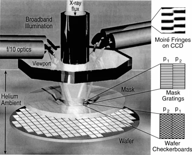
2.2 Principles of Interferometric Broadband Imaging
Alignment
To address the present and future alignment needs of lithography, in particular, proximity x-ray lithography, a novel through-the-mask, site-by-site alignment scheme was invented at the MIT NanoStructures Laboratory. This scheme, termed Interferometric Broadband Imaging (IBBI) alignment, achieves interferometric sensitivity through a comparison of the spatial phase of two periodic interference patterns. Alignment is encoded in the spatial phase discontinuity across the fringes. Figure 2-1 shows several images of fringe patterns with a sequence of spatial phase disparities.
(a) (b) (c) (d)
....
----
--.-...
---(e)
Figure 2-1: IBBI alignment information is contained in the spatial phase of a pair of
interference patterns. Images (a)-(e) illustrate spatial phase disparities corresponding
to steps of 50 nm.
These interference fringes are created by diffraction of spatially-coherent broadband illumination from complementary gratings on a mask and wafer. The period of the fringes, P, is related to the grating periods P1 and P2
by
The grating arrangement requires gratings with periods P1 and P2 side by side on both mask and wafer, but with period P1 on the wafer facing period P2 on the mask (Fig. 2-2), and period P2 on the wafer facing period P1 on the mask. In this manner, matched sets of interference fringes are created which move in opposite directions. The counter-motion of the fringe sets further increases (doubles) sensitivity.
t
+
J Mask: Gratings Ph Wafer: Checkerboard Gratings Interference Fringes on CCOFigure 2-2: Interference fringes are generated by superposition of gratings and
checkerboard patterns on the mask and wafer, respectively.
Displacement is magnified in the spatial phase of the interference patterns. Each interference fringe set magnifies the relative displacement of the mask and wafer by the factor M, where
M_1 p,+pz
- 21p, - Pzl'
The fringes are imaged by low-NA optics onto a CCD camera (Fig. 2-3). The microscopes operate at a large working distance (110 mm) and are employed for both illumination and imaging (as described in Chapter 4).
Interferometric magnification of displacement allows the use of low-NA microscopes to observe nanometer displacements at a working distance of more than 10 cm, in marked contrast to the working distance of a few millimeters required by high magnification optical microscopes.
Mask Gratings
P2
P
1Wafer Checkerboards
Figure 2-3: Schematic of 1881alignment. Moire patterns are formed by superposition
of gratings and checkerboards illuminated by broadband light. Checkerboard patterns
diffract beams back to microscopes. Alignment is signified by the spatial phase of
counter-propagating moire fringes. Off-axis viewing allows simultaneous x-ray
exposure and observation of alignment.
Employing trcheckerboard"-type gratings on the wafer causes a trfan" of diffracted beams from the mask gratings to be repeated at several angles1.
Each fan of diffracted beams lies in a plane corresponding to a different order diffracted from the hatched grating period Ph. Choosing a viewing angle other than the normal to the mask allows off-axis observation without obstruction of the x-ray exposure, thus opening the possibility of feedback-stabilized alignment during exposure. Figure 2-4 shows a representative set of diffracted beams necessary for the formation of interference fringes.
(a) Return Beam
t
Mask ~/
~ yGrating Wafer Incident Beam (b) Return Beamt
Figure 2-4: Views of diffracted beams relevant to image formation. (a) Beams
returned at 15 deg. angle by diffraction from grating hatch Ph. (b) Interference of
returning beams creates fringes. Selection of grating periods Pl and pz determine the
angle of the returning beams in the plane containing the fan of beams at a 15 deg.
angle, and hence the period of the fringes.
1Fay, et al. [5] initiated the use of back-diffraction in mask alignment.
For convenience, the viewing and incident illumination angles are chosen to be the same. This is known as a Littrow angle and is given by
where A is the wavelength of the incident illumination and Ph is the hatch period. Typically, the grating hatch period is 1 f.lm and the Littrow angle is 15 degrees. An additional advantage of the checkerboard gratings is that they eliminate the gap-dependence of the interference fringes. Fringes detected by the CCDare at half the fundamental fringe period, further doubling sensitivity.
By operating at off-normal incidence specularly reflected beams from the mask and wafer are not included in the image. In other words, the only light that returns to the microscopes is light that is diffracted from the gratings, Le., light that contributes to the interference fringe pattern. Consequently, high contrast and signal-to-noise ratio (SNR)is achieved in the interferometric image.
Furthermore, the robustness of IBBI interference fringes was shown by their insensitivity to the long optical beam path through air, glass, and helium. Since each interference pattern on a CCDis formed along essentially identical optical paths, whatever affects one fringe set will affect the other set to the same degree. For this reason, the relative spatial phase is unaffected by
spurious influences. Experimental evidence of the robustness and detectivity of IBBIwill be described in Chapter 5.
2.3 Detectivity
The detectivity of IBBI is determined by the moire magnification, the doubling of sensitivity from the counter-motion of the fringes, another doubling from the first fringe harmonic, the magnification of the microscope which images the interference fringes onto the CCD camera, the pixel size in the CCD,the number of pixels over which the fringes are imaged, and many details of the algorithm, which will be discussed in the next chapter. The ultimate detectivity of IBBIis predicted to be about 0.1 nm.
To gain an appreciation of the numbers, we will describe a representative scenario. Assume grating periods of 1.00 and 1.02 ~m. The resulting fringe period is 51 ~m and the corresponding moire magnification (including counter-motion of the fringes) is a factor of 101. The 1st harmonic
fringes will then have a 25.5 ~m period. Note that this is within the 7 ~m resolution of the microscopes. The length of the grating regions is selected to be 100 ~m, hence the image will contain almost 4 fringes. This 100 ~m mark
(in the image plane) is magnified by the microscope to 1200 Jlm (in the plane of the CCD). The pixel size is 6 mm, and there are 200 pixels across the mark.
The detectivity of the CCDis found by calculating the displacement of the mask 8x corresponding to a phase disparity of one pixel in the CCD,so
(pixel size) 611m
8x
= ---"'---
= __
r'__=
2.5 nm(Moire mag.)(1stharmonic)(Microscope mag.) (101)(2)(12)
The algorithm is capable of sub-pixel detectivity since the fringes are essentially sinusoidal and spread over the size of the mark, or 200 pixels. In this case the detectivity will increase by .)200, or about 14. Thus the estimated detectivity is 2.5nm/14
=
0.2 nm.2.5 Capture Range
The spatial phase alignment scheme described above requires that the mask and wafer are pre-aligned to less than a fourth of the grating period in either direction, or typically about 0.25 Jlm, in order to avoid the problem of phase ambiguity. Such coarse alignment can be achieved in a variety of ways. In its purest form this can be achieved with a set of alignment marks (Fig. 2-5) that consist of four gratings with periods p 1, P2, P3, and P4, and the
eliminate ambiguities at least three out of the four periods must be different. Ideally, the two pairs would yield the same moire period
APz _ AP4
IA -
Pzl-IA - P41in which case, the alignment algorithm could be set for only a single spatial frequency.
Figure 2-5: Two IBBI marks eliminate phase ambiguity over a range of several microns.
Grating periods are designed to yield the same spatial period with slightly different
combinations of grating periods. Bar marks on both ends are for aligning in the range
of 50> x >1 )lm.
Gratings P1 and P2 constitute one associated pair, and P3 and P4 constitute another; as long as three out of four periods are different, the interference fringes of the two associated pairs will move at different rates as the mask is moved relative to the substrate. All four sets of interference patterns will be in phase only once within a capture range R given by
R-!
(,0,
+P,)(A
+P4)
- 21(
A +pz) - (A
+P4)1 .
By proper choice of P1, P2, P3 and P4, the capture range can be made reasonably large (-50 J.lm) so that the mask and substrate can be pre-aligned within it by simple mechanical means. In practice, we find it convenient, but not imperative, to use bar-type alignment marks to indicate misalignment beyond a few microns.
Although having the same period in all four fringe sets may be elegant, it suffers from the disadvantage that a human operator must depend upon a computer analysis to determine the aligned position. The alternative is for the operator to move back and forth over a wide range to attempt to find the position at which all gratings are in phase. In short, the operator has no indication how far off from center he is and perhaps even worse, no way of knowing which direction to go to reach the aligned position. Making a clear distinction between coarse and fine gratings eliminates these problems. With distinctive fringe patterns from each grating set, it is a simple matter to gauge the direction and magnitude of the displacement from the aligned position.
With this in mind, marks with four grating sets were fabricated and tested. Some were tested with the same fringe period in all regions, and others were tested with a variety of coarser fringe periods and grating periods. The purpose of testing coarser periods is that the fringes will move a smaller distance than will the finer periods during the same displacement. This makes it extremely obvious to an observer when both the coarse and fine fringes are
in registry. As seen in Figure 2-6 it is easy to discern the coarse from the fine fringes, and the alignment of the fine fringes can be checked against the alignment of the coarse fringe and bar marks to ascertain if true alignment has been achieved.
(a)
Fine Alignment, Coarse Misalignment
(b) (J) True Alignment L-etS
-11.1111 co-
-0> : .~ : +-'-"Inn
(c) uetS -: 100 J.lmL-Mllt
U11II
;:: "'0 IlIilllil1 ...::w:: u etS coAlignment Mark Design
Figure 2-6: (a) Fine fringe alignment, coarse fringe and bar misalignment. (b)
Alignment of all fringes and bars at a unique position. (c) Schematic of coarse/fine
alignment marks.
The capture range with these marks is as wide as the spacing between the bar marks. This particular mark design allows quick convergence from 50 J.lm to
the aligned position. These fine and coarse marks are equally amenable to automated alignment, as will be discussedin the following chapter.
2.5
Summary of Design Criteria
From experience with the alignment schemes discussed previously, as well as many others, we can deduce several essential characteristics, which we believe any successful nano-alignment scheme should include:
1) The alignment should incorporate interferometric sensitivity.
2) For maximum throughput and accuracy, the alignment should not interfere with the lithography, or in a wider sense, with the operation of any part of the alignment tool. The system should be capable of simultaneous alignment, gap control and exposure. This is necessary for high throughput, high overlay accuracy, or long exposure time. The system should correct for background vibrations, mechanical drift, exposure-induced distortions, and increase accuracy by performing statistical averaging of many alignment operations.
3) The system should utilize optics with low NA to reduce alignment errors induced by the aberration and misalignment of the optical system. Low NA
optics allow a long working-distance, and also reduce cost, weight and complexity.
4) The alignment signal should not be corrupted by its environment. As we know from experience listening to AM radio, signal amplitude is easily affected by the interaction of the signal and its environment. Phasedetection (such as that in FM radio) yields clean signals even in the presence of amplitude-distorting influences. This is important in alignment due to the need to accurately view wafer alignment marks even when covered by process coatings. This is an essential requirement, since every lithography step may require a different coating. The alignment signal also should not vary with the type or thickness of the overlayer.
5) The alignment signal requires high signal-to-noise ratio (SNR). As we have seen, the 1661 alignment signal contains spatial phase information directed to the 1661 sensors, and ignores scattered light, thereby achieving high SNR.
6) Imaging is intrinsically about spatial information, hence it is advantageous to use it for alignment. In addition there is redundant information in an image. An image contains 2-dimensional information, as opposed to a time-domain signal, which is inherently 1-dimensional.
7) The imaging information should be informative to a human user and not necessarily require computer analysis to be used for alignment, although the finest alignment must be performed automatically.
8) A short responsetime is desirable for the alignment signal. Wafer throughput in industry is between 40-60 wafers per hour. This throughput can be achieved using global alignment, which sets alignment at the beginning of a wafer exposure and relies upon the stages to step between dies and maintain alignment for each exposure. In site-by-site alignment, each die is aligned immediately prior to exposure. To achieve the necessary throughput with site-by-site alignment, it is important for alignment to take less than one second.
As we have begun to show in this chapter, this thesis will illustrate how IBBI incorporates all of the above features, as well as other beneficial qualities.
CHAPTER 3:
IMAGE ANALYSIS
3.1 Spatial Phase Detection
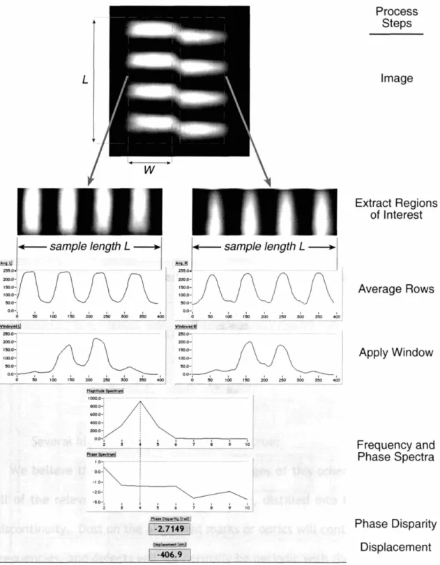
The essential goal of the image analysis is to determine the spatial phase discontinuity between one or more matched pairs of interference fringes. In this section we describe the procedure for the case of a simple pair of fringe sets, and then in Section 3.4, the variations required for a wide capture range.
An image is transferred from a CCDto a framegrabber and from there to computer memory. Two regions of interest (ROI) corresponding to each set of fringes are determined by the operator, and extracted from the image (Fig. 3-1). The sample length L is equal to the length of the region extracted from the image. The width W is selected to avoid overlapping fringes near the interface of the fringe sets. Assuming that there is no azimuthal angle between the
mask and wafer, and that the camera pixel rows are aligned to the fringes, the situation is rather straightforward:
Process Steps Image Extract Regions of Interest
~.J--=-
s:mPle length L --200.0-1 1:50.0- 100.0-:50.0.,..r--
sample length L--:::1--
-- -
-1:50.0-,I::]
o.o-t I I 2001..2, .... I Y~I'\ ..:v.. o :50 100 1:50 <~ 300 ~ ~ Average Rows Apply Window Frequency and Phase Spectra 10 't'tndovtdld ~.o-.---2OO.oJ 1:50.0-' 100.0-' :50.0-' 0.0-~ I I ~ I .~ft .:... o ~ 100 1:50 200 .~ 300 ~ ~ ~ IOOOOT 9000-1 6000-1 400 OJ 200.0I 00-2 1.0 't'_vtd U ~.ol 200.0-1::;J
:5O.oJ I O.O-j o 10Ph... Dis... Il"(r od)I
I-2.7H9
I
Dis.I_t (nm~
I -406.9
I
Phase Disparity Displacement
Figure 3-1: Steps in the phase detection algorithm with fringes aligned to CCO pixel
rows and no angular misalignment between mask and wafer.
First, the pixels in every row parallel to the fringes are averaged. If the sample length L is not an integer multiple of the period of the interference fringes P, then a frequency-domain analysis gives an erroneous value for the displacement x, unless the phase (jJ
=
O. In order to extract an accurate value ofx
for arbitrary values of (jJ it is necessary to eliminate the frequency-domain artifact. The standard procedure for doing so is to apply a "window" to the sample, which smoothly tapers the ends of the sample to zero. In this way there are no sharp discontinuities at the ends of the sample to introduce fictitious spatial frequencies. The frequency-domain analysis then outputs frequency and phase spectra. The value of the phase spectrum at the frequency peak determines the spatial phase discontinuity of the fringes. The phase measurement is converted into a displacement according to the formulasand
Several highly beneficial advantages accrue:
• We believe that one of the major advantages of this scheme is that it uses all of the relevant information in the image, distilled into the spatial phase discontinuity. Dust on the alignment marks or optics will contain higher spatial frequencies, and defects will not normally be periodic with the same frequency as the fringes. Since a single, predictable spatial frequency is selected when picking out the spatial phase difference this excludes contributions of every
other, spurious spatial frequency. This is believed to be more robust than an edge-detecting approach used in many alignment schemes since all pixels of the image contribute to the measurement, not just those in the vicinity of edges.
• The algorithm can be used effectively for both coarse and fine alignment. • The algorithm is relatively simple to implement and code, and in fact can be coded using a few off-the-shelf software components. LabVIEW [6] code is shown in Fig. 3-2.
OJ
1 [0..2]
IDisplaetmtnt (nm)1
LI~nl__:i
Figure 3-2: LabVIEW spatial phase detection algorithm.
3.2 Non-Integer Fringes
It will be instructive to take a closer look at the issues presented by a non-integer number of fringes within the sample length. Without windowing the input sample, errors will arise in two situations: during variations in the sample length, and in the position of the fringes within the sample.
To examine the effect of the number of fringes within a sample, the difference between a simulation of detected and actual phase is plotted in Fig. 3-3, with and without windowing. In the case without windowing, periodic phase errors are evident, amounting to -0.1 radian. For gratings periods P1=
1.00 ).tmandP2
=
1.02 ).tmthis corresponds to an error of 4 nm.234 5 678 Blackman-Harris Window
\
' ~ \ , \ , I,
,.' !\ /'"
No Windowing:: :V
.~ ::..
'. • • , : • I. I • I'. : I •• , :/ \.:=U',. ./
j:', ...
i ,'"', /\-. /: .', " 0.4 ~ co-=-
0.3 Q) en CO ..c 0.2 a. :-ffi 1U 0.1 0. en ~ Q) 0 t5 Q) CD 0 -0.1 I CO :J t5 -0.2 ~ -0.3 0 # Fringes in SampleFigure 3-3: Simulated disparity between actual and detected phase as a function of
the number of fringes in the sample, with and without a window.
In contrast, when windowing is employed the phase measurement error is zero (within 1 milliradian) for more than 1.5 fringes in the sample. This corresponds to an error of less than 0.1 nm. We consider this an indication that the algorithm that determines alignment is capable of true sub-pixel resolution.
Now consider the position of the fringes relative to the extracted regions of the image. The positions of the ROI are specified initially by the user, and remain the same thereafter. Thus we expect an error, if any, to be systematic: non-windowed measurements will be precise, but not necessarily accurate. Figure 3-4 shows the simulated variation in the detected alignment when the two ROI are shifted in parallel, in a direction perpendicular to the fringes. 470" "r ,--,- .-, T ' -, , • ,-' • ,-, I ' T • 'I 460 - ...
-
.... 1/\,
E
,
,
.s
450 - \ 1 No Windowing C 1 \ Q) 1 \ ,.. E 440 - I \ C I \ 0>I
\«
I \ I 430 - I \ -"'0 Q) 1 Blackman-Harris Window \-....
U 1 \' Q) 420 - I....
Q) 1 0 / (a) 410 "/- / (c) 400 L ' o , , , I , 10 , I , , 20 I , , 30 40 , .J 50 (b) Shift (pixels)Figure 3-4: (a,c) Images of the same fringe pattern with the ROI shifted by 40 pixels.
(b) Simulated errors in detected alignment due to the position of fringes with sample
regions of constant length shifted in a direction perpendicular to the fringes. The
error is periodic and can be >50 nm. Windowing reduces the error to <2 nm.
If windowing is omitted, systematic errors of more than 50 nm may result. Using a Blackman-Harris window reduces the possible error to less than 2 nm. Experience with a variety of other windows suggests that this error can be reduced to <1 nm with optimization of windowing parameters.
3.3 Mask-Wafer and Camera Angle
Two important parameters are the azimuthal mask-wafer angle and the camera-fringe angle, either of which will distort the alignment measurement if only one ROIis used for each fringe set, as in Section 3.1. In the general case, a finer-grained analysis is required. Figure 3-5(a) shows eight ROIof width W within one fringe set. The phase-detection algorithm described in Section 3.1 is applied between pairs of these small regions. For example, starting at the leftmost ROI we find the phase between the first and second regions, then between the first and third, and so on across the fringe set. This procedure yields a series of phase measurements from which we can find the phase slope. Continuing to the other side of the mark, the phase slope of the complementary fringe set is determined in a like manner. If the two fringe sets are found to have an equal slope, then we can conclude that they are due entirely to the angle between the fringes and the pixels of the CCDcamera.
w
-ji-i j (a) ~...
....
-~
(b)Figure 3-5: (a) Image of fringes at an angle with respect to the CCD camera. (b)
Chevron pattern resulting from mask-plane angle between mask and wafer.
Alternately, Fig. 35(b) shows fringes with equal angles, but opposite signs -what we call a "chevron" fringe pattern, indicating an in-plane rotation between the mask and wafer. This angle can be eliminated by alignment at two widely separated marks.
In general, we take the difference in phase slopes from the two fringe sets to remove the contribution from the azimuthal mask-wafer angle and reveal the remaining angle due to the camera. The camera slope can be removed in software, or by adjusting the angle of the camera in its mount.
3.4 Wide Acquisition Alignment
The algorithm described here follows a three-tiered approach (Fig. 3-6) to achieve a wide acquisition range - the three regions of the alignment mark shown in Section 2.4 are analyzed from coarsest to finest resolution.
(c)
Figure 3-6: (a) Image of wide acquisition range marks. (b) Bar marks. (c) Coarse
moire marks. (d) Fine moire marks.
Starting with the bar marks, Fig. 3-6(b), we note that alignment is indicated by the position of the center bar between the bars on both ends. An algorithm takes a slice of the mark perpendicular to the bars, fits a gaussian to each peak to find the best-fit center, and takes the difference between the interstitial spaces to determine alignment (Fig. 3-7a). With the bar marks the
acquisition range is as wide as the spacing between the outermost bars (several tens of microns) and the resolution is about 0.5 J-lm. Figure 3-7(b) shows a plot of the alignment repeatability for several hundred iterations of the alignment algorithm. Note that the variation in detected alignment did not exceed 0.5 J-lm. 174.0 160.0- 140.0- 120.0- 100.0-(a) 80.0 60.0- 40.0- 20.0-3.0-1 0.0 I 25.0 I 50.0 1 75.0 **peaks foun I 1 1 100.0 125.0 150.0 Locations ~o 11136.76 1170.23 11102.76 eak di threshold ~125.00 I 642 " ~ - -" I - --5.0-. 964 5.0- 4.0- 3.0- 2.0- 1.0-(b) 0.0- -1.0- -2.0- -3.0-
-4.0-Figure 3-7: (a) Intensity distribution of a slice through a bar-mark image. The units of
the vertical axis are pixel intensity (B-bit digitization). (b) Plot of the repeatability of
300 coarse alignment measurements. The units of the vertical axis are microns.
Within the 1-Jlm range we examine the coarse moire mark. Depending upon the number of fringes in the mark, we use either spatial phase detection or a correlation of the position of peaks, akin to the bar mark algorithm. A comparison of the peaks from two fringes, such as those shown in Fig. 3-7(b), in conjunction with a calibration of the pixel size, gives a resolution better than 0.1 Jlm. The boundary between the phase and peak-detecting regimes is defined by the phase errors associated with fewer than 1.5 fringes. In the final stage, a spatial phase algorithm analyzes the fine moire fringes.
3.5 Speed and Efficiency
To use1661 on a true site-by-site basis for industrial fabrication, it must be capable of ttrealtime" operation, Le., the images are analyzed as fast as they can be transferred from the CCD(1/30 sec). However, for developmental purposes we have chosen to implement the algorithm in LabVIEW. The complexity of the algorithm is sufficiently low that it may be ported to other platforms with relative ease. We make no claim that this is the most efficient implementation of the algorithm, only that it is supremely flexible and acceptably fast for our present laboratory needs. On a 300 MHz G3 processor, the time required for the image transfer and execution of the algorithm is about 400 ms. Once the image is digitized by the framegrabber, the transfer of
the image data to the main computer memory over a 46 MHz computer bus represents a significant fraction of the latency time. A commercially available dedicated DSPprocessor [7] with on-board framegrabbers is expected to be capable of analyzing the images in realtime.
CHAPTER 4:
ALIGNMENT AND X-RAY EXPOSURE SYSTEM
4. 1 System Architecture
A custom alignment and x-ray exposure system (Fig. 4-1) was designed and constructed in the MIT NanoStructures Laboratory for the purposes of exploring and developing 1661 alignment. As discussed in Chapter 2, a predecessor alignment scheme to 1661, called On-Axis Interferometric (OAI) alignment matched the spatial phase of an interference pattern to a set of fiducial marks etched into a wafer. Although the OAI scheme was demonstrated to be sensitive to better than 10 nm, one of the primary constraints of the system was the inability to observe alignment during exposure. This was exacerbated by the fact that the mask/wafer stage assembly was rolled on tracks between the alignment and exposure positions. Mechanical disturbances encountered in moving the stages between alignment
and exposure positions often made good alignment irrelevant. In the present alignment system, care was taken in the system design to permit alignment at
any time - before and during exposure.
Figure 4-1: IBBI alignment and exposure system.
Figure 4-2 is a schematic of the alignment/exposure system, which we refer to as Head 41
• This system consists of a wafer stage capable of positioning
Si wafers up to 8" diameter in X, Y and 0, ,a 6-axis mask stage utilizing closed-loop piezos for mask translation and DCservos for angle and gap control, three IBBI microscopes (necessary to measure alignment in X, Y and 8), a helium enclosure containing a viewport through which alignment is observed during x-ray exposure, and an electron-bombardment CUL-linex-x-ray source (A
=
1.3 nm). When loading the mask, the x-ray source can be raised or moved laterally by a pair of cross-roller bearing linear motion stages [8]. The stainless-steel superstructure is designed for maximum symmetry to ameliorate the effects of thermal expansion, and to provide a structure with high resonant frequency.An Apple Power Macintosh 9500/G3 running at 300 MHz controls the set of servos and piezos. The video streams from the microscopes are digitized using National Instruments PCI-1408framegrabbers. LabVIEW4.1 software is used for image acquisition, analysis, stage control, and exposure control. A third-party image analysis software package [9] is used in conjunction with LabVIEW for the image analysis subroutines. An IEEE-488.2 (GPIB) board completes the interface from the computer to the peripheral stage and piezo controllers. During the x-ray run critical parameters such as the oxygen level, and current and voltage of the HV power supply are continuously monitored by
1Head 4 is the fourth in a series of x-ray sources constructed in the NanoStructures Laboratory.
the computer through an analogI digital I10 board [10]. Solenoids controlling water and helium flow are also controlled through this board.
Vacuum Chamber
X-ray Point Source
Ion Pump
,--
---,I I
I Mask Stage
I
:
Helium Enclosure.i,
:=
====================L
i:L
Wafer StageJ
Newport Vibration Isolation Table
9S00/G3 PowerMac Framegrabber Framegrabber Video A&D I/O GPIB Newport PM-SOO Motion Controller Queensgate Digital Piezo Controller Varian
StarCell Ion Pump
Delta F Oxygen Sensor
Spellman HV Power Supply
Figure 4-2: Schematic of alignment/exposure system. The multitudinous connections
between the components are not shown for clarity.
The operation of the system is as follows: Prior to an exposure the mask is loaded with the x-ray source in the raised position and the top of the helium enclosure removed. The front of the helium enclosure is removed to allow the wafer stage to slide out from underneath the mask stage. After the mask and wafer are loaded, the x-ray source is lowered into position, the helium enclosure is sealed, and the 1661microscopes are brought to their observation positions. Alignment is performed with all components in place. The path between the mask and source may be purged with helium either before or after alignment. At this point the exposure is initiated. Alignment is monitored throughout the exposure, and small corrections made as necessary. The system assumesan x-ray source that operates vertically, although the basic principles of the system can be adapted to a source which operates horizontally, e.g., a synchrotron.
4.2
X-ray Source
We choose to use x-ray lithography as the test vehicle for 1661alignment since it has many advantages over competing exposure schemes, such as absence of spurious scattering, large process latitude, good resolution, and high throughput. Due to its history, numerous advantages, and research successes,it is not an exaggeration to say that it is the leading contender for
the dominant semiconductor manufacturing technology in coming generations. One of the primary reasonsfor this is that x-rays have the unique property that spurious scattering is negligible, due to the fact that the real part of the index of refraction is very close to unity for all materials. In contrast, ultraviolet (UV) photons undergo significant scattering, as do ions near the ends of their trajectories. Such spurious scattering causes exposure in regions where it is not wanted, so-called proximity effects. Absorption without spurious scattering is certainly one of the main reasons for pursuing x-ray lithography, especially for nanolithography.
In the NanoStructures Laboratory we use a low-cost electron bombardment x-ray source with a copper L-line wavelength (A=1.3 nm). Figure 4-3 shows the pertinent parts of this source.
A tungsten filament is held at 8 kV below the potential of a grounded copper anode. A current is pulled off the filament and the electron trajectories follow paths from the circumferential filament towards the center of the copper target. Focusingis achieved by sliding the assembly holding the filament along its axis.
Tungsten Filament (-8 keV) Water Cooling A = 1.3 nm ~hV
/~:'7
Copper Target I I IFigure 4-3: Photograph of an electron-bombardment x-ray source. A tungsten
filament is held at 8 keY below a copper anode. Electrons pulled off the filament
impinge on the center of the copper target. Moving the filament relative to the anode
focuses the electrons. The CUL-line has a wavelength of 1.3 nm.
The entire assembly is held in vacuum, typically at about 10-7 Torr. X-rays traverse the distance to the mask (250 mm) through regions of vacuum and atmospheric-pressure helium, separated by a 1.6 J.,lm-thick silicon nitride vacuum window held on a polished o-ring mounting in the bottom of the vacuum chamber. The diameter of the vacuum window is 20 mm.
Once the electrons impinge upon the copper target they undergo collisions which generate x-rays and many secondary effects, such as heat and electron emission from the target. One strong x-ray line is produced at 1.3 nm and there is background radiation from bremstrahlung. A photograph of the x-ray source in operation is shown in Fig. 4-4.
Figure 4-4: X-ray source in operation. X-rays are emitted downward into 4n
steradians.
The probability that x-ray emission will occur rather than an Auger electron being ejected is called the fluorescent yield of the material. For the
CUL line the fluorescent yield is only 0.006. This means that the copper target
is not very efficient at generating x-rays. Given the inefficiency and consequent long exposure times of an electron-bombardment source, one may wonder why we use it. For the relatively modest requirements of a university laboratory, the x-ray flux from a CUL source is adequate. Furthermore, it is
compact and relatively inexpensive. When high throughput is a necessity, as in industrial production, synchrotrons or other sources can be substituted.
4.3
Nano-positioning Stages
To take advantage of the powerful combination of IBBI alignment and x-ray lithography, several requirements based on the needs of the lithography must be met. In order to understand these needs, we will briefly describe the principles involved.
In proximity x-ray lithography a mask is held at a microgap to a wafer coated with resist, as shown in Fig. 4-5. This mask has an absorber pattern that is a high-Z material, such as gold or tungsten. The 200-nm thickness of the absorber is designed to give a 10-dB attenuation. The mask-wafer gap determines the minimum feature size for a given wavelength of illumination. Linewidth consistency demands that the gap is consistent over the entire mask - thus, mask flatness is critical.
kinematic
mounting
absorber
incident x rays
wafer
G, gap
membrane
frame
Figure 4-5: Schematic of mask and wafer. Photosenstive resist is patterned by
exposure with x-rays following selective patterning by mask. Due to diffraction
limitations, the gap G determines the finest possible printed feature.
Diffraction in the gap between the mask and wafer is the only important consideration in evaluating resolution since the effective range of Auger electrons is only about 5 nm. The relationship between gap, G, and the minimum printable feature size is given approximately by
where a is a scaling parameter (the reciprocal of the square of so-called Fresnel number), Wmin is the minimum linewidth, and A is the source wavelength. Analysis and experiment show that a values of 1 are permissible for high quality pattern replication, and values of 1.5 yield good process latitude [11].
Figure 4-6 illustrates a plot of the maximum allowable mask-wafer gap as a function of the minimum linewidth for a wavelength of 1.3 nm and a
=
1, 1.5, and 3 respectively. 250 200J<=
1.3 nm 150 100 . . . .. .. .... .. .. ..... .. .. .. .. .. ...... .. .. .. ... .... .... .. .. .. .. .. .. .. ... .. .. .... .. .... .... 50 o o 50 45 .aW
2
G=
40 .A
35 .Minimum
linewidth,
W (nm)
Figure 4-6: Plot of the maximum allowable mask-wafer gap as a function of the minimum linewidth for a source wavelength of 1.3 nm and a. = 1, 1.5 and 3, respectively.
As we can see from Fig. 4-6, for sub-50 nm features, the maximum
allowable gap is <10 ~m. At this gap of a few microns, physical contact
between the mask and the wafer is possible, but should be avoided to preclude
damage to the mask or wafer. However, 3 ~m gaps are achieved routinely on a
laboratory bench in a Class 10 cleanroom in the NanoStructures Laboratory,
although the mask motion is constrained by hydrodynamic effects [12] at gaps
below 10-15 J.tm.
The resolution limit of x-ray lithography2 can be reduced to the question
of what is the smallest practical mask-wafer gap. Two requirements are apparent: the mask and wafer must be optically flat, and no dust or particles can be allowed on either surface, or else they will distort the gap.
(b)
(a)
Figure 4-7: (a) MIT x-ray mask structure. (b) Interferogram showing mask membrane
flatness.
The mask design used in the N5L is shown in Fig. 4-7(a). The 5i-rich, low-stress silicon nitride mask membrane is supported by a silicon annulus, which is anodically bonded to a Pyrex ring. The purpose of the mesa is to allow
2 For the moment we are setting aside the resolution limits imposed by chemically amplified
resists.