Drawing the Electric
SAMUEL JACOBYAB Computer Science Harvard University 2009
Submitted to the Program in Media Arts and Sciences, School of Architecture and Planning, in partial fulfill-ment of the requirefulfill-ments for the degree of Master of Science in Media Arts and Sciences at the Massachu-setts Institute of Technology.
June 2013
COPYRIGHT MASSACHUSETTS INSTITUTE OF TECHNOLOGY, 2013. All Rights Reserved.
ARCHMES
I MASSACHUSETTS INSTMftE OF TECHNOLOGYJUL
19 2013
LiBRA RIES
Sam Jacoby Program in Media Arts and SciencesMIT MEDIA ARTS & SCIENCES Accepted:
le
-Leah Buechley Associate Pfofessor of Media Arts & Sciences
MIT MEDIA ARTS & SCIENCES Certified:
Patricia Maes Alexander W Dreyfoos (1954) Professor
Associate Academic Head Program in Media Arts & Sciences
Drawing the Electric
SAM JACOBYAB Computer Science Harvard University 2009
Submitted to the Program in Media Arts and Sciences, School of Architecture and Planning, in partial fulfill-ment of the requirefulfill-ments for the degree of Master of Science in Media Arts and Sciences at the Massachu-setts Institute of Technology.
June 2013
COPYRIGHT MASSACHUSETTS INSTITUTE OF TECHNOLOGY, 2013. All Rights Reserved.
Abstract
This thesis explores the intersection of craft and electronics by way of paper and conductive ink, a domain that I'm terming papercraft electronics-a syn-thesis of electronics, drawing, and painting. I investigate the nature of making a physical electronic artifact, and the ways in which that making informs our relationship with both the artifact, specifically, as well as technology writ large.
I examine craft-the manual process-as a means for embedding new kinds of
personally-significant meaning in electronics, re-positioning electronics fabri-cation as the creation of personal, unique, hand-crafted artifacts.
I do so through a series of case studies oriented around the papercraft elec-tronics domain. Through a sequence of projects, workshops, and evaluations,
I examine the personal connection and pride that comes with making, as well
as the handmade artifact's place in technology. In particular, I initiate projects around the making of paper sensors, speakers, synthesizers, and audio-aug-mented artworks.
Thesis supervisor Leah Buechley
Drawing the Electric
SAM JACOBYREADER Mitch Resnick
LEGO Papert Professor of Media Arts & Sciences MIT MEDIA ARTS & SCIENCES
Drawing the Electric
SAM JACOBYREADER Joe Paradiso
Associate Professor of Media Arts & Sciences MIT MEDIA ARTS & SCIENCES
ACKNOWLEDGEMENTS
Many thanks to Leah Buechley, for all of her guidance, and to Mitch Resnick and Joe Paradiso for their help and assistance. Thanks, also, to my fellow students in the High-Low Tech group. A special thank you to Brian Mayton, for all of his patient explanations. It's been a gift and privilege to learn from all of you.
Contents
1 Introduction 13
Making 13
The Problem with Making Electronics 14 Crafting Electronics 16
Case Studies 17
2 Related Work & Background 19
3 Materials & Processes 23
Material Practices 24 Processes 25
Assembly 27
Challenges 30
4 Paper Sensors 31 5 Microcontrollers meet Paper 43
Papercraft and Programming 43
TinySynth 50 6 Paper Clips 65 Design Process 65 StoryClip 66 TouchSynth 75 7 Findings 80 Lessons learned 80 Making meaning 81 Future Considerations 82 Conclusion 83 References 84
Chapter 1
Introduction
Over the last several years, no products have pushed more-muscularly into our lives than those associated with technology. Computers have become universal, sensors ubiquitous. Everywhere, our experiences are mediated by a layer of electronica; a buzzing slice of ether that constantly informs, twitches, and beeps. Our lives-as they are lived-are governed by a teeming ring of devices that are difficult, if not impossible, for any one individual to fully understand. How could we? Our prod-ucts are the end-points of sprawling industrial networks, the terminators of globe-spanning manufacturing and knowledge chains. The role of the person, the single user, is vanishingly small.
It is not my intention to reclaim industrial production for the individual, nor rollback the boons of an increasingly-interconnected world. Instead, I will focus on the making-and-understanding gap-the chasm between that which we use and that which we can make and understand. I will argue that individuals' engagement in making is a critical to our understanding of how we use and interact with technol-ogy. In this thesis, I will investigate the act of making through the lens of papercraft electronics, focusing on both the expert and the novice practitioner. Through a se-ries of case studies, workshops, and curated experiences, I will argue that to create is to understand, that to rediscover the essential creative qualities of the handmade in technology, is to feel agency and control over it.
1.1
Making
To make is to create something physical with your hands: a tangible, seizable, break-able thing. It is to unmask and expose the workings, to make is to make something
special, embedding it with a kind of singularity. The process of manual construction engenders an intimacy with ones' tools and with ones' body, fostering a creative and flexible process open to detour and discovery. To make is to acquire knowledge-it is to create in the most primordial of senses.
The handmade artifact is something unique and personal, having a quality both familiar and difficult to articulate: a feeling of comfort, of touch, a feeling of the weathered and the worn. It's a quality shared by the walking stick and the century-old violin, as well as the thrown pot and the wrought-iron gate. It is shared, also, by the casually-scrawled postcard, the thumbprint, the erasure, the footprint in sand. These are the marks we-people-make, signifiers of our presence, as well as evi-dence of immediate, manual involvement. These are qualities that are by and large, absent in electronics.
1.2 The Problem with Making Electronics
Our technologies are reflections of the aesthetics of our age: all is milled aluminum, glass, plastic, meeting in mirrored perfection. As our technologies streak towards an engineered apotheosis, they become more foreign and more opaque. Capturing the embodied qualities of the handmade for electronics is not easy. Indeed, few classes of artifacts are more resistant to such treatment. The latest iPhone, marvelous though it may be, might as well be extraterrestrial. Considering that the utility of such a device is commensurate with its engineering, there is little hope for the individual to make much headway in reclaiming commercial electronics as "handmade".
The intention here though, is not to argue against mass-manufactured electron-ics. It is only to acknowledge that a spectrum of essential human experiences are lacking in the making of technology as currently conceived. The making process
is an important part of our relationship with the built environment, and craft and craft-processes are a way of re-introducing the agency, pride, and ownership that comes with the self-made.
The importance of that process has been increasingly recognized. The rise of communities of independent makers, the knowledge-exchange and sharing enabled
by the internet, and the increasing availability of parts and materials through online
distributors, have made the do-it-yourself (DIY) and maker communities more rele-vant and capable than ever [18]. By honing in on papercraft electronics, formulating a set of projects and ideas, and guiding novice and expert-makers through the pro-cess, I hope to shed light on the nature of the relationship between the handmade, the maker, and the technology that surrounds us. I also hope to provide the
be-ginnings of an educational approach to such technologies, giving them some place in the broader effort to make electronics and technology-education more accessible and diverse.
1.2.1 Definitions
In exploring these subjects, I will be investigating questions that are unique less in their substance, than in their contextual framing. For this reason, it is important to define terms that have multiple valences of meaning.
Handmade
First, what is the handmade? Examining the handmade production of goods in a craft context, requires examining the broader nature of the handmade goods. Be-cause of low-cost labor in many countries, a variety of commercial products are, to one degree or another, handmade. And many sophisticated devices require some degree of manual labor, whether it is in soldering through-hole components, wrap-ping magnet wire, or feeding parts through assembly tools. Such work, skilled though
it may be, is not what we mean, when we discuss the handmade. It is a question that others have grappled with. Etsy, the online-marketplace for crafted goods, has approached the question in an interesting way. It only permits companies of two-or-less people to sell products online, preventing the flood of low-value, mass-produced, "handmade" products.' In our context, we can be somewhat less obtuse. I will discuss the handmade in fairly general terms, meaning a unique, tangible, de-vice that is created by an individual.
Papercraft Electronics
Much of the work in this thesis is oriented around what I've been calling paper-craft electronics. In some sense, this is a misnomer-paperpaper-craft is a term most often used to describe elaborate paper models-not the simpler paper constructions in the projects described in the following chapters. All the same, it is important to distin-guish such efforts from paper electronics, which can be conflated into a broad range of devices, including e-ink screens, and other electronics whose primary focus is on flat, flexible, inexpensive electronics. Such subjects are of no doubt great inter-est here, but they are not my chief focus in initiating and exploring these subjects.
Papercraft electronics, in this context, refers to devices made of conventional elec-tronics constructed on a standard, porous, paper substrate. Typically, this involves adhering surface-mount or through-hole components to the sheet using conductive ink or epoxy.
1.3
Crafting Electronics
To craft electronics is to make electronics in a way very different than the way in which we we expect. Prototyping on a breadboard, soldering on a protoboard, or having a printed-circuit board (PCB) fabricated, while well-proven, make use of a narrow range of techniques and materials that are optimized for reliability and industrial production. As the range of what we consider to be raw materials for electronic construction expand, though, so do the ways in which we make them. New materials bring new ways of making. An electronic device that incorporates bananas is grown as much as it is made, and a wall of responsive pigments can be painted or drawn. Crafted electronics can be folded, carved, plated, or sketched [25]. While the materials and the techniques are important-other facets of crafting are more relevant to this thesis. With changing ways of making, come changing rela-tionships and changing perceptions. Something prized out from between styrofoam sheets is a very different thing than the same plucked from a tree, or found under a pile of leaves. These perceptual differences give entry to a new range of relationships with technology-relationships in which the creative role of the maker is paramount to the experience of the end-user.
With craft, also, comes a synchronization of hand-and-mind, a pleasure taken in mark-making and pride in ownership and creation. It also creates a different kind of artifact: something fragile, human, and unique, products of what David Pye has termed, the "workmanship of risk,' artifacts created by the free hand, open to imperfection and failure [28].
By embodying such craft practices in the creation of a physical device, I hope to
not only cultivate a sense of personal connection and pride in a user's relationship with his or her tools, but to recontextualize technology. A device need not only be a means to manipulate a software application, but a personal expression of a user's relationship to their praxis, and an exemplar of the creative impulse in its own right.
I hope to raise consciousness of the diversity of modes in which technology can be
produced, and the importance of re-situating technology-making in the purview of craft.
In this thesis, I will argue that a personally-crafted device is a personally mean-ingful one. It leverages our capacity to manipulate the tangible, to draw and to make, to fabricate our world, giving us agency to create the technology that increasingly surrounds us.
1.4
Case Studies
Over the course of the next five chapters, I will describe a series of projects, work-shops, and experiences, that examine the relationship between making, papercraft, and technology. Each explores a facet of papercraft electronics and conductive inks, whether it be technical, experiential, or creative. Through these studies, I have two goals: first, to define a design-space for papercraft electronics, and second, to share those designs and processes with groups of people, evaluating their experiences, and understanding how it might inform their broader relationship with technology.
In identifying key areas of interest, I focused on functions that interested me personally and that I saw as opportunities for others to engage in making
paper-craft electronics. Whether it was in making sensors, as in Section 4, or music, as in Sections 5.2 and 6.3, introducing reprogrammable microcontrollers to papercraft, as in Section 5.1, or creating tools for interactive illustration and storytelling in Sec-tion 6.2, each project sought to present a cross-secSec-tion of the design space. Details
are given below:
Paper Sensors (Section 4) consists of a series of capacitive and resistive sensors, handmade on paper. It explores some of the affordances offered by analog electronics, coupled with papercraft and conductive inks. It also examines robust techniques for fastening components to paper surfaces and painting regular, reliable, conductive traces.
Papercraft and Programming (Section 5.1) is a series of techniques and tools for working with microcontrollers, conductive ink, and paper. This work was carried out in conjunction with David Mellis, Leah Buechley, Hannah Perner-Wilson, and Jie Qi, in TEI 2013 [21].
TinySynth (Section 5.2) is an eight-bit four-voice digital synthesizer, built with a handful of components on a piece of paper. It takes ideas developed in "Pa-percraft and Programming" to motivate more complex integrated electronics made with conductive ink.
StoryClip (Section 6.2) is a software-hardware package that allows you to record sounds associated with specific conductive regions in a drawings. It is the first iteration of a clip-on capacitive-touch sensor board for adding functionality to conductive drawings. It permits conductive regions in a page to be associated with specific sound recordings.
TouchSynth is an extension of the original StoryClip design, but with many modi-fications made after an initial round of workshops. It is a stand-alone battery-powered clip-on capacitive sensor, with an onboard speaker and amplifier. It is intended to allow for StoryClip-like affordances in more diverse and varied settings.
In the chapters to follow, I will examine these projects in turn, first, tracing over related work and background in Chapter 2, then the general materials and processes used in all case studies in Chapter 3. After that, I will discuss my work with Paper Sensors in Chapter 4, Microcontrollers in Chapter 5, and auxiliary clip-on boards in Chapter 6.
Chapter 2
Related Work & Background
The space surrounding papercraft electronics is rich, ranging from user-interface and user-experience design, to examinations of novel electronic substrates and man-ufacturing methods. In pursuing the work here, I intend to draw upon a cross-section of prior work.
This thesis owes a particular debt to a key set of investigators: Hannah Perner-Wilson, Jie Qi, and Leah Buechley, in particular, have pioneered many of the tech-niques and practices that come into in play in subsequent chapters ( [25], [29]).
E-textiles
Of particular relevance is the domain of e-textiles, which has presaged the progress
made in papercraft electronics, integrating, as it does, electronic components with conductive threads, fabrics, and other soft materials [20]. Work with e-textiles has provided a rubric of challenges and questions that have informed this thesis [1]. The Lilypad Arduino project, in particular, has served as great inspiration, by articulat-ing a series of tools and techniques organized around a specific material domain [2]. In [26], the authors describe a set of techniques for creating textile sensors using a range of conductive materials and craft techniques, which serve as an inspiration for the Paper Sensors (Section 4) here.
I've drawn personal inspiration from the ability of e-textiles to merge electronics into artifacts whose aesthetics are shaped by their textile and craft components and to engage different skills and groups than other forms of technology construction. The value of this integration of craft and technology is discussed in more detail in [5].
2.0.1
Other Materials
The ambition with which researchers have explored other functional materials has opened up many doors in examining the kinds of materials and material practices that might be suitable for this investigation. In [15], the authors discuss methods for rapidly creating interfaces from cardboard, tinfoil, and pushpins. Squishy Cir-cuits [16] is a technique for creating electronic cirCir-cuits with conductive and insu-lating play-dough. Researchers have also explored hacking and re-using of existing electronics-a practice rich with research potential, and an inspiration for Synth projects in Chapter 6. For example, the practice of circuit bending [14] encourages people to hack existing musical devices in order to create new interfaces and sounds, and the Scrapyard Challenge [22] series of workshops encourages participants to reuse existing objects to create interfaces for musical control.
Technical Background
While this is not a technical thesis, it draws on the work of a great many mate-rial scientists, electrical engineers, and tinkerers. Much of the work is made possi-ble by the growing availability and refinement of a broad assortment of conductive paints and inks. Advances in conductive inks and drawable electronics [33] have opened up new fronts in creative technology design. Such materials have enabled new form-factors for interaction and new methods of technology-making. The op-portunities that such materials present in creativity and learning-particularly in a craft context-are many [10].
Teardrop Microcontrollers
For instance, Teardrop microcontroller kits provide deep flexibility while working with paper and conductive inks, allowing for a synthesis of embedded computa-tional elements and paper-based arts [3]. Teardrop introduces programming and circuit design while allowing for creative expression with unconventional materials. While we've chosen to emphasize a less kit-oriented approach, Teardrop remains a touchstone of paper-based electronics and subsequent research.
Conductive Inks
Various facets of painted and drawn circuitry have been explored by others and in-form the work here. Conductive paints and integrated electronics have been used in creating responsive wallpapers and interactive pop-up books, both predecessors to
the projects articulated in the chapters to come ( [30], [4]). Graffiti Research Lab has done multiple projects using conductive paint and other materials to create circuits on walls and other surfaces. 1 Perner-Wilson describes many different approaches
to the integration of craft and technology, including the use of conductive paint on various substrates [25].
Paper Electronics
A wide-range of academic work has explored the integration of electronics and
pa-per. From an industrial perspective, there has long-been an interest in paper elec-tronics, as a cheap, light, flexible, and highly-manufacturable substrate [38]. Ad-vances in that domain have traditionally come from the increasing miniaturization of silicon chips and new manufacturing techniques. Much of the relevant work in this area has involved putting commercial and academically-developed inks to new use, and to developing techniques for integrating such materials smoothly into a craft context.
Coelho et al. [7], in particular, has shown a series of techniques for embedded electronic components into hand-made paper and creating circuits with conductive inks. Saul et al. [34] describe a set of technological paper artifacts, including small robots with circuits made from gold-leaf. Russo et al. [33] describe a conductive ink pen they've developed for drawing circuits on paper. Qi and Buechley describe a set of artistic artifacts made using paper circuits [31]. Paper as a medium for rapidly prototyping tangible interactions [39] and for creating interactive devices [13] have also been wellsprings of information and ideas.
Such efforts have principally focused on new techniques for working with con-ductive materials, and on the production of novel artifacts-and somewhat less on creating contexts for creative expression and personally-meaningful engagement, that I will be examining in large measure here.
Interactive tools for children
This thesis has also been motivated by a set of richly-interactive tools that create new interactions with sound, drawing, and art. Many have focused on children. A number have leveraged the natural resistivity of pencil-graphite as a means of sound-generation ( [35], [6]). Jabberstamp allows children to make use of conventional art materials, using a device that maps sounds onto digitally-tracked stamps using a WACOM tablet [32]. MaKey MaKey uses an auxiliary board and resistive sensors
to allow a diverse set of materials to be incorporated into devices [8]. MaKey MaKey is a close kin, in particular, to the TouchSynth and TinySynth projects (Sections 5.2 and 6.3, respectively). It is worth noting that MaKey MaKey makes use of different technologies and prioritizes different design modalities, namely, easy-integration with a computer and keyboard-emulation.
A considerable amount of research has explored the affordances digital
tech-nologies can offer in synthesizing new ways of storytelling and sharing. Most have focused on integrating users'images and recordings into a completely digital medium [12]. Commercial products, like Hallmarks Recordable Storybooks have explored a similar spaces as well.2 Such efforts have been focused more on enriching pre-existing content, rather than on creating one's own.
2.0.2 Onward
In the case studies to follow, the materials and techniques referenced above play a critical role in the design and procedural choices made. Of particular importance are the suite of materials chosen-in this case, conductive silver inks and paper, as well as the techniques and processes to work with them. Both are discussed in the
chapter to follow.
Chapter 3
Materials & Processes
3.1
Material Practices
In structuring this research, we've chosen to focus on two material domains: that of conductive ink and that of paper.
3.1.1
Conductive Ink
Conductive inks are a rich opportunity for the design of papercraft technologies. Recent advances in the manufacture and distribution of conductive inks1have made them widely-accessible, both in research and hobbyist settings [33].
Conductive inks offer untraditional affordances. Melding electronic design with craft techniques, like drawing, painting, and printing, making electronics with con-ductive inks has as much in common with creating art as it does with breadboarding circuits. Conductive inks can augment existing surfaces and structures. Without any native structure, they can adapt to unconventional form factors and unusual sub-strates.
Inks allow for a full range of creative expressivity. Conductive inks can be sketched from a pen, drawn with a paintbrush, or screen-printed on a wall. Such artistic tech-niques permit an intersection of two kinds of making. There is the natural creativity of craft, of mark-making, and of design. But there are also the constraints and affor-dances of conventional technology design. Introducing a functional material into a craft context leverages the strength of the handmade, without fully sacrificing the utility of the technical.
In this thesis, a number of different kinds of conductive ink were used. Conduc-tive Compounds manufactures a wide-range of commercially-available conducConduc-tive ink, and will sell them in (relatively) small 100g sample sizes. Their AG-510 and
AG-530 inks are more resistant to cracking than the water-based WB-101, at least
in my experience, but require a chemical solvent for dilution. All of the inks used are detailed below:
. Conductive Compounds AG-510 . Conductive Compounds WB-530 . Acheson Henkel Electrodag 725A . Bare Conductive carbon-based ink
. Pen-on-Paper flexible electronic silver nano-particle inks 'Bare Conductive Ink (http://bareconductive.com)
Conductive ink pens
While pen-dispensers for conductive ink have been available for some time, they have been of low-quality, targeted chiefly at small circuit and windshield-defroster repair. More recently, conductive inks have been targeted at the hobbyist and maker community, chiefly through Bare Conductive, a UK manufacturer of carbon-based conductive inks.2. While highly-resistive, when coupled with a higher-voltage source e.g a 9-volt battery, LEDs and other papercraft devices can be powered. It is not suit-able for use with a microcontroller without a regulator. Bare Conductive's carbon ink is skin safe, which offers an alternative interactive mode not explored here. It is available both as an easily-applied paint and as a squeezable pen.
3.1.2 Paper
Paper is unmatched in its versatility, affordability, and ubiquity. Nowhere is this more true than in the making of art: an infinite variety of forms can be created with a sheet of paper and a pencil, and the intuitive nature of making a mark on a surface is meaningful and natural. It is not surprising that art supplies are among the earliest tools that children become familiar with. Through the case-studies to follow, we used a wide-range of papers with good results.
Conductive inks perform better on coated, non-porous papers, but such plasti-cized papers do not have the tactility and texture that makes working with paper so intriguing to begin with. For that reason standard light-weight and medium-weight papers were used. Some workshops made use of colorful construction paper, which allowed participants to create new designs with the paper itself. In other cases, and in most of my personal explorations, I used a standard, white 241b paper-stock, ob-tained from a local crafts store. It was stiff enough to be folded into a variety of forms, while remaining legible as a simple sheet of paper.
3.2
Processes
A number of different processes were used to construct the papercraft devices.
Con-ductive ink was applied from a pen, with a brush, or through a mask. Circuits made use of a variety of off-the-shelf electronic components, as well as crafted design ele-ments, like folded-paper battery holders and speaker coils. Many of the techniques
2
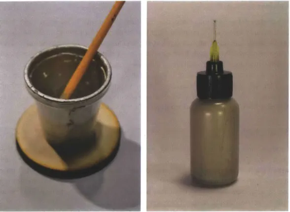
Figure 3.2: Silver-loaded inks to be applied by brush or syringe-tipped bottle.
used were pioneered by others, in particular by Perner-Wislon, Buechley, and Qi in a variety of their works cited above, chiefly ( [5], [29]).
3.2.1
Applying ink from a bottle
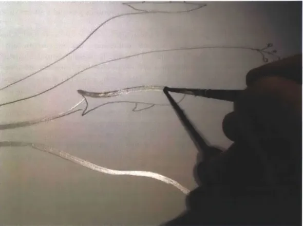
One frequently used method in applying conductive ink is to dispense it from a syringe-tipped squeeze bottle (see Figure 3.2). The bottles offer a good balance of cost, reliability, and control, which are all important in ensuring good conductivity. The WB-101 water-based silver conductive ink, when thinned with distilled water to a 10:1 ink-to-water ratio by weight (e.g. 20 grams of ink to 2 grams of water), flows easily and dries rapidly. The diluted mixture can be loaded into the 1-ounce squeezable bottles and dispensed through disposable 20-gauge syringe tips. So
pared, a line roughly 1mm in diameter can be drawn on a variety of surfaces. After five to ten minutes drying-time, the line has a resistivity of 03 Ohm/cm, which is adequate for circuits constructed on a sheet of letter-size or A4 paper. With care and experience, the process is not so different than writing with a paint pen, or similar implement with a high-flow rate.
3.2.2
Preparing ink for painting
The ink can also be applied with a brush (see Figure 3.1). Most of the conductive
inks available are designed for application in industrial screenprinting and their vis-cosity is tuned accordingly. By mixing them with solvent-be it water or something else-they can be made appropriate for application with an ordinary brush. This introduces a different expressive mode, encouraging free-form application of inks, though, depending on the brush-size, with correspondingly less control. They dry slowly at room temperature, which removes one of the frequent hurdles encoun-tered with the syringe-tipped squeeze bottles, when ink dries in the narrow-gauge tip. It does introduce another issue, in that because they dry more slowly, they re-quire curing to dry completely in a workshop setting.
3.3
Assembly
Applying ink is one thing-making interesting things is another. By integrating electronic components into circuits drawn with conductive ink, more complex de-vices can be made. Common components like LEDs, resistors, and capacitors, can be assembled in a variety of configurations.
3.3.1
Working with Components
In my own projects and in the workshops that we conducted, we used a variety of electric components to construct papercraft electronics:
. ATTiny45/85 microcontrollers . Operational Amplifiers
. 1206 surface-mount package LEDs in a variety of colors * 1206 surface-mount resistors in a variety of values . 2032 and 2016 coin-cell batteries
. N-channel MOSFETs . PC speakers
In addition to the components listed above, I also used conductive copper tape, which is useful for reinforcing papercraft circuits with sharp folds, and magnet wire, to create speaker coils. All of these components are inexpensive, costing a few dollars at most.
Securing components with ink
In creating papercraft electronics, it is essential to be able to reliably adhere elec-tronic components to the paper substrate. This is a challenging task. The stiff metal contacts of surface-mount and through-hole components make an uncomfortable match for soft, flexible, paper. There are a number of tactics available to resolve the issue. Most involve using the natural adhesion of the conductive ink itself to secure the component to the page, using it as means to create traces, as well as a kind of cold-solder to connect electric components to the paper surface. When dry, most conductive inks adhere well to both the paper as well as the metal leads of electronic components, forming durable conductive bonds.
In order to integrate through-hole dual-inline package (DIP) microcontrollers into papercraft electronics, we bend their legs outwards and glue the plastic package directly to the paper. We then trace lines of conductive ink from the legs of the microcontroller onto the paper using the squeeze bottles. Similar techniques apply to components like LEDs or light sensors. We've developed a range of techniques for holding the battery, from securing it in place with a binder clip to attaching a discrete battery-holder.
Using conductive epoxy
In some situations, particularly with thinner inks, or those dispensed from a fine-tipped pen, it is difficult to rely on the paint alone to adhere strongly to both the paper and an electronic component. It was useful to have conductive epoxy on-hand, like that manufactured by MG Chemical4. Conductive epoxy, while rigid and difficult to work with, forms a reliable and durable connection between painted conductive inks and component leads. I found it exceptionally useful in debugging circuits, because it allowed you to focus on elements of circuits that were more in-teresting, rather than focusing on creating reliable interfaces between the inflexible metal leads and the flexible paper. The epoxy does need to be cured, so a toaster oven, hot air gun, or even a hair dryer is necessary.
3.3.2
New Advances
More recent sophistications in the manufacture and design of silver-loaded conduc-tive inks have resulted in a novel class of conducconduc-tive inks that can be dispensed from commercially-available roller-ball pens [33]. While still in their infancy, these inks have a conductivity an order of magnitude greater than that of previous iterations, and permit low-voltage papercraft devices to be sketched and drawn in an intuitive way. Though very easy to apply, such silver ink suffers from many of the same issues endemic to other conductive inks. In addition, it is also difficult to obtain, as it is only manufactured in a laboratory setting. I have done some work with such pens and are excited about the possibilities in the future. Analisa Russo and I conducted a brief workshop at Maker Faire NYC 2012, using conductive pens from the Jennifer Lewis group (see Figure 3.3), and found them intuitive and easy-to-understand, even under demanding conditions.
Figure 3.3: Workshop examples from MakerFaire complete with A. Russo's Pen-on-Paper silver ink. A surface-mount LED is attached at center.
Other recent advances have permitted the ink-jet application ofhighly-conductive inks in off-the-shelf printers, as well as markers on specially-treated paper [17]. Such
tools have enormous potential in this space and in others. The pace of innovation in this arena appears to be ticking upwards, and we anticipate a broad range of ma-terials suitable for paper application in the coming years, with some mama-terials that are now only available in a research setting making their way to market.
3.4
Challenges
Working with conductive inks and papercraft electronics is unlike making technol-ogy in other ways. While technical efficacy is typically prioritized in electronics design, papercraft electronics must address an alternate typology of technological fitness: one that permits users maximal flexibility in drawing and painting, while maintaining as much functionality as possible. The designs in question must there-fore be highly adaptable, auto-calibrating, and capable of maintaining reliable be-havior across a range of use cases.
Figure 4.1: Single-axis papercraft "accelerometer" with proof mass.
Chapter 4
Paper Sensors
As sensors become ubiquitous our awareness of their presence dims. Our devices grow more powerful, making it more and more difficult to understand just how and what they're sensing. Our own senses, that of hearing, of sight, of sound, touch, are more or less clear to us-but what does it mean to detect the wind? What is
vibration? How does an accelerometer work? Creating a context in which such devices' functionality is exposed is something that is not particularly easy. These paper sensors explore the nature of the self-made device, in both its functioning and its efficacy. In so doing, we hope to embed the agency of the maker in the sensing process, turning the abstract concept of environmental sensing, to a very physical and real relationship with the technology itself.
The initial work here establishes a design space for paper-based sensors and em-bedded electronics-not a technical delineation of the space, though that is a cer-tainly critical part of the discussion-but an articulation of the affordances that self-made paper sensors present.
4.0.1
The Self-made Sensor
Such devices are interesting less because of their novel form factor, but because they are functional facsimiles of fully-enclosed MEMS devices. While a MEMS sensor conceals its functionality in its scale, the self-made sensor exposes it in the macro, making-process underpinning its creation.
Additionally, unlike a breadboard prototype, the self-made papercraft sensor cannot be disassembled once made. The conductive epoxy and paint cannot be re-moved, as are the components. The devices are built up through a series of accretive steps, each adding to the next, culminating in a functioning device.
Each addition is small and necessarily limited; a circuit is created by painting a series of marks, each independent, with its own qualities. While in a conventional circuit, a wire is a wire, in papercraft electronics, it is anything but: it is a line, a mark, a smear, or something else altogether. What is of particular interest in these paper devices is that the crafted element is not simply one of connecting various electronic parts. A large portion of the functional components of the sensors themselves are drawn. A wire is not plugged in, but drawn in a series of steps. Once the components are added, they too, are final, losing their repeatable and reusable properties, and becoming part of the whole. The constructive process by which the sensor is built captures something of the finality and risk inbuilt in craft.
The paper sensors themselves are oriented around two sensory modes, both of which exploit the affordances of the inks: resistive and capacitive. The varying resis-tivity of the silver and carbon-based inks made them ideal for experimenting with different forms of resistive sensing.
Materials and Processes
All of the sensors were constructed from the same base materials:
commercially-available silver ink, in this case, solvent-based, though water-based inks are avail-able; resistive carbon ink; conductive epoxy; acetone (for diluting the ink); and a variety of surface-mount resistors and op-amps to construct the relevant circuits. The silver inks in questions are commercially-obtainable from Conductive Com-pounds 'and are optimized for industrial screen-printing(see Section 3.1.1: Con-ductive Inks).
Digital design and fabrication tools also played an important role in creating re-liable, repeatable designs. Conductive inks were applied using a conventional paint brush, sometimes free-hand and sometimes using cut paper or acetate masks. The masks were designed in the EAGLE layout tool (see Figure 4.2 and 4.3 ), which al-lowed for a clean and reliable mapping of schematics to a layout suitable for a page. Component footprints-in this case, surface-mount resistors and potentiometers, as well as op-amps and microcontrollers, were re-designed with larger footprints and generous spacing to allow for the highly-variable tolerances of applying conductive silver ink by hand.
Figure 4.2: Capacitive sensor layout. The awk- Figure 4.3: Strain gauge layout, showing en-wardly positioned traces will be moved in post- largened "paper" footprints for the microcon-processing in a vector-editing program. troller and traces.
Post-processing involved not-only cleaning the design so as to be suitable for laser cutting, but also manipulating the paths to fit well on the intended substrate. For example, a circuit-board layout tool is typically designed around placing and
'AG-530 Flexible Silver Conductive Ink from Conductive Compounds
manipulating small components on a small PCB. When designing a paper sensor, size constraints are less relevant. Indeed, being scale-agnostic is one of the chief ad-vantages of working on such substrates. In creating a circuit by painting inks, one is not limited by any dimension other than the physical properties of the materials themselves. To take advantage of this quality, post-processing often involved ex-panding the circuit designs to fill a much larger surface, as the EAGLE design tool is designed for small PCBs. A typical sensor used a full letter-sized sheet of paper, with the scale often changing as the process evolved. Further research should explore far larger handmade sensor constructions.
Once a layer of circuitry was designed, it was cut from a sheet of thin acetate on a laser cutter. A small design could be cut many times in a few minutes. Once com-pleted, the masked cutout was applied to a sheet of 241b drawing paper and secured with a light-coating of spray-on adhesive. Then, silver ink could be applied with a regular brush through the mask. While masking simplified the process of painting intricate leads and thin traces, it was not strictly necessary. At times, portions of the circuit were deliberately omitted from the design with the intention of drawing them by hand later. This can be seen in Figure 4.3 where the gauge itself is absent from the layout entirely and was later added (as in Figure 4.9).
After the ink was applied, the mask was carefully removed and the ink annealed in a drying oven (a toaster, in this case). A typical drying cycle, per the manufac-turers specifications, was a few cycles through a 120C oven, until point-to-point resistivity dropped less than 10 percent on repeated drying. With such treatment, which in practice, took only a few minutes, the resistivity of even the longest traces was negligible enough for our purposes. Air drying also proved effective, though much less reliable. A typical painted trace 10cm long, has a resistance of 5 to 10Q,
more than suitable for most modest applications.
Challenges
Building devices from paper is unlike building other devices. It presents unusual and unanticipated challenges, chiefly having to do with the nature of what it means to build such devices. Paper electronics are prone to cracking and breaking. Of chief difficulty, is the interface between rigid components and soft paper substrates. Most techniques developed for the construction of conventional electronics have been organized around conventional circuit construction techniques and adapt poorly to paper.
In considering the difficulties in the manufacture of such devices, though, I would like to differentiate between two classes of challenges. The first class are those
Figure 4.4: Filling a mask with conductive sil- Figure 4.5: A hand-cut, as opposed to
laser-ver ink. cut, mask.
challenges that arise from the re-purposing of materials designed for other medi-ums: the difficulty of affixing a surface-mount component intended for a PCB onto flexible, porous substrate, for example.
The second class are those challenges that arise organically from situating the construction of such sensors in the context of craft. These difficulties, while perhaps less trenchant than the former, are more interesting. It is from them that we can gain some understanding of the human process of endowing a device, not only with form, not only with function, but with both. It is difficult to draw or paint good conductive traces, but that does not mean they should not be made that way. Indeed, the process of successfully drawing such a trace is rewarding in a surprising and meaningful way.
In exploring these questions, four different paper circuit designs were tested: a strain gauge, a touch sensor, an accelerometer, and a force sensor. The strain gauge is a resistive sensor; the touch, accelerometer and force sensors are capacitive.
4.0.2
Paper Strain Gauge
The paper strain gauge is based on the designs of Liu et al. [19], who designed a variety of MEMS sensors adapted to paper substrates. The strain gauge is of par-ticular interest because it takes full of advantage of the affordances offered by vary-ing types of conductive ink. While the highly-conductive silver ink forms the basis of the circuit and the connections, the resistive carbon is an ideal "tongue" for the strain gauge, and is used as a variable resistor in the bridge. As tension is applied to the carbon strip, it's resistivity increases linearly, though exhaustive tests were not conducted. By incorporating the carbon tongue into a tunable Wheatstone bridge, small changes in resistivity can be detected and amplified in an instrumentation
Figure 4.6: A strain gauge under an applied Figure 4.7: Completed circuit, showing
ad-load. justable legs of Wheatstone bridge.
L
I TLV2374Figure 4.8: Strain gauge schematic, showing Figure 4.9: A variety of hand-painted strain wheatstone bridge. The carbon-silver strain gauges. The grayish portions are conductive gauage is indicated by JP1. silver ink; the black, carbon.
amplifier. This is the circuit shown in Figure 4.8. It's necessary to balance the legs of the Wheatstone bridge with an adjustable potentiometer, as the final resistivity of the carbon-silver strain gauge is unpredictable, depending as it does on the irregular application of conductive inks.
A series of op-amps configured into an instrumentation amplifier then boosts
the signal to one that is easily sampled by an analog-to-digital converter on a micro-controller, which, depending on the use-case, can be forwarded to software running on a separate machine. The rough graph shown in Figure 4.10 depicts the results of repeatedly bending the painted gauge shown in the upper-right inset of the figure downward. As the signal is scaled for mapping on the screen, there are no meaning-ful units associated with it, though in principle, it shows the movement of voltage from low to high.
Figure 4.10: Video still of the paper strain gauge in action. Graph shows repeated strain over time, as the beam is pushed downward.
The most interesting part of the design is the role that the structure of the paper itself plays in forming the strain gauge. Paper has a natural stiffness that follows its grain-it bends more easily in one direction than the other, with the grain, or against it. The strain gauge uses that natural quality of the paper to measure the ac-tual strain on the paper itself when it is flexed. No systematic studies of the sensors' endurance were conducted, though presumably, it is limited by the structural inte-grating of the paper and ink. Additional constructions can be made by cutting or folding the paper to create alternative structures, as shown in Figure 4.6, to evaluate other configurations.
Such resistive sensors could be built into all manner of flexing, bending paper-craft devices. Bent pages could be used as an input, for example, taking advantage of the flexing page to trigger an output. Resistive paint can also be applied to other surfaces and materials. What is the strain when a leaf or a twig is bent?
4.0.3
Capacitive Sensors
The following papercraft sensors are designed using two classes of capacitive sens-ing, one to detect the human body, the other, to detect the relative position of two electrodes. The first, used in the touch sensor, is loading-mode capacitive sensing. In this case, a single electrode pulls current through a body that is coupled (weakly) to ground. This is measurable in the time in a changing voltage on the electrode.
The second mode, used in the accelerometer and force sensor, is transmit mode, which uses a low frequency-signal on one electrode to induce a signal on a receiving electrode, the strength of which is proportional to the distance between the two. For a more detailed treatment of these sensing modes, see Smith et al. [36] and more
recently, Teixera et al. [37], who explore various capacitive sending modalities. The design of the sensors will be discussed in more detail below:
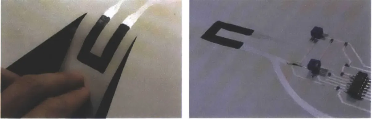
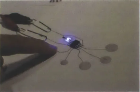
Touch Sensor
The touch sensor uses an ATTmy microcontroller and surface-mount LEDs to in-dicate output. As noted above, it uses loading-mode capacitive sensing. When it detects the touch of a finger on a painted capacitive pad, it lights an LED to indicate contact.
The implementation by which capacitance is detected on a single microcon-troller unit (MCU) pin is of some interest. To sense touch, the MCU rapidly cycles a pin between the input and output modes. In an AT'Iiny, setting a pin to input connects it to an internal pull-up resistor of about 20kQ. In setting the pin to OV and then pulling it high, a measurable amount of time elapses until the pin is read as high in the MCU's corresponding input port. Taking advantage of the Schmitt trigger on the input of each pin, the input toggles to high when the voltage on the pin has passed a certain threshold. The higher the capacitance on the pin, the longer it takes larger to charge, and the longer that read-time is. The time it takes to toggle is measured, and if it passes a certain threshold, a touch is signaled.
The touch sensor papercraft circuit, like the others, was constructed by painting a laser-cut mask designed in EAGLE and Adobe Illustrator. In Figure 4.12, the power is delivered through paper clips attached to conductive traces painted to the edge of the page.
Figure 4.11: Three-pad touch sensor with three Figure 4.12: Five-pad touch sensor with one
output LEDs. output LED.
Though, over time, elements of the silver ink appear to oxidize, the functionality remains unimpaired. Periodic recalibration made the sensing robust and able to
reliably detect touch in most situations. The designs here inform the choices made later, in the TinySynth study in Section 5.2.
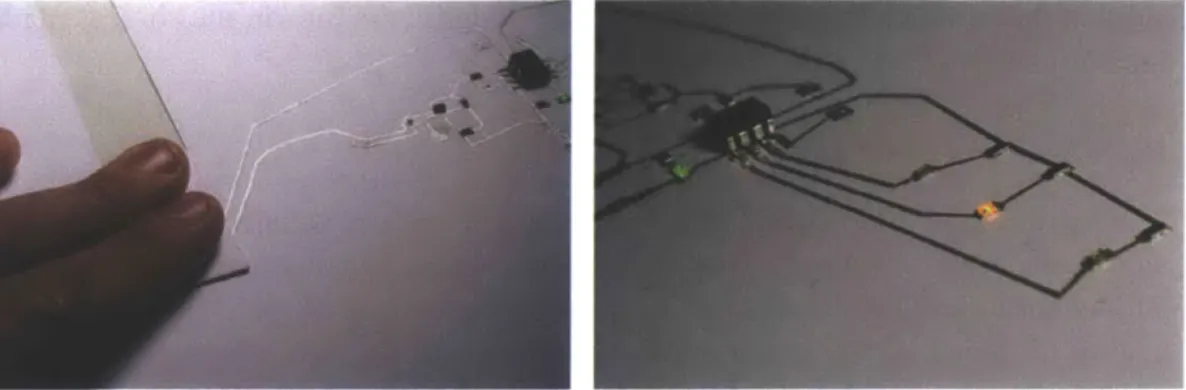
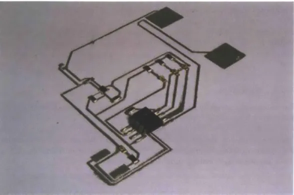
Force Sensor & Accelerometer
The force sensor and accelerometer (Figure 4.1) are adaptations of a similar de-sign, both using a transmit-receive capacitive sensor in conjunction with a tran-simpedance amplifier to generate a signal strong enough to be picked up by the analog-to-digital converter on an ATTiny45 microcontroller. An algorithm run-ning on the microcontroller samples the signal at appropriate intervals, capturing the signal induced on the receive electrode from the transmit electrode. As the two plates are brought together, the strength of the signal changes. The closer the two electrodes are, the stronger the current it induces on the receiving electrode. By synchronously under-sampling those changes at the appropriate time and smooth-ing the resultant signal, the relative position of the two electrodes can be tracked with some precision.
This basic configuration permits a variety of sensors to be constructed. Indeed, the only fundamental difference between the force sensor and the accelerometer is the configuration of the transmit-and-receive electrodes and the addition of a proof mass to the latter. In the final design, a series of surface-mount LEDs indicate the degree of pressure (or acceleration) as the sensor is actuated (Figure 4.16).
Figure 4.13: A folded paper "button" in an un- Figure 4.14: Full circuit, showing magnetic flexed state. "switch" to connect and disconnect power
leads.
While the technical aspects of the sensor are intriguing, the affordances offered
Figure 4.15: Pressing two electrodes together. Figure 4.16: The LEDs are light in proportion to the force exerted.
for paper and self-made devices. Because the device is created in a series of sequen-tial, accretive steps, its form, and correspondingly, its purpose, are fully mutable.
By cutting and folding the paper in different configurations, the nature of the
way in which the two electrodes sense their distance changes. Folding one electrode perpendicular with respect to other creates one sensing mode-folding in a different configuration creates another. The addition of a proof mass allows for the detection of changes in momentum perpendicular to the direction in which the fold is made. Once the principles of the sensors' operation are understand-sensing the distance between two electrodes-a spectra of possibilities present themselves. Conductive silver paint can be applied to both sides of an absorbent sheet of paper, and detect humidity as the sheet expands and contracts in width-or painted strips of tissue, hung in the wind, sensing the breeze moving through them. Of course, the envi-ronmental effects of moisture introduce other challenging envienvi-ronmental elements, corrupting
4.0.4 Reflection
There are two avenues of thought in considering paper-and-ink as a medium for cre-ating sensors. First, there are the technical and conceptual challenges of designing and making the devices themselves. These are the start-up costs, as simply assem-bling the necessary materials and designing the circuits themselves is challenging. It is a conventional challenge, though, and a familiar one. Once the original structure and the circuits are designed-in a way that derives more from conventional engi-neering than anything else-the process of making the sensors is novel. It consists
Figure 4.17: Capacitive plates at upper right, prior to cutting and folding. The circuit is not con-nected to power in this photo, which was supplied through the rectangular pads at lower left.
of a series of incremental, iterative steps, each adding a small feature or detail. The finished device gradually takes shape in a series of deliberate lines, cuts, and folds.
Each step brings an additional degree of refinement, and as it is repeated, con-tributes to a sense of a mastery and understanding of the device itself. Each succes-sive step is easier to complete once repeated. Applying conductive ink grows more familiar and less error-prone; the eye can evaluate with greater accuracy what con-nection is sound and what is not; when ink has slipped beneath a component and created a short; the glossy-sheen of wet-vs-dry. With growing skill comes growing confidence that each section is complete, and security that the device will function as expected. These are essential skills in the making of papercraft electronics, but orthogonal to those that are necessary for conventional electronics.
Creating sensors with the conductive ink also revealed some design patterns that would be repeated in later workshops. It is very difficult to salvage failed de-signs when working with the conductive ink. Smeared lines maintain some degree of conductivity and repeatedly modifying and tweaking fragile materials results in unwieldy, messy designs that were difficult to debug and verify. This motivated a
careful crafting process in which errors were strenuously avoided. That said, no sin-gle prototype took more than ten or fifteen minutes, all told, so though errors were devastating to a single piece-the corresponding costs of beginning again were low. Perhaps because I was making projects for the purposes of exploration, I generally found that I did not make more examples of a single piece once I had it working well.
4.0.5 Next steps
The process of creating paper sensors is challenging and difficult to share. Designing and cutting delicate masks requires the use of a laser cutter (or a very precise, patient hand) and the masking and subsequent weeding necessary can be time-consuming. In further exploring the generation of such papercraft devices, I will focus on re-ducing the overhead construction costs incurred in making such devices, paying particular attention to making enriching experiences for others.
Chapter
5
Microcontrollers meet Paper
This chapter examines two closely-related projects oriented around the Atmel AT-Tiny45/85 DIP microcontroller. This particular chip is ideal for papercraft elec-tronics because it is inexpensive and, with some additional hardware and software, easily-programmed from the Arduino environment (see Section 5.1.1). It is also rel-atively powerful and can easily handle most of the basic sensing and output needs that papercraft electronics might require. In mixing a microcontroller into the vo-cabulary of papercraft electronics, possibilities expand dramatically, creating av-enues for dual exploration: papercraft electronics can be explored both in its own right, as well as pathway to learn about and understand programming from the typically-challenging vantage of embedded devices.
5.1
Papercraft and Programming
In investigating papercraft electronics, there is a complimentary meeting of two seemingly-oppositional concepts. The first, is the manual, the tangible, the making of actual papercraft devices. Using scissors, glue, a careful eye and a steady hand, you can make remarkable electronics using only conductive ink, a few components, and a power source. Such devices, though, have a limit to their complexity. Only so much behavior can be teased out of a few lights. On the other hand, there is pro-gramming. The rich, infinitely-varied landscape of software adds a great deal to ways in which papercraft devices can be made. It also merges two kinds of making-the physical making of the tangible device, and the virtual programming of the micro-controller.
The purpose in this section is to begin to introduce the complexity of embed-ded programming into papercraft electronics. By mixing code into the slurry of materials and techniques that can be deployed in creating papercraft electronics, a panoply of possibilities emerge. In combining the craft of physical making with the craft of computer programming-the hope is that one will leach into the other, mu-tually reinforcing their strengths and augmenting their weaknesses. The potency of programming needs no explication; the relevancy of craft has been discussed pre-viously. The intention, in providing tools and materials for the creation of organic papercraft devices, is to cultivate a personal sense of understanding and ownership, derived from the making process.
In exploring these questions, we developed a suite of tools and techniques to ex-amine some of the consequences of combining programming with papercraft elec-tronics.
5.1.1 Our Materials
In introducing programming into the context of papercraft, we wanted to ensure that it was done in such a way that empowered participants to create. To that end, a set of complementary tools were developed to ease the process of programming small, embedded microcontrollers. The tools are open-source and were developed
by David Mellis building off of other open-source projects'.
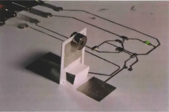
Our Tools
The TinyProgrammer (Figure 5.1) loads compiled programs onto an ATTiny45/85 DIP microcontroller, without any need for additional connections, wires, or com-ponents. The microcontroller slots directly into a socket on the programmer, which in turn, is plugged into the USB port of a computer. With the addition of the nec-essary board files-freely available online-the ATTiny45/85 can be programmed directly from the Arduino IDE. Most conventional Arduino-compatible commands work, with the exception of those that the ATTiny does not have the hardware to support. In addition to introducing the TinyProgrammer in the workshop, we also introduced the TinyUploader software.
TinyUploader (Figure 5.2) removes a step in the process of using the ATTiny, supplying a suite of pre-compiled programs that can be uploaded directly to the chip. This swaps one step in programming with another-the act of uploading code without actually seeing the code. The idea, here, was to demonstrate to participants
Figure 5.1: The TinyProgrammer board. Figure 5.2: A screenshot of the TinyUploader software with the precompiled 'touch' applica-tion selected.
that they had real agency over the functionality of embedded electronics, without introducing all of the overhead-complex syntax, logical flow constructs, etc.-that introducing coding incurs.
Materials
In addition to these auxiliary tools, participants were introduced to our suite of pa-percraft electronics materials: assorted paper, scissors, glue, conductive silver ink, and a variety of LEDs, as well as, the microcontrollers themselves.
5.1.2 Workshops
To test our techniques for papercraft electronics as well as our microcontroller tools, we conducted a workshop entitled "Papercraft and Programming." Through a series of guided activities, participants programmed and designed circuits on paper, pro-ducing a set of small, interactive projects. Surveys, as well as interrogative group-discussions, were conducted before and after the workshop to solicit feedback on participants' understanding and perceptions of the materials, as well as technology-production as a whole.
A dozen participants were recruited from the local community by way of flyers,
as well as from public email lists. Participants ages varied from 23 to 60. Ten of the twelve were women. All had attended at least some college, and seven had at least a bachelor's degree. Technical backgrounds varied considerably, with one participant working professionally as a computer programmer, and others never having seen a
Figure 5.3: Workshop materials and example
line of code. Among the group were a retiree, a teacher, an administrative assistant, and a chef.
After an initial discussion, participants were guided through the use of TmyPro-grammer and TinyUploader, uploading one of a small library of pre-compiled pro-grams. Each participant configured the required software and programmed an AT-Tiny for their own use. We then introduced squeeze bottles with conductive silver ink, as well as a simple paper template on which to affix a battery, the microcon-troller itself, and an LED. Workshop participants familiarized themselves with the basic principles of design with the materials, and completed a small circuit. We then introduced the Arduino IDE and the basics of embedded-systems C-programming with the Arduino libraries. After writing a small program, either from scratch or from included examples, participants constructed a papercraft project.
5.1.3 Artifacts
The final artifacts that participants constructed expressed a wide variety of inter-ests. One woman built a busy street-scene with blinking lights on paper cut-out
Figure 5.4: Papercraft and Programming
cars, another, a flickering campfire scene. One participant, drawing on her own art experience, drew a human figure with a blinking eye. Other projects were more util-itarian: a small, working lamp and an interactive greeting card. While some chose to use the conductive ink as a design element, others chose to hide it beneath lay-ers of paper. All projects were self-contained, incorporating a microcontroller, one or more LEDs, and battery. The microcontrollers were programmed with differ-ent behaviors, from simply fading or blinking various lights to responding to touch input.
5.1.4 Discussion
Over the course of the workshop, a number of central points of interest emerged. We focused on the accessibility and appeal of our techniques, the affordances of craft processes in making technology, making independent devices, and creating meaning through making.
Accessibility and appeal
Working with paper and conductive ink provides new avenues to engage people's interest. Some participants were intrigued by the papercraft from the beginning: "We were like, 'papercrafting, that sounds awesome ...let's go' I don't think we even read what it was about. But if you had started with 'Microcontroller Adjustment of
Paper Material' I would have been like I don't know what that means,' reported one participant.
Papercraft isn't just appealing to those specifically interested in the medium. The familiarity of working with paper and ink provided another avenue to comfort. One participant spoke about why she was interested: "I think for me, it wasn't even the papercraft, because I'm not really into papercrafting. But it was more that it seemed accessible. Papercraft is kind of like painting and drawing or writing. It seemed like it was easily transferable... It seemed like it wasn't terribly expensive, it seemed like it wasn't terribly out of reach for a regular person to do on their own."
The simplicity and versatility of the components also merited praise: "Great way to introduce [microcontrollers]. Easy to work with. Equipment wasn't so compli-cated." Another said: "It was a lot of fun. Really simple tools you can use to make almost anything, create almost anything. Almost everyone made something com-pletely different from paper, paint, and like two circuit elements."
Participants discussed the way that the language used to describe technology can influence the groups of people that are interested. One participant speculated that the workshop was specifically geared to appeal to groups typically excluded by the conventional language of electronics and technology design: "I was wondering, if with your title and your description.. .ifyou were trying to get more women involved or if you expected more women to be drawn to the craft aspect. Cause I generally think of craft as more feminine than more masculine. Whereas if it was microcon-trollers, I would think you would get more men than more women." Though the workshop was not explicitly targeted at any single group, it's noteworthy that the attendants were overwhelmingly female.
Affordances of a craft approach to technology
Integrating craft processes into the construction and design of technology intro-duces new skills and reframes the process of making technology as one of making craft. One participant commented: "The whole experience of working through and drawing the lines, you develop a sensitivity to where are they going to do and how are they working. They become part of the artwork or the craft." Workshop participants