HAL Id: hal-02543986
https://hal.archives-ouvertes.fr/hal-02543986
Submitted on 2 Jul 2020HAL is a multi-disciplinary open access archive for the deposit and dissemination of sci-entific research documents, whether they are pub-lished or not. The documents may come from teaching and research institutions in France or abroad, or from public or private research centers.
L’archive ouverte pluridisciplinaire HAL, est destinée au dépôt et à la diffusion de documents scientifiques de niveau recherche, publiés ou non, émanant des établissements d’enseignement et de recherche français ou étrangers, des laboratoires publics ou privés.
A nanoplatelet-based light emitting diode and its use for
all-nanocrystal LiFi-like communication
Junling Qu, Prachi Rastogi, Charlie Gréboval, Clément Livache, Marion
Dufour, Audrey Chu, Sang-Soo Chee, Julien Ramade, Xiang Zhen Xu,
Sandrine Ithurria, et al.
To cite this version:
Junling Qu, Prachi Rastogi, Charlie Gréboval, Clément Livache, Marion Dufour, et al.. A nanoplatelet-based light emitting diode and its use for all-nanocrystal LiFi-like communication. ACS Applied Materials & Interfaces, Washington, D.C. : American Chemical Society, 2020, �10.1021/ac-sami.0c05264�. �hal-02543986�
A nanoplatelet-based light emitting diode and its use for all-nanocrystal LiFi-like communication
Junling Qu1, Prachi Rastogi1, Charlie Gréboval1, Clément Livache1,2, Marion Dufour2, Audrey
Chu1, Sang-Soo Chee1, Julien Ramade1, Xiang Zhen Xu2, Sandrine Ithurria2, Emmanuel Lhuillier1* 1 Sorbonne Université, CNRS, Institut des NanoSciences de Paris, INSP, F-75005 Paris, France.
2 Laboratoire de Physique et d’Etude des Matériaux, ESPCI-Paris, PSL Research University,
Sorbonne Université Univ Paris 06, CNRS UMR 8213, 10 rue Vauquelin 75005 Paris, France.
Abstract: Since colloidal nanocrystals (NCs) were integrated as green and red sources for LCD
displays, the next challenge for quantum dots has been their use in electrically driven light emitting diodes (LEDs). Among various colloidal nanocrystals, nanoplatelets (NPLs) appeared as promising candidates for light emitting devices because their two-dimensional shape allows a narrow luminescence spectrum, directional emission and high light extraction. To reach high quantum efficiency it is critical to grow core/shell structures. High temperature growth of the shells seems to be a better strategy than previously reported low temperature approaches to obtain bright NPLs. Here, we synthesize CdSe/CdZnS core/shell NPLs whose shell alloy content is tuned to optimize the hole injection in the LED structure. The obtained LED has exceptionally low turn-on voltage, long-term stability (>3100 h at 100 Cd.m-2), external quantum efficiency above 5% and luminance
up to 35000 cd.m-2. We study the low-temperature performance of the LED and find that there is a
delay of droop in terms of current density as temperature decreases. In the last part of the paper, we design a large LED (56 mm2 emitting area) and test its potential for LiFi-like communication. In
such approach, the LED is not only a lightning source but also used to transmit a communication signal to a PbS quantum dot solar cell used as a broad band photodetector. Operating conditions compatible with both lighting and information transfer have been identified. This work paves the way toward an all nanocrystal-based communication setup.
Keywords: nanoplatelets, light emitting diode, efficiency droop, electronic transport,
nanocrystal-based communication
INTRODUCTION
Colloidal nanocrystals have been incorporated as green and red source into liquid crystal display (LCD), however, electrically pumped light emitting diodes (LEDs) application of them has been challenged.1 Even though there may remain several concerns (lifetime and light extraction) to reach
industrial integration, a key open question is related to the choice of the material. Among possible candidates, CdSe two-dimensional (2D) nanoplatelets (NPLs)2 appear as one of the most promising
because they combine (i) the narrowest photoluminescence (PL) signal,3 (ii) the high maturity of
II-VI nanocrystal colloidal syntheses, (iii) spectral tunability based on quantum confinement4–7 or doping8–11 with (iv) anisotropic emission diagram12, which means a macroscopic directive emission
can be obtained from a well-aligned NPLs assembly13,14, thus improving the light extraction
efficiency of LED devices by overcoming total internal reflection.
NPLs are 2D-shaped nanocrystals with confinement occurring only along the thickness. The specific growth mechanism of these nanocrystals leads to a lack of roughness along this direction and consequently the PL linewidth is not limited by inhomogeneous broadening as for spherical nanoparticles. Beyond their narrow luminescence spectrum, NPLs have also attracted interest for the design of transistors,15 light detectors16 and low threshold lasers.17–20 While the narrow PL
achieved by NPLs was enough to motivate the design of LED from core-only objects,6,21 the
integration of NPLs into LED has strongly benefit from the development of core/crown22 and
core/shell structures. For long, only low temperature methods,23 such as colloidal atomic layer
deposition,24 has been used for the growth of core/shell NPLs. This approach enhances the PL
efficiency by passivating surface dangling bonds and preserves the narrow linewidth of the NPLs, but the PL quantum efficiency remains generally limited below 50% with a large batch-to-batch fluctuation. In spite of these limitations, first core/shell NPL-based LEDs25,26 have been reported by
Chen et al.27 and improved latter by Giovanellaet al.28 More recently, high temperature growth of
shells on NPLs which preserve the 2D shape of the particles have been developed,29–35 leading to high PL efficiencies (90% and more) in the red. The improvement in the PL efficiency has significantly enhanced the electroluminescence (EL) efficiency34,36, which has brought the NPL
based LEDs to a new level of maturity and inspired the effort for their integration to more complex systems.
In this paper, we choose the strategy of integrating high temperature grown core/shell NPLs into LEDs. The shell alloy ratio is optimized to match the band alignment of the diode structure and favor the charge balance in the device. The obtained LED based on NPLs achieves 5.15% of external quantum efficiency (EQE), sub-bandgap turn-on voltage and shows an extrapolated half-lifetime of 3160 hours (time after which the emitted power drops by half for 100 Cd.m-2 luminance). We then
investigate transport in this LED at low temperature and show that the current droop occurs at higher current when temperature is decreased. We use this observation to suggest one path of improvement for this diode structure. Finally, we couple this LED to a NC-based solar cell used as a broad-band detector. We demonstrate that this couple of all NC-based devices can be used as a LiFi-like communication setup.
DISCUSSION
We start by growing core/shell NPLs made of a CdSe core and an alloyed shell of CdS and ZnS. Current NC-based LED structures rely on organic hole transport layers (HTLs) while electron transport layers (ETLs) are typically based on oxides (ZnO or TiO2). A successful structure for
CdSe-based nanocrystal LED has been proposed by Dai et al 37 which includes the following stack of
layers: ITO/PEDOT:PSS/Poly-TPD/PVK/NCs/ZnO/Ag, where PEDOT:PSS, Poly-TPD and PVK are respectively poly(3,4- ethylenedioxythiophene) polystyrene sulfonate, Poly(N,N'-bis-4-butylphenyl-N,N'-bisphenyl)benzidine and Poly(9-vinyl) carbazole. The HTLs have been identified as limiting blocks for the LED structure because of (i) the acidity of PEDOT:PSS which can etch the transparent conductive electrode, (ii) limited stability of the organic layer and (iii) lower carrier mobility of the HTLs with respect to ETL. To minimize the limitation coming from the HTL, we design the NPL in order to minimize the HTL/NPL energy barrier.
The highest occupied molecular orbital (HOMO) of the PVK is located 5.8±0.1 eV below the vacuum level. To determine the energy of the maximum of the valence band in the core/shell NPL, we use X-ray photoemission (XPS) and determine the work function (Figure 1c) and the relative position of the valence band with respect to the Fermi energy (Figure 1d). For ZnS shell, we found the valence band located 5.7±0.1 eV below the vacuum level, which is quasi resonant with the PVK within the accuracy of the photoemission.
To further optimize this band alignment and the balance of the charge injection, we tune the confinement energy. In NPLs changing the core level leads to discrete values for the band edge energy and this approach is not a continuous path to tune the band edge energy. Here we rather choose to tune the shell content thanks to alloying. The introduction of a small amount of CdS in the ZnS shell favor the electron delocalization over the whole structure, reducing the band edge energy. This allows a fine continuous tuning of the exact energy of the valence and conduction band. We observe that a 5% content of CdS within the CdZnS shell minimize the LED turns on voltage while maximizing its quantum efficiency, see figure S1 and table S1.
Figure 1 a. Absorption and photoluminescence spectra of CdSe/Cd0.05Zn0.95S core/shell
nanoplatelets. b. Transmission electron microscopy image of CdSe/Cd0.05Zn0.95S core/shell
nanoplatelets. c. Photoemission spectrum relative to the secondary electron cut-off for the core/shell nanoplatelets. d. Photoemission spectrum relative to the valence band for the core/shell nanoplatelets. e. Electronic spectrum of the core/shell nanoplatelets. f. Energy alignement for the LED. The energies for the different layers except the NPL are taken from ref. 27,37
We thus choose to focus on CdSe/Cd0.05Zn0.95S core/shell nanoplatelets in the following.30,38 The
absorption and PL of the material are given in Figure 1a. The PL peaks at 620 nm (≈2 eV) and presents a full width at half maximum (FWHM) of 27 nm. The particles are of a parallelipedic shape with a lateral extension of 10x40 nm2 as shown on Figure 1b. Photoemission spectra unveil a work
function of 4.4 eV and a Fermi level deep in the band gap located 1.3 eV above the valance band. This suggests a n-type nature for this material, consistent with previous transport measurements for
CdSe core based NPLs.15 We thus propose an effective electronic spectrum for the heterostructure
as given in Figure 1e. The chosen alloy composition provides a quasi-resonant band alignment with the HTL, while reducing the band conduction band offset with ZnO compared to pure ZnS shell, see Figure 1f.
We build the all solution-processed ITO/PEDOT:PSS/Poly-TPD/PVK/NCs/ZnO/Ag diode with the optimized NCs layer, see a scheme of the device in Figure 2a. We also add an encapsulation layer to avoid any exposure of the device to oxygen and moisture during operation. In the following, the device is stored and operated in room condition (i.e. air exposed). The LED presents an EL spectrum which matches the band gap of CdSe/Cd0.05Zn0.95S core/shell nanoplatelets, with an peak
wavelength at 622 nm, see Figure 2b. The FWHM of the EL is 28 nm. The CIE coordinate in the chromaticity diagram is shown in Figure 2c. Note that the emission of the NPL based LED follows a Lambertian angular dependence, see Figure S2.
Figure 2 a. Scheme of the LED made of glass/ITO/hole transport layers (PEDOT :PSS/PolyTPD/PVK)/ CdSe/Cd0.05Zn0.95S core/shell nanoplatelets/ZnO/Ag. b.
Electroluminescence spectra of the LED which emitting layer is made of CdSe/Cd0.05Zn0.95S
core/shell nanoplatelets at room temperature and under various applied bias. c. Chromaticity diagram and the color associated with the spectrum of the LED based on CdSe/Cd0.05Zn0.95S
core/shell nanoplatelets.
The I-V curve, luminance and EQE of the device are then shown in Figure 3a and b. The diode presents a sub-bandgap threshold with a turn on voltage as low as 1.63 V (about 0.4 V lower than the band gap), which is the lowest reported so far.39 The maximum EQE has been determined to
be 5.15%, partly limited by the PL efficiency of around 35%. The luminance can reach 35 100 cd.m -2 under 7 V operation, see Figure S3. The lifetime of the diode with an initial luminance of 73 cd.m -2 and 1000 cd.m-2 have been monitored, under constant current. A reasonable extrapolation allows
to estimate that 50% of the extracted power will remain after 11 000 h (at 73 cd.m-2), see Figure 3c.
Under higher luminance of 1000 cd.m-2, we found the half lifetime to be 100 h, see figure S4.
Assuming that the L1.5T
50 is constant37, with L the initial luminance and T50 the duration when the
LED drops to half of its efficiency, we can determine the half lifetime under 100 cd.m-2 luminance to
beat least 3160 h.
It is worth pointing that Kelestemur et al34 recently reported a similar LED based on core/shell NPLs
grown at high temperature and for which the HTL is made of PEDOT:PSS and PVK. Our LED achieve better EQE than the CdSe/CdS NPL-based LED but lower than the one based on core/shell/shell (CdSe/CdS/CdZnS) NPL. The latter material leads to EQE as high as 10%, but the
turn-on voltage (2.3 V) is higher. It indicates a less optimized band alignment for charge injection. More comparisons of the LED performance with previously reported LED based on NPLs are given in Table 1.
Figure 3 .a Current density and luminance as a function of the applied bias for the LED based on CdSe/Cd0.05Zn0.95S core/shell nanoplatelets. b. External quantum efficiency (EQE) and luminance
as a function of the driving current. c. Normalized light power extracted from the LED as a function of time. The LED is driven under a constant current of 14 µA here which correspond to a initial luminance of 73 cd.m-2. The experimental data are in black, while the red(solid) curve is an
extrapolation. The extracted power drops by half after ≈11 000 h.
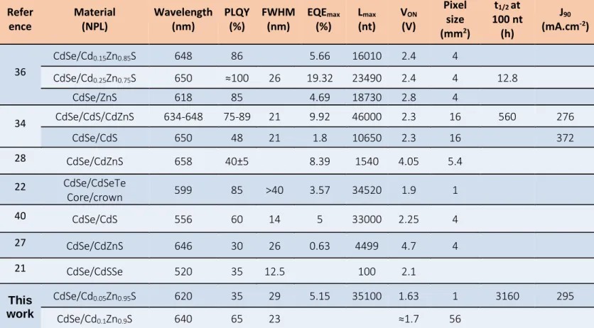
Table 1 : Comparison of different figure of merit for NPL-based LEDs
Refer ence Material (NPL) Wavelength (nm) PLQY (%) FWHM (nm) EQEmax (%) Lmax (nt) VON (V) Pixel size (mm2) t1/2 at 100 nt (h) J90 (mA.cm-2) 36 CdSe/Cd0.15Zn0.85S 648 86 5.66 16010 2.4 4 CdSe/Cd0.25Zn0.75S 650 ≈100 26 19.32 23490 2.4 4 12.8 CdSe/ZnS 618 85 4.69 18730 2.8 4 34 CdSe/CdS/CdZnS 634-648 75-89 21 9.92 46000 2.3 16 560 276 CdSe/CdS 650 48 21 1.8 10650 2.3 16 372 28 CdSe/CdZnS 658 40±5 8.39 1540 4.05 5.4 22 CdSe/CdSeTe Core/crown 599 85 >40 3.57 34520 1.9 1 40 CdSe/CdS 556 60 14 5 33000 2.25 4 27 CdSe/CdZnS 646 30 26 0.63 4499 4.7 4 21 CdSe/CdSSe 520 35 12.5 100 2.1 This work CdSe/Cd0.05Zn0.95S 620 35 29 5.15 35100 1.63 1 3160 295 CdSe/Cd0.1Zn0.9S 640 65 23 ≈1.7 56
The LED shows interesting performance such as a narrow EL signal, low turn-on operation and long lifetime, however, under high driving current, we observe an efficiency droop. Efficiency droop is a
general feature for LEDs and nanocrystal-LEDs where the EQE decreases with the higher current. Currently, the most common strategy to prevent the efficiency droop is to design the nanocrystal band profile to reduce the Auger effect.41 Graded interfaces has been proposed as a possible route
to reach this goal.42
We then investigate the thermal properties of the LED, because low temperature transport is a powerful probe to reveal transport mechanisms and possible ways to improve LED structure. Upon cooling the EL signal shows a blue shift which follows the shift of the PL signal. Thus, we can attribute the EL shift to the change of band gap of NPLs with temperature. Temperature- dependent transport reveals two regimes of bias in the I-V curve. In the first region at low bias, typically below the turn-on voltage of the LED, the transport is almost temperature independent, see Figure 4a and S2. At higher bias, the current depends more strongly on the temperature and we particularly observe a shift of the voltage (Vt) where the device enters a strongly conductive state. This shift is
also responsible for a similar shift of the turn-on voltage with temperature in the EQE curve as a function of bias, see Figure 4c. We may have naively attributed this shift of the transport and EQE to the change of band gap with temperature. However, the shift of PL and EL with temperature are much smaller than the one observed in transport, see Figure S5 and S6. Indeed, this shift with temperature in the I-V curve is also observed in the diode built without NPLs, see Figure S7. As a result, we believe that the NPLs are not related to the shift. This is consistent with the situation where in NC-LEDs the nanoparticles are mostly a recombination center and transport is entirely driven by the ETL and HTLs. Complementarily with the shift of the turn-on voltage depending on the temperature, we observe that the EQE droop is shifted toward higher current density at lower Figure 4d and its inset.
The fact that the appearing of the droop is strongly temperature-dependent suggests two origins for the droops. The first path is the temperature-dependent Auger recombination within the NPL43,44.
Temperature dependence of the Auger process remains so far uninvestigated in NPL. However, NPLs thanks to their large volume45 should present a reduced auger recombination with respect to
other kinds of nanocrystals. In addition, NPL with thin shell, as it is here, are supposed to be the one with the lowest Auger rate46. Thus, it is likely that the delay of droop is assisted by Auger effect
occurring in the transport layers. Such speculation is supported by the fact that the shift of the Vt, which follows shift of the droops with temperature, is also observed in the NPL free device, see Figure S7.
Figure 4 a. Current as a function of bias under various temperatures of the LED based on CdSe/Cd0.05Zn0.95S core/shell nanoplatelets. b. Electroluminescence spectra obtained at different
temperatures under 5 V bias. A clear red-shift is observed as the temperature increases. c. Uncalibrated EQE as a function of the applied bias for various temperatures . d. Uncalibrated EQE as a function of the driving current under different temperatures.
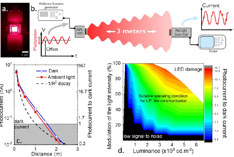
Nanocrystals-based LEDs and detectors have for the moment been used independently. The maturity of these devices has reached a high level, which motivates their integration into more complex systems. Here, we explore the possibility to design an all-nanocrystal-based communication setup which operates in LiFi-like operation. In such setup, a light source, here the NPL-based LED, is used not only for lightning but also to send information. For this application, we have updated the LED device and expanded it to a larger active area, typically 7x8 mm2 to generate
more photons, see Figure 5a. The thicknesses of the ZnO and PEDOT:PSS layers have also been increased to prevent electrical shorts in the device which are more likely to occur as the device size is increased. However, the device structure maintained and so is the low turn-on voltage around 1.7 V. The electrical and optical characteristics of the diode are given in Figure S8 and S9.
As a sensor, we use a PbS nanocrystal-based solar cell which have been proved to be an efficient broad band absorber over the visible range. We fabricate solar cell structure proposed by Chuang et al47 and the detailed fabrication can be found in the supporting information and ref48. The PbS
solar cell characteristics are given in Figure S10. Briefly, the structure relies on PbS nanocrystals with a band gap at 920 nm. The n junction is made of a thick layer of iodide-capped PbS and a p-type layer of ethanedithiol capped PbS nanocrystals. The dark current of such diode operated at 0 V can be as low as 10 nA.cm-2 and the diode present a strong current modulation under illumination.
Interestingly, the time response of the diode has been found to be 10 ns for the rise time and 1 µs for the decay time. This is too slow to establish a high speed (GHz or THz) telecommunication channel but can be used to transfer information. To operate this system, we apply a constant driving voltage to the LED, which is compatible with lightning application. On the top of this signal we set-up an AC modulated (@10kHz here) signal to generate signal modulation. The light is then collected by the solar cell as described in Figure 5b. The current in the photodiode is then filtered to keep the AC part only.
Figure 5 a. Picture of the large LED based on NPLs under operation. b. Scheme of the developed communication setup. The LED is driven with a constant bias on the top of which a modulated signal is applied. The signal is then collected on a PbS nanocrystal based solar cell used as broad band detector. The AC component of the signal is then amplified using a lock-in setup. c. Photocurrent and photocurrent to dark current ratio as a function of the LED to detector distance. 1 /R2 decay law
is also plotted. Signal is modulated at 10 kHz here. d. Photocurrent to dark current ratio as a function of the luminance of the LED and as a function of the signal modulation. 100% modulation means that the LED is turned on and off, while for lower modulation the LED is always emitting some light.
We first investigate how the distance between the source and the detector affects the signal acquisition, see Figure 5c. In the current configuration, where signal collection is not optimized and conservative bias are applied on the LED, photocurrent to dark current ratio above 1 can be preserved up to 1.5 m. The drop of the signal with distance follows a decay slower than 1/R2 (ie the
optical power decay), with R the source to detector distance. We attribute this behavior to the improvement in the quantum efficiency of the solar cell when the incident power flux is reduced. We also consider the impact of the luminance and the signal modulation amplitude of the LED, see Figure 5d. For luminance compatible with lightning (5000 cd.m-2), we can conserve photocurrent to
dark current ratio above 1 for signal modulation as low as 25% which is not eye detectable. Transmission of binary signal, beyond a simple plane wave, has also been tested with a 1 m distance, see Figure S11 and the obtained signal matches the LED input.
CONCLUSION
We build a LED based on core/shell NPLs grown at high temperature. The obtained diode presents a maximal EQE of 5.15% with a record low turn-on voltage of 1.63 V and extremely long lifetime (3160 h at 100 cd.m-2). Under large current injection an efficiency droop appears, where the current
threshold of droop appears to be strongly temperature dependent. Lower temperatures shift the droop toward larger current density. Such strong temperature dependence on the droop threshold suggest that future efforts need to be focused on the transport layers. We have also successfully demonstrated the potential of the LED into a LiFi-like communication setup and show that communication can be obtained once the LED is coupled to a solar cell as a detector. This paves the way for future developments of all nanocrystal-based communication setup.
METHODS
Chemicals for NPL growth : Octadecene (ODE, Alfa Aeser, 90%), cadmium acetate dihydrate
(Cd(Ac)2, Sigma, 98%), cadmium oxide (CdO, Strem, 99.99%), zinc oxide (ZnO, Sigma, 99,99%),
myristic acid (Fluka, 98%), oleic acid (OA, Alfa Aesar, 90%), selenium powder (Strem Chemicals 99.99%), zinc acetate dihydrate (Aldrich, 98%), octanethiol (Fluka, 97%), Trioctylamine (TOA, sigma aldrich, 98%), hexane (VWR, 99%), ethanol (EtOH, VWR, < 99%), toluene (Carlo Erba, < 99%), methanol (VWR, < 99%).
Precursors:
Cadmium myristate Cd(Myr)2: In a 50 mL three neck flask, 2.56 g of CdO and 11 g of myristic acid
were mixed and degassed at 90 °C for an hour. Then, under Ar flux, the temperature was set to be 200 °C. When the solution turns colorless (in approximately 40 minutes), the reaction was stopped and the temperature decreased. At 60 °C, 30 mL of methanol were added to the mixture. The cadmium myristate was washed 4 times with methanol and dried overnight at 50 °C under vacuum.
Cadmium oleate in ODE (0.1M): CdO (6.42 g, 50 mmol) was added to 100 mL of OA in a 250 mL
three-neck flask and heated at 160 °C. When the mixture became colorless, the flask is cooled down to 70 °C and degassed under vacuum for 1 h. Then 400 mL of ODE were added to obtain the final concentration. The solution was transferred into a bottle and stored for several months. The precursor was heated prior to use.
Zinc oleate in ODE (0.1 M): In a 250 mL flask, 50 mmol of ZnO (4.074 g) and 100 mL of OA are
introduced. The mixture was heated to 180 °C and stayed at that temperature until there was a clear solution. The reaction was cooled down immediately to 120 °C and degassed at this temperature to remove the water. Then the heating mantle was removed, and the mixture were allowed to cool down naturally. To get 0.1 M zinc oleate, 16 mL of ODE was added to 4 mL of 0.5 M zinc oleate. The precursor was heated prior to use.
CdxZn1-x oleate (0.1 M) can be obtained by mixing cadmium oleate (0.1 M) and zinc oleate (0.1 M)
described above according to the desired ratio.
CdSe core nanoplatelets synthesis: A mixture of 340 mg of Cd(Myr)2 (0.6 mmol), 24 mg of Se powder (0.3 mmol) and 30 mL of ODE were degassed in a three neck flask for 30 min under vacuum. Then, under Ar flux, the temperature was set to 240 °C and as it reached 180 °C, 80 mg (0.3 mmol) of Cd(OAc)2•2H2O solid was rapidly added to the flask. 12 min after the addition of Cd(OAc)2, the
reaction was quenched by injecting 2 mL of OA . Then the mixture was cooled down to room temperature. Hexane and ethanol were added to the reaction mixture before it was precipitated by centrifugation. A second cleaning was conducted with hexane/ethanol and the final CdSe core nanoplatelets were redispersed in 12 mL of ODE.
CdSe/CdxZn1-xS core/shell nanoplatelets synthesis: The recipe was taken from literature with
modifications.30 15 mL of TOA was added to a 100 mL three-neck flask and degas at 100 °C for 30
min. Then the atmosphere was switched to Ar and the temperature was set to 300 °C. Meanwhile, 7 mL of 0.12 M octanethiol and 7 mL of 0.1 M of CdxZn1-x oleate (x=0.05 or 0.1) were put into two
syringes and set on a pump. When the temperature stabilized at 300 °C, the syringe pump was started and pumped at a constant rate of 4.7 mL/h. After several drops of pumping, 3 mL of NPL core in ODE were swiftly injected to the flask. Then the mixture was baked for another 90 min at 300 °C after all the injection were finished. The flask was then cooled down with air flux and at the temperature of 100 °C, 2 mL of OA was injected. 15 mL of hexane and 10 mL of ethanol were added to precipitate the NPLs by centrifugation. After a second purification with ethanol and hexane, the NPLs were finally dispersed in 5 mL of toluene.
Material characterization
Absorption and photoluminescence: JASCO V-730 spectrometer was used for UV-Visible
spectroscopy. Photoluminescence (PL) spectra and PL quantum yield in a solution sample were obtained by an Edinburgh Instrument spectrometer.
Transmission electron microscopy image: A JEOL 2010 transmission electron microscope
operated at 200 kV was used to observe the nanocrystals. The grids were prepared by drop casting a diluted solution of NPLs dispersed in toluene and degassed overnight under secondary vacuum to remove left over of solvent and volatile organics.
X-ray photoemission measurements (XPS): For ultraviolet photoemission spectroscopy, the films
of nanocrystals were spin-casted on a gold coated Si substrate (gold layer is 80 nm thick). The film was ligand exchanged by dipping the film into a 1% in volume solution of ethanedithiol in ethanol. The samples were introduced in the preparation chamber and degassed until the vacuum reached
below 10-9 mbar. Then samples were introduced to the analysis chamber. Photo energy in the 60 to
1000 eV range were used. The signal was acquired by a detector SCIENTA SES2002 analyzer equipped with a delay line detector developed by ELETTRA. A gold substrate was used to measure the Fermi energy. The exact value of the energy of the beamline was determined by measuring the second harmonic of Cd core level peaks. The measurement of the low binding part of the photoemission spectrum was used to determine the value of VB-EF. Then the energy of the
conduction band was determined from the valence band offset by the absorption gap. Finally, the work function was determined by measuring the cut-off of secondary electrons.
LED fabrication
Materials for LED: PEDOT:PSS (poly(3,4- ethylenedioxythiophene) polystyrene sulfonate, Al 4083,
M121, Ossila), Poly-TPD (Poly(N,N'-bis-4- butylphenyl-N,N'-bisphenyl)benzidine, Ossila), PVK (Poly(9-vinyl) carbazole, average Mn 25,000-50,000, Aldrich), Chlorobenzene (anhydrous, 99.8%, Sigma-Aldrich), m-Xylene (anhydrous, ≥99%, Sigma-Aldrich), Zinc acetate dihydrate (97+%, Alfa Aesar), Tetramethylammonium hydroxide pentahydrate (TMAOH, 98%, Alfa Aesar), Dimethyl Sulfoxide (DMSO, ≥99.9%, Sigma-Aldrich), ethyl acetate (VMR), ethanol absolute anhydrous (VMR), acetone (VWR), and toluene (Carlo Erba, 99.3%). All the materials were used as received.
Synthesis of ZnO nanoparticles: The procedure was taken from ref 37. In flask A, 3 mmol of Zinc
acetate were dissolved in 30 mL of DMSO by vigorous stirring. At the same time, 5.5 mmol of TMAOH were dissolved with 10 mL of ethanol in flask B. Then the content of the two flasks were mixed and stirred for 24 hours under ambient conditions. The reaction mixture turned whitish during the first few seconds and became clear soon after. ZnO particles were precipitated by ethyl acetate and redispersed in ethanol. 160 µL of 2-ethanolamine were added to stabilize the nanoparticles before they were precipitated and redispersed with ethyl acetate and ethanol respectively again. Finally, the ZnO nanoparticles in ethanol is filtered using a 0.22 µm PTFE filter.
ITO substrate patterning: ITO substrates (10 Ω/sq) were cut into 15 mm × 15 mm pieces and
cleaned by sonication in acetone for 5 min. After sonication, the substrates were rinsed with acetone and isopropanol before dried completely with N2 flow. The substrates were further cleaned with O2
plasma for 5 min to remove organic residuals on the surface. After cleaning, TI-Prime and AZ 5214E photoresist were sequentially spin-coated on the surface of ITO substrates at the rate of 4000 rpm for 30 s and baked at 110 °C for 120 s and 90 s, respectively. In the next stage, a mask aligner was used to expose the substrates to UV light for 20 s through a lithography mask (1 mm width). Photoresist was then developed using AZ 726 developer for 20 s before rinsed with deionized water and dried with N2 flux. After another 5-minute plasma cleaning, the substrates were etched in a 25%
HCl (in water) bath for 10 min at 40 °C before they were dipped immediately in deionized water. Finally, the lift-off was conducted in an acetone bath. Before using, the patterned ITO substrates were cleaned with acetone and isopropanol first and put under plasma for 10 min.
LED Fabrication: PEDOT:PSS solution (filtered through 0.45 µm filter) was spin-coated on a
patterned ITO glass electrode at 4000 rpm for 60 s and annealed at 140 °C for 10 min in air. Inside a Nitrogen-filled glovebox, Poly-TPD (8 mg.mL-1 in chlorobenzene), PVK (1.5 mg.mL-1 in m-xylene),
NPLs and ZnO nanoparticles were successively spin-coated at 2000 rpm for 45 s on the PEDOT: PSS-coated substrate. After the deposition of Poly-TPD, the sample was annealed at 110 °C for 20 min, and for PVK the annealing was at 170 °C for 30 min. Finally, 80 nm of Ag was deposited on top of the ZnO using a shadow mask by thermal evaporation. The thickness of NPL and ZnO layer were 18 nm and 80 nm respectively, as obtained by profilometry. The devices were encapsulated
inside the glove box with a piece of glass by Araldite crystal glue. The size of the pixel was 1 mm2
which was the overlap of ITO and Ag electrode.
LED characterization:
The EQE of the device was determined according to the method from Ref49. Considering the
Lambertian emission of LED device, the flux leaving the device directly can be described as 𝐹𝑒𝑥𝑡 = ∫ 2𝜋𝐿0
π/2
0 𝑐𝑜𝑠𝜃 𝑠𝑖𝑛𝜃 𝑑𝜃 = 𝜋𝐿0, with 𝐿0 the flux per solid angle of light leaving the device in the
forward direction. Since the solid angle from the photodetector to the light source is Ω =𝑆1
𝑙2 with 𝑆1
the area of the detector and 𝑙 the distance between the light source and detector, then 𝐿0 = 𝑃𝑑𝑒𝑡 Ω = 𝑃ⅆ𝑒𝑡𝑙2
𝑠1 and 𝐹𝑒𝑥𝑡 =
𝜋𝑃ⅆ𝑒𝑡𝑙2
𝑠1 . The number of photons emitted per second to the forward direction then
can be calculated by 𝑁𝑃 = 𝐹𝑒𝑥𝑡
ℎ𝜈 =
𝜋𝑃ⅆ𝑒𝑡𝑙2𝜆
𝑠1ℎ𝑐 , with 𝜆 the wavelength of electroluminescence, ℎ the
Plank’s constant and 𝑐 the speed of light. The number of electrons injected per second can be obtained by 𝑁𝑃 = 𝐼
𝑒, with 𝐼 the current flow of the device. Thus, the EQE can be calculated as 𝐸𝑄𝐸 = 𝑁𝑝
𝑁𝑒 =
𝜋𝑃ⅆ𝑒𝑡𝑙2𝜆𝑒
𝑠1ℎ𝑐𝐼 . The irradiance of the device is 𝑅 = 𝐹𝑒𝑥𝑡
𝑠2 =
𝜋𝑃ⅆ𝑒𝑡𝑙2
𝑠1𝑠2 , with 𝑆2 the area of the pixel. The
luminance of the device 𝐿 =683.𝑉(𝜆).𝐹𝑒𝑥𝑡
𝜋.𝑆2 , with 𝑉(𝜆) the function of photonic eye sensitivity. For the
characterization, we collected current-voltage-luminance characteristics with a Keithley K2634B sourcemeter unit and a PM100A powermeter coupled with the S120C Si detector from Thorlabs. Knowing that the working diameter of detector area is 9.5 mm and assuming the distance between detector and device to be 6.5 mm, the geometry related value of 𝑙
2
𝑠1 ≈ 0.6.
Operation of the communication setup:
To probe the ability of the LED for all-nanocrystal-based communication we used a MFLI lock-in amplifier to drive the LED and measure the detected signal from the PbS solar cell. The signal output of the MFLI was used to send a periodic signal composed of an offset voltage (Voffset) over which is
added a sinusoidal signal at 10 kHz with an amplitude (zero-to-peak) of Vpk. On the detection side,
the solar cell is operated at 0 V bias and current is amplified through a Femto DLPCA-100 transimpedance amplifier (TIA). The output voltage of the TIA was then sent to the signal input of the lock-in. After demodulation the photocurrent at the reference frequency is measured. The amplitude of the modulation is defined as 𝑉pk/𝑉offset.
ACKNOWLEDEGMENTS
The project is supported by ERC starting grant blackQD (grant n° 756225) and Ne2Dem (grant n° 853049). We acknowledge the use of clean-room facilities from the “Centrale de Proximité Paris-Centre”. This work has been supported by the Region Ile-de-France in the framework of DIM Nano-K (grant dopQD). This work was supported by French state funds managed by the ANR within the Investissements d'Avenir programme under reference ANR-11-IDEX-0004-02, and more specifically
within the framework of the Cluster of Excellence MATISSE and also by the grant IPER-Nano2, Copin, Frontal, Graskop. JQ thanks Chinese Scholarship Council for PhD grant while AC thanks Agence innovation defense.
Additional information
Supplementary information is available for this paper at. It includes informations relative to the LED characterization (angular dependence operation under high electric field, low temperature operation), Operation of the all nanocrystal-based communication setup (large scale LED fabrication, solar cell fabrication and characterization, transmission of binary signal). A video illustrating the operation of the LEDs under pulsed mode is also provided.
REFERENCES
(1) Wood, V.; Bulović, V. Colloidal Quantum Dot Light-Emitting Devices. Nano Reviews 2010, 1, 5202. (2) Lhuillier, E.; Pedetti, S.; Ithurria, S.; Nadal, B.; Heuclin, H.; Dubertret, B. Two-Dimensional Colloidal
Metal Chalcogenides Semiconductors: Synthesis, Spectroscopy, and Applications. Acc. Chem. Res. 2015, 48, 22–30.
(3) Tessier, M. D.; Javaux, C.; Maksimovic, I.; Loriette, V.; Dubertret, B. Spectroscopy of Single CdSe Nanoplatelets. ACS Nano 2012, 6, 6751–6758.
(4) Christodoulou, S.; Climente, J. I.; Planelles, J.; Brescia, R.; Prato, M.; Martín-García, B.; Khan, A. H.; Moreels, I. Chloride-Induced Thickness Control in CdSe Nanoplatelets. Nano Lett. 2018, 18, 6248– 6254.
(5) Diroll, B. T.; Schaller, R. D. Shape-Selective Optical Transformations of CdSe Nanoplatelets Driven by Halide Ion Ligand Exchange. Chem. Mater. 2019, 31, 3556–3563.
(6) Dufour, M.; Qu, J.; Greboval, C.; Méthivier, C.; Lhuillier, E.; Ithurria, S. Halide Ligands To Release Strain in Cadmium Chalcogenide Nanoplatelets and Achieve High Brightness. ACS Nano 2019, 13, 5326–5334.
(7) Cho, W.; Kim, S.; Coropceanu, I.; Srivastava, V.; Diroll, B. T.; Hazarika, A.; Fedin, I.; Galli, G.; Schaller, R. D.; Talapin, D. V. Direct Synthesis of Six-Monolayer (1.9 Nm) Thick Zinc-Blende CdSe Nanoplatelets Emitting at 585 Nm. Chem. Mater. 2018, 30, 6957–6960.
(8) Khan, A. H.; Pinchetti, V.; Tanghe, I.; Dang, Z.; Martín-García, B.; Hens, Z.; Van Thourhout, D.; Geiregat, P.; Brovelli, S.; Moreels, I. Tunable and Efficient Red to Near-Infrared Photoluminescence by Synergistic Exploitation of Core and Surface Silver Doping of CdSe Nanoplatelets. Chem. Mater. 2019, 31, 1450–1459.
(9) Sharma, M.; Olutas, M.; Yeltik, A.; Kelestemur, Y.; Sharma, A.; Delikanli, S.; Guzelturk, B.; Gungor, K.; McBride, J. R.; Demir, H. V. Understanding the Journey of Dopant Copper Ions in Atomically Flat Colloidal Nanocrystals of CdSe Nanoplatelets Using Partial Cation Exchange Reactions. Chem. Mater. 2018, 30, 3265–3275.
(10) Dufour, M.; Izquierdo, E.; Livache, C.; Martinez, B.; Silly, M. G.; Pons, T.; Lhuillier, E.; Delerue, C.; Ithurria, S. Doping as a Strategy to Tune Color of 2D Colloidal Nanoplatelets. ACS Appl. Mater. Interfaces 2019, 11, 10128–10134.
(11) Liu, B.; Sharma, M.; Yu, J.; Shendre, S.; Hettiarachchi, C.; Sharma, A.; Yeltik, A.; Wang, L.; Sun, H.; Dang, C.; et al. Light-Emitting Diodes with Cu-Doped Colloidal Quantum Wells: From Ultrapure Green, Tunable Dual-Emission to White Light. Small 2019, 15, 1901983.
(12) Feng, F.; Nguyen, L. T.; Nasilowski, M.; Nadal, B.; Dubertret, B.; Coolen, L.; Maître, A. Consequence of Shape Elongation on Emission Asymmetry for Colloidal CdSe/CdS Nanoplatelets. Nano Res. 2018, 11, 3593–3602.
(13) Jana, S.; Phan, T. N. T.; Bouet, C.; Tessier, M. D.; Davidson, P.; Dubertret, B.; Abécassis, B. Stacking and Colloidal Stability of CdSe Nanoplatelets. Langmuir 2015, 31, 10532–10539.
(14) Yoon, D.-E.; Kim, W. D.; Kim, D.; Lee, D.; Koh, S.; Bae, W. K.; Lee, D. C. Origin of Shape-Dependent Fluorescence Polarization from CdSe Nanoplatelets. J. Phys. Chem. C 2017, 121, 24837–24844. (15) Lhuillier, E.; Ithurria, S.; Descamps-Mandine, A.; Douillard, T.; Castaing, R.; Xu, X. Z.; Taberna, P.-L.;
Simon, P.; Aubin, H.; Dubertret, B. Investigating the N- and p-Type Electrolytic Charging of Colloidal Nanoplatelets. J. Phys. Chem. C 2015, 119, 21795–21799.
(16) Lhuillier, E.; Robin, A.; Ithurria, S.; Aubin, H.; Dubertret, B. Electrolyte-Gated Colloidal Nanoplatelets-Based Phototransistor and Its Use for Bicolor Detection. Nano Lett. 2014, 14, 2715–2719.
(17) She, C.; Fedin, I.; Dolzhnikov, D. S.; Dahlberg, P. D.; Engel, G. S.; Schaller, R. D.; Talapin, D. V. Red, Yellow, Green, and Blue Amplified Spontaneous Emission and Lasing Using Colloidal CdSe Nanoplatelets. ACS Nano 2015, 9, 9475–9485.
(18) Grim, J. Q.; Christodoulou, S.; Di Stasio, F.; Krahne, R.; Cingolani, R.; Manna, L.; Moreels, I. Continuous-Wave Biexciton Lasing at Room Temperature Using Solution-Processed Quantum Wells. Nature Nanotechnology 2014, 9, 891–895.
(19) Rossinelli, A. A.; Rojo, H.; Mule, A. S.; Aellen, M.; Cocina, A.; De Leo, E.; Schäublin, R.; Norris, D. J. Compositional Grading for Efficient and Narrowband Emission in CdSe-Based Core/Shell Nanoplatelets. Chem. Mater. 2019, 31, 9567–9578.
(20) Olutas, M.; Guzelturk, B.; Kelestemur, Y.; Yeltik, A.; Delikanli, S.; Demir, H. V. Lateral Size-Dependent Spontaneous and Stimulated Emission Properties in Colloidal CdSe Nanoplatelets. ACS Nano 2015, 9, 5041–5050.
(21) Fan, F.; Kanjanaboos, P.; Saravanapavanantham, M.; Beauregard, E.; Ingram, G.; Yassitepe, E.; Adachi, M. M.; Voznyy, O.; Johnston, A. K.; Walters, G.; et al. Colloidal CdSe1–XSx Nanoplatelets with Narrow and Continuously-Tunable Electroluminescence. Nano Lett. 2015, 15, 4611–4615. (22) Liu, B.; Delikanli, S.; Gao, Y.; Dede, D.; Gungor, K.; Demir, H. V. Nanocrystal Light-Emitting Diodes
Based on Type II Nanoplatelets. Nano Energy 2018, 47, 115–122.
(23) Mahler, B.; Nadal, B.; Bouet, C.; Patriarche, G.; Dubertret, B. Core/Shell Colloidal Semiconductor Nanoplatelets. J. Am. Chem. Soc. 2012, 134, 18591–18598.
(24) Ithurria, S.; Talapin, D. V. Colloidal Atomic Layer Deposition (c-ALD) Using Self-Limiting Reactions at Nanocrystal Surface Coupled to Phase Transfer between Polar and Nonpolar Media. J. Am. Chem. Soc. 2012, 134, 18585–18590.
(25) Xiao, P.; Huang, J.; Yan, D.; Luo, D.; Yuan, J.; Liu, B.; Liang, D. Emergence of Nanoplatelet Light-Emitting Diodes. Materials 2018, 11, 1376.
(26) Vitukhnovsky, A. G.; Lebedev, V. S.; Selyukov, A. S.; Vashchenko, A. A.; Vasiliev, R. B.; Sokolikova, M. S. Electroluminescence from Colloidal Semiconductor CdSe Nanoplatelets in Hybrid Organic– Inorganic Light Emitting Diode. Chemical Physics Letters 2015, 619, 185–188.
(27) Chen, Z.; Nadal, B.; Mahler, B.; Aubin, H.; Dubertret, B. Quasi-2D Colloidal Semiconductor Nanoplatelets for Narrow Electroluminescence. Advanced Functional Materials 2014, 24, 295–302. (28) Giovanella, U.; Pasini, M.; Lorenzon, M.; Galeotti, F.; Lucchi, C.; Meinardi, F.; Luzzati, S.; Dubertret,
B.; Brovelli, S. Efficient Solution-Processed Nanoplatelet-Based Light-Emitting Diodes with High Operational Stability in Air. Nano Lett. 2018, 18, 3441–3448.
(29) Cruguel, H.; Livache, C.; Martinez, B.; Pedetti, S.; Pierucci, D.; Izquierdo, E.; Dufour, M.; Ithurria, S.; Aubin, H.; Ouerghi, A.; et al. Electronic Structure of CdSe-ZnS 2D Nanoplatelets. Appl. Phys. Lett. 2017, 110, 152103.
(30) Feng, F.; NGuyen, L. T.; Nasilowski, M.; Nadal, B.; Dubertret, B.; Maître, A.; Coolen, L. Probing the Fluorescence Dipoles of Single Cubic CdSe/CdS Nanoplatelets with Vertical or Horizontal Orientations. ACS Photonics 2018, 5, 1994–1999.
(31) Polovitsyn, A.; Dang, Z.; Movilla, J. L.; Martín-García, B.; Khan, A. H.; Bertrand, G. H. V.; Brescia, R.; Moreels, I. Synthesis of Air-Stable CdSe/ZnS Core–Shell Nanoplatelets with Tunable Emission Wavelength. Chem. Mater. 2017, 29, 5671–5680.
(32) Altintas, Y.; Gungor, K.; Gao, Y.; Sak, M.; Quliyeva, U.; Bappi, G.; Mutlugun, E.; Sargent, E. H.; Demir, H. V. Giant Alloyed Hot Injection Shells Enable Ultralow Optical Gain Threshold in Colloidal Quantum Wells. ACS Nano 2019, 13, 10662–10670.
(33) Rossinelli, A. A.; Riedinger, A.; Marqués-Gallego, P.; Knüsel, P. N.; Antolinez, F. V.; Norris, D. J. High-Temperature Growth of Thick-Shell CdSe/CdS Core/Shell Nanoplatelets. Chem. Commun. 2017, 53, 9938–9941.
(34) Kelestemur, Y.; Shynkarenko, Y.; Anni, M.; Yakunin, S.; De Giorgi, M. L.; Kovalenko, M. V. Colloidal CdSe Quantum Wells with Graded Shell Composition for Low-Threshold Amplified Spontaneous Emission and Highly Efficient Electroluminescence. ACS Nano 2019, 13, 13899–13909.
(35) Altintas, Y.; Quliyeva, U.; Gungor, K.; Erdem, O.; Kelestemur, Y.; Mutlugun, E.; Kovalenko, M. V.; Demir, H. V. Highly Stable, Near-Unity Efficiency Atomically Flat Semiconductor Nanocrystals of
CdSe/ZnS Hetero-Nanoplatelets Enabled by ZnS-Shell Hot-Injection Growth. Small 2019, 15, 1804854.
(36) Liu, B.; Altintas, Y.; Wang, L.; Shendre, S.; Sharma, M.; Sun, H.; Mutlugun, E.; Demir, H. V. Record High External Quantum Efficiency of 19.2% Achieved in Light-Emitting Diodes of Colloidal Quantum Wells Enabled by Hot-Injection Shell Growth. Advanced Materials 2020, 32, 1905824.
(37) Dai, X.; Zhang, Z.; Jin, Y.; Niu, Y.; Cao, H.; Liang, X.; Chen, L.; Wang, J.; Peng, X. Solution-Processed, High-Performance Light-Emitting Diodes Based on Quantum Dots. Nature 2014, 515, 96–99.
(38) Heuclin, H.; Nadal, B.; Grazon, C.; Mahler, B.; Lhuillier, E. Core-Shell Nanoplatelets Film and Display Device Using the Same. WO/2016/156266, October 6, 2016.
(39) Luo, H.; Zhang, W.; Li, M.; Yang, Y.; Guo, M.; Tsang, S.-W.; Chen, S. Origin of Subthreshold Turn-On in Quantum-Dot Light-Emitting Diodes. ACS Nano 2019, 13, 8229–8236.
(40) Zhang, F.; Wang, S.; Wang, L.; Lin, Q.; Shen, H.; Cao, W.; Yang, C.; Wang, H.; Yu, L.; Du, Z.; et al. Super Color Purity Green Quantum Dot Light-Emitting Diodes Fabricated by Using CdSe/CdS Nanoplatelets. Nanoscale 2016, 8, 12182–12188.
(41) Lim, J.; Park, Y.-S.; Wu, K.; Yun, H. J.; Klimov, V. I. Droop-Free Colloidal Quantum Dot Light-Emitting Diodes. Nano Lett. 2018, 18, 6645–6653.
(42) Cragg, G. E.; Efros, A. L. Suppression of Auger Processes in Confined Structures. Nano Lett. 2010, 10, 313–317.
(43) Pelton, M.; Wang, Y.; Fedin, I.; Talapin, D. V.; O’Leary, S. K. Hot-Carrier Relaxation in CdSe/CdS Core/Shell Nanoplatelets. J. Phys. Chem. C 2020, 124, 1020–1026.
(44) Li, Q.; Lian, T. Area- and Thickness-Dependent Biexciton Auger Recombination in Colloidal CdSe Nanoplatelets: Breaking the “Universal Volume Scaling Law.” Nano Lett. 2017, 17, 3152–3158. (45) Klimov, V. I.; Mikhailovsky, A. A.; McBranch, D. W.; Leatherdale, C. A.; Bawendi, M. G. Quantization
of Multiparticle Auger Rates in Semiconductor Quantum Dots. Science 2000, 287, 1011–1013. (46) Pelton, M.; Andrews, J. J.; Fedin, I.; Talapin, D. V.; Leng, H.; O’Leary, S. K. Nonmonotonic
Dependence of Auger Recombination Rate on Shell Thickness for CdSe/CdS Core/Shell Nanoplatelets. Nano Lett. 2017, 17, 6900–6906.
(47) Chuang, C.-H. M.; Brown, P. R.; Bulović, V.; Bawendi, M. G. Improved Performance and Stability in Quantum Dot Solar Cells through Band Alignment Engineering. Nature Materials 2014, 13, 796–801. (48) Ramade, J.; Qu, J.; Chu, A.; Gréboval, C.; Livache, C.; Goubet, N.; Martinez, B.; Vincent, G.; Lhuillier,
E. Potential of Colloidal Quantum Dot Based Solar Cells for Near-Infrared Active Detection. ACS Photonics 2020, 7, 272–278.
(49) Chen, Z.-Q.; Ding, F.; Bian, Z.-Q.; Huang, C.-H. Efficient Near-Infrared Organic Light-Emitting Diodes Based on Multimetallic Assemblies of Lanthanides and Iridium Complexes. Organic Electronics 2010, 11, 369–376.